

Page 1
er
A
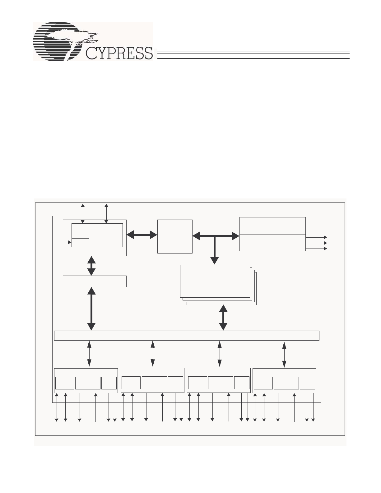
Figure 1-1. Blo ck Diagram
CY7C65640
TetraHub™ High-Speed USB Hub Controll
1.0 TetraHub™ Features
• USB 2.0 hub
• Four downstream port s
• Multiple transact ion translators— one per downstream
port for maximum performance
• VID, PID, and DID configured from external SPI
EEPROM
• 24-MHz external crystal
• Small package—Quad Flat Pack, no leads (QFN)
• Integrated up stream pull-up resist or
• Integrated downstream pull-down resistors for all
downstream ports
• Integrated up stream and downstream series termination resistors
.
D+ D–
Serial
Interface
Engine
24 MHz
Crystal
USB 2.0 PHY
PLL
USB Upstream Port
• Configurable with external SPI EEPROM
—N umb er of Active Ports
—N umb er of Removabl e Ports
—Maximum Power
—Hub Controller Power
—Power-On Timer
—Overcurrent Timer
—Disable Overcurrent Timer
—Enable Full-speed Only
—Disable P o rt Indicators
—Gang Power switching
—Enable Single TT Mode Only
—Enable NoEOPatEOF1
High-Speed
USB Control Logic
SPI Communication
Block
SPI_SCK
SPI_SD
SPI_CS
Hub Repeater
USB Downstream Port 1
PHY
D–
Port Power
Control
OVR#[1] LEDPWR#[1]
USB 2.0
D+
Port
Status
USB Downstream Port 2
PHY
D–
Port Power
Control
USB 2.0
D+
OVR#[2] LEDPWR#[2]
Routing Logic
Port
Status
USB 2.0
D+
Transaction Translator (X4)
TT RAM
USB Downstream Port 3
PHY
D–
Port Power
Control
Port
Status
OVR#[3] LEDPWR#[3]
USB Downstream Port 4
PHY
D–
Port Pow e r
Control
OVR#[4] LEDPWR#[4]
USB 2.0
D+
Port
Status
Cypress Semiconductor Corporation • 3901 North First Street • San Jose, CA 95134 • 408-943-2600
Document #: 38-08019 Rev. *H Revised August 2, 2005
Page 2

A
CY7C65640
2.0 Introduction
Cypress’s TetraHub is a high-performance self-powered
Universal Serial Bus (USB) 2.0 hub. The Tetra architecture
provides four downstream USB ports, with a Transaction
Translator (TT) for each port, making it the highest-performance hub possi ble. T his si ngle-c hip devi ce inco rporat es on e
upstream and four downstream USB transceivers, a Serial
Interface Engine (SIE), USB Hub Controller and Repeater , and
four TTs. It is suitable for standalone hubs, mot her board hu bs,
and monitor hub applications.
Being a fixed-function USB device, there is no risk or added
engineering effort required for firmware development. The
developer does not need to wri te any firmwar e for their d esign.
The CY4602 Tetrahub USB 2.0 4-port Hub Reference Design
Kit provides all materials and documents needed to move
rapidly into production. The reference design kit includes
board schematics, bill of materials, Gerber files, Orcad files,
key applicat ion notes, and product description.
CY7C65640A-LFXC is a functional and pin equivalent die
revision of Cypress's CY7C65640-LFXC. Changes were
made to improve device performance.
2.1 TetraHub Architecture
Figure 1-1 is a block diagram of the TetraHub Architecture.
2.2 USB Serial Interface Engine (SIE)
The SIE allows the CY7C65640A to communicate with the
USB host through the USB repeater component of the hub.
The SIE handles the fol lowing USB bus activ ity indepen dent ly
of the Hub Control Block:
• Bit stuffing/unstuffing
• Checksum generation/checking
• ACK/NAK/STALL
• TOKEN type identification
• Address checking.
2.3 Hub Controller
The Hub Control Block do es t he followi ng pr otocol handli ng at
a higher level:
• Coordinate enumeration by respondi ng to SETUP packets
• Fill and empty the FIFOs
• Suspend/Resume coordination
• Verify and select DATA toggle values
• Port power contr ol and over-current det ection.
The Hub Controller provides status and control and permits
host access to the hub.
2.4 Hub Repeater
The Hub Repeater manages the connectivity between
upstream and downstream facing ports that are operating at
the same speed. It supports full-/low-speed connectivity and
high-speed connectivity. Per the USB 2.0 specification, the
Hub Repeater provides the following functions:
• Sets up and tear s d own connect ivi ty on pack et boundari es
• Ensures orderly entry into and out of the Suspend state,
including proper handling of remote wakeups.
2.5 Transaction Translator
The TT basically trans lates data fr om one speed to another. A
TT takes high-speed split transactions and translates them to
full-/low-speed transactions when the hub is op erating at high
speed (the upstream port is connected to a high-speed host
controller) and has full-/low-speed devices attached. The
operating speed of a device attac hed on a downst ream faci ng
port determines whether the Routing Logic connects a port to
the Transaction Translator or Hub Repeater section. If a low/full-speed device is connected to the hub operating at high
speed, the data transfer route includes the transaction translator. If a high-speed device is connected to this high-speed
hub the route only includes the repeater and no transaction
translator since the device and the hub are in conformation
with respect to their data transfer speed. When the hub is
operating at full speed (the upstream port is connected to a
full-speed host controller), a high-speed peripheral will not
operate at its ful l ca pab ili ty. These devic es wil l o nly wor k at 1. 1
speed. Full- and low-speed devices connected to t his hub will
operate at their 1.1 speed.
3.0 Applications
• Standalone Hubs
• Motherboard Hubs
• Monitor Hub applications
• External Per sonal Stor age Dri ves
• Port Replicators
• Portable Drive
• Docking Stations
4.0 Functional Overview
The Cypress TetraHub USB 2.0 Hub is a high-performance,
low-system-cost solution fo r USB. Th e TetraHub USB 2.0 Hub
integrates 1.5k upstream pull-up resistors for full-speed
operation and all downstream 15k pull-down resistors as well
as series termination resistors on all upstream and
downstream D+ and D– pins. This results in optimization of
system costs by providing built-in support for the USB 2.0
specification.
4.1 System Initialization
On power-up, t he TetraHub will read an ex ternal SPI EE PROM
for configuration information. At the most basic level, this
EEPROM will have the Vendor ID (VID), Product ID (PID), and
Device ID (DID) for the customer's application. For more
specialized applications, other configuration options can be
specified. See section 8.0 for more detai ls.
After reading the EEPROM, if BUSPOWER (connected to upstream VBus) is HIGH, TetraHub will enable the pull-up
resistor on the D+ to indicate that it is connected to the
upstream hub, after which a USB Bus Reset is expected.
During this reset, TetraHub will initiate a chirp to indicate that
it is a high-speed peripheral. In a USB 2.0 system, the
upstream hub will respond with a chirp sequence, and
TetraHub will be in a high- speed mode, with the upstre am D+
Document #: 38-08019 Rev. *H Page 2 of 21
Page 3

A
CY7C65640
pull-up resistor turned off. In USB 1.x systems, no such chirp
sequence from the upstream hub will be seen, and TetraHub
will operate as a normal 1.x hub (operating at full speed).
4.2 Enumeration
After a USB Bus Reset, TetraHub is in an unaddressed, un configured stat e (configur ation value set to 0). During the enu meration process, the host will set the hub's address and configuration by sending a SetCongfiguration request. Changing the
hub address will restore it to an unconfigured state.
For high-speed multi-TT support, the host must also set the
alternate interface setti ng to 1 (the def ault mode i s singl e-TT).
Once the hub is configured, the full hub functionality is
available.
4.3 Multiple Transaction Translator Support
After TetraHub is configured in a high-speed system, it will be
in Single TT mode. The host may th en set the hub i nto Multipl e
TT mode by sending a SetInterface command. In Multiple TT
mode, each full -speed por t is han dled ind epende ntly an d thus
has a full 12-Mbp s ban dwidt h av ailab le. In Si ngle T T mode, all
traffic f rom the host desti ned for full - or low- spee d port s wil l be
forwarded to all of those ports. This means that the 12-Mbps
bandwidth is shared by all full- and low-speed ports.
4.4 Downstream Ports
T etraHub supp orts a maximum of four downstream port s, each
of which may be marked as usable or removable in the
extended configuration (0xD2 EEPROM load, see section
8.2). Downstream D+ and D– pull-down resistors are incorporated in TetraHub for each port. Prior to the hub being
configured, the ports are driven SE0 (Single Ended Zero,
where both D+ and D– are driven LOW) and are set to the
unpowered sta te. Once the hub is c onfigured, t he ports are not
driven, and the host may power the ports by sending a
SetPortPower command to each port. After a port is powered,
any connect or disconnect event is detected by the hub. Any
change in the port sta te is report ed by the hub back to the host
through the Status Change Endpoint (endpoint 1). Upon
receipt of SetPort R eset command from the host, the hub will
• Drive SE0 on the corresponding port
• Put the port in an enabled state
• Enable the green por t indicator for that port (i f not previously
overridden by t he host)
• Enable babble detection once the port is enabl ed.
Babble consists of either unterminated traffic from a
downstream port (o r loss of activi ty), or a non-idle condi tion on
the port after EOF2. If babble is detected on an enabled port,
that port will be disabl ed. A Cle arPort Enable comm and from
the host will also disable the specifie d port.
Downstream ports can be individually suspended by the host
with the SetPortSuspend command. If the hub is not
suspended, any res ume will be con fined t o that in divid ual port
and reflected to the host through a port change indication in
the Hub Status Change Endpoint. If the hub is suspended, a
resume on this port will be forwarded to the host, but other
resume events will not be seen on that port. The host may
resume the port by sendi ng a ClearPortSuspend com m and.
4.5 Upstream Port
The upstream port includes the transmitter and the receiver
state machine. The Transmitter and Receiver operate in highspeed and full-speed depending on the current hub configuration.
The transmitter state machine monitors the upstream facing
port while the Hub Repeater has connectivity in the upstream
direction. This monitoring activity prevents propagation of
erroneous indications in the upstream direction. In particular,
this machine prevents babble and disconnect events on the
downstream facing ports of this hub from propagating and
causing the hub to be disabled or disconnected by the hub to
which it is attached. This allows the Hub t o only disconnect t he
offensive port on detecting a babble from it.
4.6 Power Switching
TetraHub includes interface signals for external port power
switches. Both ganged and individ ual (per-p ort) configu rations
are supported, with individual switching being the default.
Initially all ports are unpowered. After enumerating, the host
may power each port by sending a SetPortPower command
for that port. The power switching and over-current detection
of downstream ports is m anaged by control pins connected to
an external power switch device. PWR [n]# output pins of the
CY7C65640A series ar e connected to t he respective e xternal
power switch's port power enable sign als. (Note that each port
power output pin of the external power switch must be
bypassed with a n electro lytic or t anta lum capaci tor as requ ired
by the USB specification. These capacitors supply the inrush
currents, which occur during downstream device hot-attach
events.)
4.7 Over-current Detection
Over-current detection includes timed detection of 8 ms by
default. This parameter is configured from the external
EEPROM in a range of 0 ms to 15 m s for both an enabled por t
and a disabled port individually. Detection of over-current on
downstream ports is managed by control pins conn ected to an
external power switch device.
The OVR[n]# pins of the CY7C65640A series are connected
to the respective external power switch's port over-current
indication (output) signals. Upon detecting an over-current
condition, the hub device r eports the over-current condition to
the host and disables the PWR# output to the external power
device.
4.8 Port I ndicators
The USB 2.0 port indicators are also supported directly by
TetraHub. As per the specification, each downstream port of
the hub supports an option al st atus indic ator . The pre sence of
indicators for downstream facing ports is specified by bit 7 of
the wHubCharacter istics field of the hub class d escriptor. The
default TeraHub descriptor specifies that port indicators are
supported (wHubChar acteri sti cs, bit 7 is set). If po rt indi cator s
are not included in the hub, this should be disabled by the
EEPROM.
Each port indicator is strategically located directly on the
opposite edge of the port which it is associated with. The
indicator provides two colors: green an d am ber. This is i m plemented as two separate LEDs, one amber and the other
green. A combi nation of hardware and soft ware contr ol is u sed
Document #: 38-08019 Rev. *H Page 3 of 21
Page 4

A
CY7C65640
to infor m the us er of th e cu rrent sta tus of t he port o r the devic e
attached to the port and to guide the user through problem
resoluti on. Col ors a nd b linking ar e used to pr ovide info rmatio n
to the user. The significance of the color of the LED depends
on the operational mode of the TetraHub. There are two
modes of operat ion f or t he TetraHub port i ndicat ors: automat ic
and manual.
On power-up the TeraHub defaults t o Automatic Mode, where
the color of the Port Indicato r (Green, Amber , Off) indicates the
functional status of the TetraHub port. In Automatic Mode,
TetraHub will turn on the green LED whenever the port is
enabled and the amber LED when it has had an over-current
condition detected. Th e color of the port indicator is set by th e
port state machine. Blinking of the LEDs is not supported in
T able 4-1. Automatic Port State to Port Indicat or Color Mapping
Downstream Facing Hub Port State
Port
Switching
With Off or Amber if due to an
Overcurrent Condition
Without Off Off or Amber if due to an
Table 4-2. Port Indicator Color Definitions in Manual Mode
Color Definition Port State
Off Not operational
Amber Error condition
Green Fully Operational
Blinking Off/Green Software Attention
Blinking Off/Amber Hardware Attention
Blinking Green/Amber Reserved
Powered Off
Disconnected, Disabled, Not
Configured, Reset ti ng, Testing
Off Green Off
Overcurrent Conditi on
Automatic Mode. Table 4- 1 below identifies the mapping of
color to port state in Automatic Mode.
In manual mode, the indicators are under the control of the
host, which can turn on one of the LEDs, or leave them off.
This is done by a system software USB Hub class request.
Blinking of the LEDs is supported in Manual Mode. The port
indicators allow the user to intervene on any error detection.
For example, when babble is detected on plugging in a
defective de vice, or on occurr ence of an o vercurren t condit ion,
the port indicators corresponding to the downstream port will
blink green or only light the amber LED, respectively. Table 4-
2 below displays the color definition of the indicators when
TetraHub is in Manual Mode.
Enabled, T r ansmit,
or Tr ansm itR
Green Off
Suspended, Resuming,
SendEOR, Restart_E /S
Note. Informati on present ed in Table 4-1 and Table 4-2 is from
USB 2.0 specificati on Tables 11- 6 and 11-7, respectively.
Document #: 38-08019 Rev. *H Page 4 of 21
Page 5

A
5.0 Pin Configuration
CY7C65640
DD–[4]
DD+[4]
VCC
GND
DD–[3]
DD+[3]
VCC
GND
DD–[2]
DD+[2]
VCC
GND
PWR#[3]
VCC
545556
OVR#[3]
53 52
PWR#[4]
GND
OVR#[4]
51 50 49 48 47 46 45 44 43
SPI_SD
GND
SPI_SCK
RESET
1
2
3
4
5
6
7
8
9
10
11
AMBER#[4]
VCC
GREEN#[4]
AMBER#[3]
42
41
GREEN#[3]
40
GND
VCC
39
38
AMBER#[2]
GREEN#[2]
37
AMBER#[1]
36
GREEN#[1]
35
GND
34
33
VCC
32
OVR#[2]
GND
DD–[1]
DD+[1]
12
13
14
2827262524232221201918171615
D–
D+
GND
VCC
VCC
XIN
GND
VCC
XOUT
GND
SPI_CS
BUSPOWER
VCC
GND
31
30
29
PWR#[2]
OVR#[1]
PWR#[1]
Figure 5-1. 56-pin Quad Flat Pack No Leads (8 mm x 8 mm)
Document #: 38-08019 Rev. *H Page 5 of 21
Page 6

A
CY7C65640
6.0 Pin Description Table
Table 6-1 below displays the pin assignments for the
CY7C65640A.
T able 6-1. Pin Assignments
Pin Name Type Default Description
3 VCC Power N/A V
7 VCC Power N/A V
11 VCC Power N/A V
15 VCC Power N/A V
19 VCC Power N/A V
23 VCC Power N/A V
27 VCC Power N/A V
33 VCC Power N/A V
39 VCC Power N/A V
45 VCC Power N/A V
55 VCC Power N/A V
4 GND Power N/A GND. Connect to Ground with as short a path as possible.
8 GND Power N/A GND. Connect to Ground with as short a path as possible.
12 GND Power N/A GND. Connect to Ground with as short a path as possible.
16 GND Power N/A GND. Connect to Ground with as short a path as possible.
20 GND Power N/A GND. Connect to Ground with as short a path as possible.
24 GND Power N/A GND. Connect to Ground with as short a path as possible.
28 GND Power N/A GND. Connect to Ground with as short a path as possible.
34 GND Power N/A GND. Connect to Ground with as short a path as possible.
40 GND Power N/A GND. Connect to Ground with as short a path as possible.
47 GND Power N/A GND. Connect to Ground with as short a path as possible.
50 GND Power N/A GND. Connect to Ground with as short a path as possible.
56 GND Power N/A GND. Connect to Ground with as short a path as possible.
21 XIN Input N/A 24-MHz Crystal IN or External Clock Input.
22 XOUT Output N/A 24-MHz Crystal OUT.
46 RESET# Input N/A Active LOW Reset. This pin resets the entire chip. It is normally tied to V
26 BUSPOWER Input N/A VBUS. Connect t o the VBUS pin of the up stream connecto r. Th is signal indicates
SPI INTERFACE
25 SPI_CS O O SPI Chip Select. Connect to CS pin of the EEPROM.
48 SPI_SCK O O SPI Clock. Connect to EEPROM SCK pin.
49 SPI_SD I/O/Z Z SPI Dataline Connect to GND with 15-KΩ
UPSTREAM PORT
17 D– I/O/Z Z Upstream D– Signal.
18 D+ I/O/Z Z Upstream D+ Signal.
DOWNSTREAM PORT 1
13 DD–[1] I/O/Z Z Downstream D– Signal.
. This signal provid es power to the chip.
CC
. This signal provid es power to the chip.
CC
. This signal provid es power to the chip.
CC
. This signal provid es power to the chip.
CC
. This signal provid es power to the chip.
CC
. This signal provid es power to the chip.
CC
. This signal provid es power to the chip.
CC
. This signal provid es power to the chip.
CC
. This signal provid es power to the chip.
CC
. This signal provid es power to the chip.
CC
. This signal provid es power to the chip.
CC
through a 100K resisto r , and t o GND through a 0.1-µF cap acitor. Other than this,
no other special power- up procedure is requir ed.
to the hub that it is in a powered st ate, and may enable the D+ pull-up resistor
to indicate a connec tion. (The hub wi ll do so af ter the exter nal EEPROM is read,
unless it is put i nto a high-speed mode by the upstream hub). The hub can not
be bus powered, and the VBUS signal must not be used as a power source.
resistor and to the Data I/O pins of
the EEPROM.
CC
Document #: 38-08019 Rev. *H Page 6 of 21
Page 7

A
T able 6-1. Pin Assignments (continued)
Pin Name Type Default Description
14 DD+[1] I/O/Z Z Downstream D+ Signal.
36 AMBER#[1] O 1 LED. Driver output for Amber LED. Port Indicator Support. Activ e LOW.
35 GREEN#[1] O 1 LED. Driver output for Green LED. Port Indicator Support. Active LOW.
30 OVR#[1] Input 1 Overcurrent Condition Detection Input. Active LOW.
29 PWR#[1] O/Z Z Power Switch Driver Output . Active LOW.
DOWNSTREAM PORT 2
9 DD–[2] I/O/Z Z Downstream D– Signal.
10 DD+[2] I/O/Z Z Downstream D+ Signal.
38 AMBER#[2] O 1 LED. Driver output for Amber LED. Port Indicator Support. Activ e LOW.
37 GREEN#[2] O 1 LED. Driver output for Green LED. Port Indicator Support. Active LOW.
32 OVR#[2] Input 1 Overcurrent Condition Detection Input. Active LOW.
31 PWR#[2] O/Z Z Power Switch Driver Output . Active LOW.
DOWNSTREAM PORT 3
5 DD–[3] I/O/Z Z Downstream D– Signal.
6 DD+[3] I/O/Z Z Downstream D+ Signal.
42 AMBER#[3] O 1 LED. Driver output for Amber LED. Port Indicator Support. Activ e LOW.
41 GREEN#[3] O 1 LED. Driver output for Green LED. Port Indicator Support. Active LOW.
53 OVR#[3] Input 1 Overcurrent Condition Detection Input. Active LOW.
54 PWR#[3] O/Z Z Power Switch Driver Output . Active LOW.
DOWNSTREAM PORT 4
1 DD–[3] I/O/Z Z Downstream D– Signal.
2 DD+[3] I/O/Z Z Downstream D+ Signal.
44 AMBER#[3] O 1 LED. Driver output for Amber LED. Port Indicator Support. Activ e LOW.
43 GREEN#[3] O 1 LED. Driver output for Green LED. Port Indicator Support. Active LOW.
51 OVR#[3] Input 1 Overcurrent Condition Detection Input. Active LOW.
52 PWR#[3] O/Z Z Power Switch Driver Output . Active LOW.
CY7C65640
Unused port DD+/DD– lin es can be lef t floati ng. The po rt power, amber , and gr een LED pins should be l eft unco nnected, and the
overcurrent pin should be tied HIGH. The overc urrent pin is an input and it shou ld not be left floati ng.
7.0 Default Descriptors
7.1 Device Descriptor
The standard device descri ptor for TetraHub is based on the VID, PID, and DI D found in the SPI EEPROM. This VID/PID/DID in
the EEPROM will overwrite the default VID/PID/DID. If no EEPROM is used, the TetraHub will enumerate with the default
descriptor values as shown below.
Byte Full Speed High Speed Field Name Description
0 0x12 0x12 bLength 18 Bytes
1 0x01 0x01 bDescriptorType DEVICE_DESCRIPTOR
2,3 0 x0200 0x0200 bcdUSB USB specification 2.0
4 0x09 0x09 bDeviceClass HUB
5 0x00 0x00 bDeviceSubClass None
6 0x00 0x02 bDeviceProtocol None
7 0x40 0x40 bMaxPacketSize0 64 bytes
8,9 0x04B4 0xx04B4 wIdVendor VID (overwritten by what is defined in EEPROM)
10,11 0x6560 0x6560 wIdProduct PID (overwritten by what is defined in EEPROM)
Document #: 38-08019 Rev. *H Page 7 of 21
Page 8

A
Byte Full Speed High Speed Field Name Description
12, 13 0x000B 0x000B wbcdDevice DID (overwritten by what is defined in EEPROM)
14 0x00 0x00 iManufact urer No manufacturer string sup ported
15 0x00 0x00 iProduct No product stri ng supported
16 0x00 0x00 iSerialNumber No serial string supported
17 0x01 0x01 bNumConfigur ations One configuration supported
CY7C65640
7.2 Configuration Descriptor
Byte Full Speed High Speed Field Name Description
0 0x09 0x09 bLength 9 Bytes
1 0x02 0x02 bDescriptorType CONFIG_DESCRIPTOR
2 0x0019 0x0029
4 0x01 0x01 bNumInterfaces 1
5 0x01 0x01 bConfigurationValue The configuration to be used
6 0x00 0x00 iConfiguration
70xE0 0xE0bmAttributes
80x32 0x32
[1]
[2]
wTota lLength Length of all other des criptors
bMaxPower
7.3 Interface Descriptor
Byte Full Speed High Speed Field Name Description
0 0x09 0x09 bLength 9 Bytes
1 0x04 0x04 bDescriptorType INTERFACE_DESCRIPTOR
2 0x00 0x00 bInterfaceNumber
3 0x00 0x00 bAlternateSetting
4 0x01 0x01 bNumEndpoints
5 0x09 0x09 bInterfaceClass
6 0x00 0x00 bInterfaceSubClass
7 0x00 0x01 bInterfaceProtocol
80x00 0x00iInterface
7.4 Endpoint Descriptor
Byte Full Speed High Speed Field Name Description
0 0x07 0x07 bLength 7 Bytes
1 0x0 5 0x05 bDescriptorType ENDPOINT_DESCRIPTOR
2 0x81 0x81 bEndpointAddress IN Endpoint #1
3 0x03 0x03 bmAttributes Interrupt
4,5 0x0001 0x0001 wMaxPacketSize Maximum Packet Size
6 0xFF 0x0C bInterval Polling Rate
Notes:
1. This value is reported as 0x19 if the hub is configured in Single-TT mode.
2. This value is configured through the External EEPROM.
Document #: 38-08019 Rev. *H Page 8 of 21
Page 9

A
CY7C65640
7.5 Interface Descriptor
I
[3]
Byte Full Speed High Speed Field Name Description
0 N/A 0x09 bLength 9 Bytes
1 N/A 0x04 bDescriptorType INTERFACE_DESCRIPTOR
2 N/A 0x00 bInterfaceNumber Interface Desc ri ptor Index
3 N/A 0x01 bAlternateSetting Alternate Setting for th e Interface
4 N/A 0x01 bNumEndpoints Number of Endpoints Defined
5 N/A 0x09 bInterfaceClass Interface Class
6 N/A 0x00 bInterfaceSubClass Interface Sub-Class
7 N/A 0x02 bInterfaceProtocol Interface Protocol
8 N/A 0x00 bInterface Interface String Index
7.6 Endpoint Descriptor
[3]
Byte Full Speed High Speed Field Name Description
0 N/A 0x07 bLength 7 Bytes
1 N/A 0x05 bDescriptorType ENDPOINT_DESCRIPTOR
2 N/A 0x81 bEndpointAddress IN Endpoint #1
3 N/A 0x03 bmAttributes Interrupt
4,5 N/A 0x0001 w MaxPacketSize Maximum Packet Siz e
6 N/A 0x0C bInterval Polling Rate
7.7 Device Qualifier Descriptor
Byte Full Speed High Speed Field Name Description
0 0x0A 0x0A bLength 10 Bytes
1 0x06 0x06 bDescriptorType DEVICE_QUALIFIER
2,3 0x0200 0x0200 bcdUSB
4 0x09 0x09 bDeviceClass
5 0x00 0x00 bDeviceSubClass
6 0x02 0x00 bDeviceProtocol
7 0x40 0x40 bMaxPacketSize0
8 0x01 0x01 bNumConfigurations
9 0x00 0x00 bReserved
Note:
3. If TetraHub is configured for single-TT only (from the external EEPROM), this descriptor is not present.
Document #: 38-08019 Rev. *H Page 9 of 21
Page 10

A
7.8 Hub Descriptor
Byte All Speeds Field Name Description
0 0x09 bLength 9 Bytes
1 0x29 bDescriptorType HUB Descr iptor
[4]
20x04
3,4 0x0089
50x32
60x64
70x00
80xFF
bNbrPorts Number of ports supported
[4]
wHubCharacteristi cs b1, b0: Logical Power Switching Mode
00: Ganged power switch ing (all ports’ power at once)
01: Individual port power switching (Default in TetraHub)
b2: Identifies a Compou nd Device,
0: Hub is not part of a compound device (Default in TetraHub),
1: Hub is part of a compou nd device.
b4, b3: Over-current Protection Mode
00: Global Overcur rent Protection. The hub reports overcurr ent as a
summation o f all port s curr ent draw , without a br eakdown of individu al port
overcurrent status.
01: Individual Port Overcurr ent Protection. The h ub reports ov ercurrent on
a per-port basis. Each port has an over-curr ent status (Default in
TetraHub).
1X: No Overcurrent Protection. This option is allowed only for buspowered hubs that do not implement overcurrent protection.
b6, b5: TT Think Tim e
00: TT requires at most 8 FS bit times of inter transac tion gap on a
full-/low-speed downstream bus (Default in TetraHub).
01: TT requires at most 16 FS bit ti me s.
10: TT requires at most 24 FS bit ti me s.
11: TT requires at most 32 FS bit times.
b7: Port Indicator s Supported,
0: Port Indicators are not supported on its downstream facing ports and
the PORT_INDICATOR request has no effect .
1: Port Indicators are supported on its downstream facing ports and the
PORT_INDICAT O R request controls the indicat ors. See Section 4 and 9
(Default in TetraHub).
b15...b8: Reserved
[4]
bPwrOn2PwrGood Time from when the port is power ed to when the power is good on that port
[4]
bHubContrCurrent Maximum current requirement for the Hub Controller
[4]
bDeviceRemovable Indicates if the port has a removable device attached
[4]
bPortPwrCtrlMask Required for compatibility with soft w are written for 1.0 compliant devices
CY7C65640
Note:
4. This value is configured through the External EEPROM.
Document #: 38-08019 Rev. *H Page 10 of 21
Page 11

A
CY7C65640
8.0 Configuration Options
Systems using TetraHub must have an external EEPROM in
order for the device to have a unique VID, PID, and DID. The
TetraHub can talk to SPI EEPROM that are double byte
addressable only. Tet raHub uses the command format from
the '040 parts. The TetraHub cannot talk to ‘080 EEPROM
parts, as the read command format used for talking to ‘080 is
not the same as ‘040. The '010s and '020s uses the same
command format as used t o inter face with th e ‘040 and henc e
these can also be used to interface with the TetraHub.
8.1 Default – 0xD0 Load
When used in default mod e, onl y a unique VID, PID, and DID
must be present in the external SPI EEPROM. The contents
of the EEPROM must contain this information in the following
format:
Byte Value
00xD0
1 VID (LSB)
2 VID (MSB)
3 PID (LSB)
4 PID (MSB)
5 DID (LSB)
6 DID (MSB)
8.2 Configured – 0xD2 Load
Byte Value (MSB->LSB)
00xD2
1VID (LSB)
2 VID (MSB)
3PID (LSB)
4 PID (MSB)
5 DID (LSB)
6 DID (MSB)
7 EnableOverCurrentTimer[3:0] , Di sableOvercurr ent-
Timer[3:0]
8 ActivePo rts[3:0], Rem o v ableP o rts[3:0]
9MaxPower
10 HubControllerPower
11 PowerOnTimer
12 IllegalHubDescriptor, Unused, FullspeedOnly ,
NoPortIndicators , Reserved, Gan gPowered, SingleT-
TOnly, NoEOPatEOF1
Byte 0: 0xD2
Needs to be programmed with 0x D2
Byte 1: VID (LSB)
Least Significant Byte of Vendor ID
Byte 2: VID (MSB)
Most Significant Byte of Vendor ID
Byte 3: PID (LSB)
Least Significant Byte of Product ID
Byte 4: PID (MSB)]
Most Significant Byte of Product ID
Byte 5: DID (LSB)
Least Significant Byte of Device ID
Byte 6: DID (MSB)]
Most Significant Byte of Device ID
Byte 7: EnableOvercurrentTimer[3:0], DisabledOvercurrentTimer[3:0]
Count time in ms fo r filtering o vercurrent detection. Bits 7–4
are for an enabled port, and bits 3–0 are for a disabled por t.
Both range from 0 ms t o 15 ms. See section 4 .8. Default: 8
ms = 0x88.
Byte 8 : ActivePo rts [3 :0 ], Remo va b le P o r ts[3 : 0 ]
Bits 7–4 are the ActivePorts[3:0] bits that indicates if the
corresponding port is usable. For example, a two-port hub
that uses port s 1 and 4 wou ld set th is field t o 0x09. The t otal
number of ports reported in the Hub Descriptor: bNbrPorts
field is calculated from this. Bits 3–0 are the RemovablePorts[3:0] bits that indicates whether the corresponding
port is removable (set to HIGH). This bit’s values are recorded appropriately in the
HubDescriptor:DeviceRemovable fiel d. Default: 0xFF.
Byte 9: MaximumPower
This value i s reported in the Confi gurationDes criptor:bMax Power field and is the current in 2-mA intervals that is required from the upstream hub. Default: 0x32 = 100 mA
Byte 10: HubControllerPower
This value is re ported in t he HubDescri ptor:bHub Contr Current field and is th e curr ent in milliamper es required by the
hub controller. Default: 0x64 = 100 mA.
Byte 11: PowerOnTimer
This value is reported in the HubDescriptor:bPwrOn2PwrGood f ield and is t he time in 2-ms interval s
from the SetPortPower command until the power on the
corresponding downstream port is good. Default: 0x32 =
100 ms.
Byte 12: IllegalHubDescriptor, Unused, FullspeedOnly,
NoPortIndicators, Reserved, GangPowered, SingleTTOnly, NoEOPatEOF1
Bit 7: Illeg alHubDescriptor: For GetHubDesc ri ptor request,
some USB hosts use a DescriptorTypeof 0x00 instead of
HUB_DESCRIPTOR, 0x29. According to the USB 2.0 st andard, a hub must treat thi s as a Request Error, and STALL
the transaction accordingly (USB 2.0, 11.24.2.5). For systems that do not accept this, the IllegalHubDescriptor configuration bit may be set to allow TetraHub to accept a DescriptorType of 0x00 for this command. Default is 0,
recommended setting is 1.
Bit 6: Unused: This bit is an unused, don’t care bit and can
be set to anything.
Bit 5: Fullspeed: Only configures t he hub to be a full -speed
only device. Default set to 0.
Document #: 38-08019 Rev. *H Page 1 1 of 21
Page 12

A
CY7C65640
Bit 4: NoPortIndicators: Turns off the port indicators and
does not report them as present in the HubDescriptor,
wHubCharacteristics b7 field. Default set to 0.
Bit 3: Reserved: This bit is reserved and should not be set
to 1. Must be set to 0.
Bit 2: GangPowered: Indicates whether the port power
switching is ganged (set to 1) or per-port (set to 0). This is
reported in the HubDescriptor, wHubCharacteristics field,
b4, b3, b1, and b0. Default set to 0.
Bit 1: SingleTT Only: Indi cates that the hub shoul d only support single T ransact ion Tran slator mode. This changes var ious descriptor values. Default set to 0.
Bit 0: NoEOPatEOF1 tur ns of f the EOP gener ation at EOF1
in full-spee d mode. Note that s everal USB 1.1 h osts can not
handle EOPatEOF1 properly. Cypress recommends that
this option be turned off for general-purpose hubs. Default
is 0, recommended setting is 1.
9.0 Supported USB Requests
9.1 Device Class Commands
Table 9-1. Device Class Requests
Request bmRequestType bRequest wValue wIndex wLength Data
GetDev iceStatus 10000000B 0x00 0x0000 0x0000 0x0002 2 Byte Devi ce Status
GetInterfaceStatus 10000001B 0x00 0x0000 0x0000 0x0002 2 Byte Endpoint
GetEndpointStatus 10000010B 0x00 0x0000 0x0000 0x0002 2 Byte Endpoint
GetDev iceDescriptor 10000000B 0x06 0x0001 Zero or
GetConfigDescriptor 10000000B 0x06 0x0002 Zero or
GetDeviceQualifierDescriptor
GetOtherSpeedConfigurationDescriptor
GetConfiguration
SetCongfiguration
GetInterface 100000 01B 0xA 0x0000 0x0000 0x0001 Interface Number
SetInterface 00000001B 0x0B Alternate
SetAdd ress 00000000B 0x05 Device Address 0x0000 0x0000 None
SetDeviceRemoteWakeup 00000000B 0x03 0x01 0x0000 0x0000 None
SetDeviceTest_J 00000000B 0x03 0x02 0x0100 0x0000 None
SetDeviceTest_K 00000000B 0x03 0x02 0x0200 0x0000 None
SetDeviceTest_SE0_NAK 00000000B 0x03 0x02 0x0300 0x0000 None
SetDeviceTest_Packet 00000000B 0x03 0x02 0x0400 0x0000 None
SetEndpointHalt 00000000B 0x03 0x00 0x0000 0x0000 None
ClearDeviceRe-
moteWakeup
ClearEndpointHalt 00000000B 0x01 0x00 0x0000 0x0000 None
Note:
5. Only one configuration is supported in TetraHub.
[5]
[5]
100000 00B 0x06 0x0006 Zero or
100000 00B 0x06 0x0007 Zero or
10000000B 0x08 0x0000 0x0000 0x0001 Configuration value
00000000B 0x09 Configuration
Value
Setting
00000000B 0x01 0x01 0x0000 0x0000 None
Language ID
Language ID
Language ID
Language ID
0x0000 0x0000 None
Interface
Number
Descriptor
Length
Descriptor
Length
Descriptor
Length
Descriptor
Length
0x0000 None
Status
Status
Descriptor
Descriptor
Descriptor
Descriptor
Document #: 38-08019 Rev. *H Page 12 of 21
Page 13

A
CY7C65640
9.2 Hub Class Commands
T able 9-2. Hub Class Requests
Request bmRequestType bRequest wValue wIndex wLength Data
GetHubS tatus 10100000B 0x00 0x0000 0x0000 0x000 4 Hub Status (See Table 11-19
of Spec) Ch ange St atus (See
Table 11-20 of Spec)
GetPortStatus 10100011B 0x00 0x0000 Byte 0: 0x00
Byte 1: Port
ClearHubFeatur e 00100000B 0x01 Feature Selectors
[6]
0x0000 0x0000 None
0 or 1
[6]
ClearPortFeature 00100011B 0x01 Feature Selectors
1, 2, 8, 16, 17 , 18, 19,
Byte 0: 0x00
Byte 1: Port
or 20
ClearPortFeature 00100011B 0x01 Feature
Selectors
(PORT_INDICATOR)
[6]
22
Byte 0:
Selectors
0, 1, 2, or 3
Byte 1: Port
SetHubFeature 00100000B 0x03 Feature
Selector
SetPortFeature 00100011B 0x03 Feature
Selectors
[6]
[6]
0x0000 0x0000 TetraHub STALLs this
Port 0x0000 None
2, 4 or 8
SetPortFeature 00100011B 0x03 Feature
Selector
(PORT_TEST)
[6]
21
Byte 0:
Selectors
1,2, 3, 4 or 5
Byte 1: Port
SetPortFeature 00100011B 0x03 Feature
Selector
(PORT_INDICATOR)
[6]
22
Byte 0:
Selectors
0, 1, 2, or 3
Byte 1: Port
GetHubDescriptor 10100000B 0x06 Descriptor Type and
Descriptor Index
ClearTTBuffer 00100011B 0x08 Dev_Addr, EP_Num TT_Port 0x000 0 None
ResetTT 00100000B 0x09 0x0000 Byte 0: 0x00
Byte 1: Port
GetTTS tate 10100011B 0X0A TT_Flags Byte 0: 0x00
Byte 1: Port
Stop TT 00100011B 0x0B 0x0000 Byte 0: 0x00
Byte 1: Port
Notes:
6. Feature selector values for different features are presented in Table 9-3.
7. Selector values for different features are presented in Table 9-5.
8. Selector values for different features are presented in Table 9-4.
0x0004 Port Status (See Table 11- 21
of Spec) Ch ange St atus (See
Table 11-20 of Spec)
0x0000 None
0x0000 None
[7]
request
0x0000 None
[8]
0x0000 None
[7]
Hub
Descriptor
Length
0x0000 None
TT State
TT State
Length
0x0000 None
Document #: 38-08019 Rev. *H Page 13 of 21
Page 14

A
CY7C65640
T able 9-3. Hub Class Feature Selector
Feature Selector Recipient Value
C_HUB_LOCAL_POWER Hub 0
C_HUB_OVER_CURRENT Hub 1
PORT_CONNECTION Port 0
PORT_ENABLE Port 1
PORT_SUSPEND Port 2
PORT_RESET Port 4
PORT_POWER Port 8
PORT_LOW_SPEED Port 9
C_PORT_CONNECTION Port 16
C_PORT_ENABLE Port 17
C_PORT_SUSPEND Port 18
C_PORT_OVER_CURRENT Port 19
C_PORT_RESET Port 20
PORT_TEST Port 21
PORT_INDICATOR Port 22
10.0 Upstream USB Connection
The following is a schemat ic of the USB upstream connector.
T able 9-4. Test Mode Selector for Feature Selector
PORT_TEST (0x21)
PORT_TEST Mode Description Selector Value
Test_J 1
Test_K 2
Test_SE0_NAK 3
Test_Packet 4
Test_Force_Enable 5
T able 9-5. Port Indicator Selector for Feature Selector
PORT_INDICATOR (0x22)
Port Indicator Color
Color Set Aut o matically as
shown in Table4-1
Selector
Value
Port Indicator
Mode
0 Automatic
Mode
Amber 1 Manual Mode
Green 2 Manual Mode
Off 3 Manual Mode
VCC
D–
D+
GND
SHELL
D–
D+
4.7 nF 250V
1 MΩ
Figure 10-1. USB Upstrea m Port Connect ion
11 .0 Downstream USB Connections
The following is a schematic of the USB downstream conn ector.
PWRx
150 µF
10V
0.01 µF
DD–[X]
DD+[X]
2.2 µF
10V
BUSPOWER
100 kΩ
VCC
D–
D+
GND
SHELL
Figure 11- 1. USB Downstream Port Connecti on
Document #: 38-08019 Rev. *H Page 14 of 21
Page 15

A
12.0 LED Connections
3.3V
The following is a schematic of the LED circuitr y.
GREEN#[x]
680Ω
CY7C65640
AMBER#[x]
Figure 12-1. USB Downstream Port Connection
680Ω
Document #: 38-08019 Rev. *H Page 15 of 21
Page 16

A
13.0 Sample Schemat i c
VCC
D–
D+
GND
SHELL
BUSPOWER
D–
D+
4.7 nF 250V
1 MΩ
2.2 µF
10V
100 kΩ
0.01 µF
680Ω
680Ω
CY7C65640
DD–[1]
DD+[1]
VCC
D–
D+
GND
SHELL
3.3V
5V
PWR1
OVR1
PWR2
OVR2
PWR3
OVR3
PWR4
OVR4
Power
Management
PWR4
PWR3
PWR2
PWR1
PWR1
150 µF
10V
GREEN#[1]
AMBER#[1]
BUSPOWER
3.3V
100K
0.1µF
D–
D+
DD–[1]
DD+[1]
DD–[2]
DD+[2]
DD–[3]
DD+[3]
DD–[4]
DD+[4]
3V
VCC1
VCC2
VCC3
VCC4
BUSPOWER
RESET
DD+
CY7C65640A-QFN
DD-[1]
DD+[1]
DD-[2]
DD+[2]
DD-[3]
DD+[3]
DD-[4]
DD+[4]
VCC5
VCC6
VCC7
VCC8
VCC9
SPI_SD
SPI_SCK
SPI_CS
SPI
EEPROM
SPI_SD
PWR2
150 µF
10V
0.01 µF
DD–[2]
DD+[2]
VCC
D–
D+
GND
SHELL
24 MHz
2 7pF
XIN
VCC10
VCC11
27 pF
XOUT
GREEN[1]
AMBER[1]
GREEN[2]
AMBER[2]
GREEN[3]
AMBER[3]
GREEN[4]
AMBER[4]
PWR1
PWR2
PWR3
PWR4
SPI_CS
SPI_SCK
SPI_SD
OVR1
OVR2
OVR3
OVR4
GREEN[1]
AMBER[1]
GREEN[2]
AMBER[2]
GREEN[3]
AMBER[3]
GREEN[4]
AMBER[4]
PWR1
OVR1
PWR2
OVR2
PWR3
OVR3
PWR4
OVR4
SPI_CS
SPI_SCK
SPI_SD
GREEN#[2]
AMBER#[2]
PWR3
150 µF
10V
GREEN#[3]
AMBER#[3]
PWR4
150 µF
10V
GREEN#[4]
680Ω
680Ω
680Ω
680Ω
680Ω
0.01 µF
0.01 µF
DD-[3]
DD+[3]
DD-[4]
DD+[4]
3.3V
VCC
D–
D+
GND
SHELL
3.3 V
VCC
D–
D+
GND
SHELL
3.3 V
GND1
GND2
GND3
GND4
GND5
GND6
GND7
GND8
GND9
GND10
GND11
GND12
AMBER#[4]
680Ω
Figure 13-1. Sample Schematic
Document #: 38-08019 Rev. *H Page 16 of 21
Page 17

A
CY7C65640
14.0 Electrical Characteristics
St ati c Discharge Voltage.. .......... .. .......... .. .......... .. .....> 2000V
Max. Ou tp u t S in k Cu rr e nt pe r I/ O........ ........................ 10 mA
14.1 Absolute Maximum Ratings
St orage Temperature ............... .. .......... .. ...–65°C to +150 °C
Ambient Temperature
with Pow er Ap p li ed ................. ..........................0°C to +7 0 °C
Supply Voltage to Ground Potential .............. –0.5V to +4.0V
DC Voltage Applied to Output s
in High Z State .......................................–0.5V to V
CC
+ 0.5V
Power Dissipation (4 HS ports)......................................1.6W
14.2 Oper ating Conditions
TA (Ambient Temperature Under Bias)............. 0°C to +70°C
Supply Voltage ................ .......... .. .......... .. ...+3.15V to +3.45V
Grou nd Voltage ............. ................................ .................... 0V
FOSC (Oscillator or Crystal Frequency).....24 MHz ± 0.05%,
parallel resonant, fundamental mode
14.3 DC Electrical Characteristics
Parameter Description Conditions Min. Typ. Max. Unit
V
CC
V
IH
V
IL
I
l
V
OH
V
OL
I
OH
I
OL
C
IN
I
SUSP
I
CC
USB Transceiver
Z
HSDRV
I
i
I
OZ
V
HSRS
T
rfi
Thermal Resistance
T
JA
Supp ly Voltage 3.15 3.3 3.45 V
Input High Voltage 2 5.25 V
Input Low Voltage –0.5 0.8 V
Input Leakage Current 0 < V
Output Voltage High I
Output Low Voltage I
< V
IN
CC
= 4 mA 2.4 V
OUT
= –4 mA 0.4 V
OUT
±10 µA
Output Current High 4mA
Output Current Low 4mA
Input Pin Capacitance 10 pF
Suspend Current 100 µA
Supply Current
4 Active port s Full-speed Host, Full-speed Devices 255 mA
High-speed Host, High-speed Devices 460 mA
High-speed Host, Full-speed Devices 395 mA
2 Active Ports Full-speed Host, Full-speed Devices 255 mA
High-speed Host, High-speed Devices 415 mA
High-speed Host, Full-speed Devices 380 mA
No Active Ports Full-speed Host 255 mA
High-speed Host 370 mA
Driver Output Resistance 41 45 49 Ω
Input Leakage Current ±0.1 ±5 µA
Three-stat e O utput OFF-State Current ±10 µA
High-speed Receiver Sensitivity Level 210 mV
Full-speed Fram e Jit ter 133 ns
Theta Thermal Coefficient Junction to
Ambient
E-Pad configura ti on in section 16.1
at zero airflow
23.27 °C/W
Document #: 38-08019 Rev. *H Page 17 of 21
Page 18

A
CY7C65640
14.4 AC Electrical Characteristics
Both the upstream USB transceiver and all four downstream
transceive rs have passed the USB-IF USB 2.0 Electrical Certificatio n Testing.
14.4.1 Serial Peripheral Interface
Parameter Description Conditions Min. Typ. Max. Unit
Clock Rise/Fall Time 500 ns
Clock Frequency 250 kHz
Data Set- up Time 50 ns
Hold Time 100 ns
Reset period 1.9 ms
14.4.2 Eye Diagram
15.0 Ordering Information
Ordering Code Package Type
CY7C65640A-LFXC 56-pin QFN Lead-free Package
CY4602 TetraHub USB 2.0 4 port Hub Refere nce Design Kit
Document #: 38-08019 Rev. *H Page 18 of 21
Page 19

A
16.0 Package Diagrams
The TetraHub is available in a space-saving 56-pin QFN
(8 × 8 mm)
.
56-Lead QFN 8 x 8 MM LF56A
CY7C65640
TOP VIEW
7.90[0.311]
8.10[0.319]
7.70[0.303]
7.80[0.307]
N
0.80[0.031]
A
1
2
DIA.
Dimensions are in millimeters
MIN
MAX
7.80[0.307]
7.70[0.303]
1.00[0.039] MAX.
0.80[0.031] MAX.
8.10[0.319]
7.90[0.311]
SIDE VIEW
0°-12°
Note. The bottom metal pad size varies by product due to die
size varia ble. I f met al pad desi gn or di mension a re c ritica l wit h
your board designs, please contact a Cypress Sales office to
get the specific out line option.
16.1 Quad Flat Package No Leads (QFN) Package Design Notes
The QFN (Quad Flatpack No Leads), being a lead free
package, t he electri cal c ont act o f the p art t o the Pr inted Circuit
Board (PCB) is made by soldering the lands on the bottom
surface of the package to t he PCB. Hence specia l at tention is
required to the heat transfer area bel ow the package to prov ide
a good thermal bond to the circuit board. A Copper (Cu) fill
should be designed into the PCB as a thermal pad under the
package. Heat is transferred from the TetraHub through the
device’s metal paddl e on the bottom side of the package. Heat
from here is conducted t o the PCB at the thermal pad. I t is the n
conducted from the thermal pad to the PCB inner ground plan e
by a 5 x 5 arra y of via. A via is a plated throug h-hole in the PCB
with a finis hed d iameter of 13 mil. The QFN’ s met al d ie paddl e
must be soldered to the PCB’s thermal pad. Solder mask is
placed on the board to p side over each via to res ist solder flow
BOTTOM VIEW
0.08[0.003]
C
0.05[0.002] MAX.
0.18[0.007]
E-PAD
(PAD SIZE VARY
BY DEVICE TYPE)
6.45[0.254]
6.55[0.258]
0.28[0.011]
0.50[0.020]
PIN1 ID
N
0.20[0.008] R.
1
2
0.45[0.018]
6.55[0.258]
6.45[0.254]
0.24[0.009]
(4X)
0.60[0.024]
51-85144-*D
0.20[0.008] REF.
0.30[0.012]
0.50[0.020]
C
SEATING
PLANE
into the via. The mask on the top side also minimizes
outgassing during the solder reflow process.
Please follow the layout guidel ines p rov ided i n the PCB l ayout
files accompanied with the CY4602 TetraHub Reference
Design Kit. The information in this section was derived from
the origin al applicat ion note by the p ackage vendor . For furthe r
information on this package design please refer to the application note “Surface Mount Assembly of AMKOR’s
MicroLeadFrame (MLF) Technology”. This application note
can be downloaded f rom AMKOR’s webs ite f rom the fo llowing
URL
http://www.amkor.com/products/notes_papers/MLF_AppNote
_0301.pdf.
This application note provides detailed information on board
mounting guidelines, soldering flow, rework process, etc.
Figure 16-1 below displ ays a cross- sec tiona l area underneat h
the package. The cross section is of only one via. The solder
Paste template needs to be designed to allow at least 50%
solder coverage. The thickness of the solder paste template
should be 5 mil. It is recommended that “No Clean”, type 3
solder paste is used for mounting the part. Nitrogen purge is
recommended during ref low.
Document #: 38-08019 Rev. *H Page 19 of 21
Page 20

A
Cu Fill
CY7C65640
0.017” dia
Solder Mask
Cu Fill
PCB Material
Via hole for thermally connecting the
QFN to the circuit board ground plane.
0.013” dia
This figure only shows the top three layers of the
circuit board: Top Solder, PCB Dielectric, and
the Ground Plane.
PCB Material
Figure 16-1. Cross-sect ion of the Area Underneat h the QFN Package
Figure 16-2a is a plot of the solder mask pattern and Figure 16-2b displays an X-Ray image of the ass embly (darker areas indicate
solder).
Figure 16-2a. Plot of the Solder Mas k (White Area)
Figure 16-2b. X-Ray Image of the Assembly
TetraHub is a trademark of Cypress Semiconductor Corporation. All product and company names mentioned in this document
may be the trademarks of their respective holders.
Document #: 38-08019 Rev. *H Page 20 of 21
© Cypress Semiconductor Corporation, 2005. The information contained herein is subject to change without notice. Cypress Semiconductor Corporation assumes no responsibility for the use
of any circuitry other than circuitry embodied in a Cypress product. Nor does it convey or imply any license under patent or other rights. Cypress products are not warranted nor intended to be
used for medical, life support, life saving, critical control or safety applications, unless pursuant to an express written agreement with Cypress. Furthermore, Cypress does not authorize its
products for use as critical components in life-support systems where a malfunction or failure may reasonably be expected to result in significant injury to the user. The inclusion of Cypress
Page 21

A
CY7C65640
Document History Page
Document Title: CY7C65640A TetraHub™ High-Speed USB Hub Controller
Document Number: 38-08019
REV. ECN NO. Issue Date
** 113506 04/25/02 BHA New Data Sheet (prelim inary)
*A 116812 08/15/02 MON Supply voltage range changed from 3.3V–3.6V to 3.15V–3.45
*B 118518 10/31/02 MON Fixed the Spec field in the Defau lt Device Descriptor section 7.1
*C 121793 12/09/02 MON Fixed the SPI clock Frequen cy to 250 KHz, section 14.4.1
*D 125275 04/02/03 MON Changed the name o f Bit 3 of Byte 12 of EEPROM f or a 0xD2 lo ad (section 8.2)
*E 234272 see ECN MON Added part number for the lead free package (CY7C65640-LFXC), section 15.0
*F 285171 see ECN KKU Changed CY7C65640 to CY7C65640A and reformatted to new format
*G 308296 see ECN KKU Added reset period under AC characteristics.
*H 390258 see ECN KKU added theta thermal coefficient junction to ambient (T
Orig. of
Change Descri ption of Change
Added EPROM types that can be used with HX2 (p. 14)
Added description of bit 7 of Byte 12 (Illegal Hub Descriptor) D2 Load (p. 15)
Added high speed sensit ivity level of receiver (p. 20)
Added QFN package desi gn notes (section 16.1)
Fixed Interface Protocol field of the i nterface descript or, section 7.3
Fixed Device Protocol field of the interface descriptor, section 7.7
Modified table 9-2, section 9.2
Added table 9-4, 9-5, section 9.2
Added table 4-1, 4-2, section 4.8
Added information on bits in wHubCharacterestics, section 7.8
Modified figure 16-1 in QFN package design n otes, section 16.1
Included the eye di agram, section 14.4.2
Preliminary to Final
Added information on the configuration of unused port pins, section 6.0
Added statement t hat no special power-up proc edure is required, sec ti on 6.0
from BusPowered to Reserved.
Removed all in dicat ion to the m isconc eption that the hub can suppo rt bus power.
Added information as to which ni bble of byt e 8 in the EEPROM defi nes the acti ve
ports and which nibble defines the removable ports, section 8.2.
Added further informati on on the BUSPOWER pin ( pin 26) functiona lity in section
6.0.
Changed the name of Bit 6 of Byte 12 of EEPROM for a 0xD2 load from
CompoundDevice to Unused, section 8.2.
Removed compound device from features list.
Update section 7.1 DID from 0x 0007 to 0x000B for rev E silicon.
) to section 14.3
JA
Document #: 38-08019 Rev. *H Page 21 of 21
 Loading...