


Page 1
CY7C64713/14
EZ-USB FX1™ USB Microcontroller
Full-speed USB Peripheral Controller
1.0 Features
• Single-chip integrated USB transceiver, SIE, and
enhanced 8051 microprocessor
• Fit, form and function upgradable to the FX2LP
(CY7C68013A)
—Pin-compatible
—Object-code-compatible
—Functionally-compatible (FX1 functionality is a
Subset of the FX2LP)
• Draws no more than 65 m A in any mode making the FX1
suitable for bus powered applications
• Software: 8051 runs from internal RAM, which is:
—Downloaded via USB
—Loaded from EEPROM
—External memory device (12 8-pin configuration only)
• 16 KBytes of on-chip Code/Data RAM
• Four programmable BULK/INTERRUPT/ISOCHRONOUS endpoint s
—Buffering options: double, triple, and quad
• Additional programmable (BULK/INTERRUPT) 64-byte
endpoint
• 8- or 16-bit external data interface
• Smart Media Standard ECC generation
•GPIF
—Allows direct connect ion to most parallel interfaces;
8- and 16-bit
—Programmable waveform descriptors and configu-
ration registers to define waveforms
24 MHz
Ext. XTAL
High-performance micro
using standard tools
with lower-power options
—Supports multiple Ready (RDY) inputs and Control
(CTL) outputs
• Integrated, industry standard 8051 with enhanced
features
—Up to 48-MHz clock rate
—Four clocks per instruction cycle
—Two USARTS
—Three counter/timers
—Expanded interrupt system
—Two data pointers
• 3.3V operation with 5V tolerant inputs
•Smart SIE
• Vectored USB interrupts
• Separate dat a buffers for the Setup and DATA portio ns
of a CONTROL transfer
• Integrated I
2
C controller, runs at 100 or 400 KHz
• 48-MHz, 24-MHz, or 12-MHz 8051 operation
• Four integrated FIFOs
—Brings glue and FIFOs inside for lower system cost
—Automatic conversion to and from 16-bit buses
—Master or slave operation
—FIFOs can use externally supplied clock or
asynchronous strobes
—Easy interface to ASIC and DSP ICs
• Vectored for FIFO and GPIF interrupts
• Up to 40 general purpose I/Os
• Three package options—128-pin TQFP, 100-pin TQFP,
and 56-pin QFN Lead-free
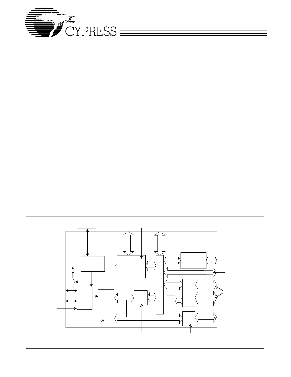
FX1
Address (16)
D+
D–
Integrated
full-speed XCVR
x20
VCC
PLL
1.5k
connected for
enumeration
USB
XCVR
Enhanced USB core
Simplifies 8051 code
/0.5
/1.0
/2.0
CY
Smart
USB
Engine
8051 Core
12/24/48 MHz,
four clocks/cycle
16 KB
RAM
“Soft Configuration”
Easy firmware changes
Figure 1-1. Block Diagram
Cypress Semiconductor Corporation • 3901 North First Street • San Jose, CA 95134 • 408-943-2600
Document #: 38-08039 Rev. *B Revised February 14, 2005
Data (8)
Additional I/Os (24)
GPIF
ECC
Address (16) / Data Bus (8)
FIFO
FIFO and endpoint memory
(master or slave operation)
Master
4 kB
2
I
C
Abundant I/O
including two USARTS
ADDR (9)
RDY (6)
CTL (6)
8/16
General
programmable I/F
to ASIC/DSP or bus
standards such as
ATAPI, EPP, etc.
Up to 96 MBytes/s
burst rate
Page 2

CY7C64713/14
2.0 Functional Description
EZ-USB FX1 (CY7C64713/4) is a full-speed highly
integrated, USB microc ontroller. By integrating the USB transceiver , serial interface engine (SIE), enhanc ed 8051 microcontroller, and a programmable peripheral interface in a single
chip, Cypress has created a ve ry cost-effecti ve solution tha t
provides superior time-to-market advantages.
Because it incorporat es the USB transcei ver , the EZ-USB FX1
is more economi cal, prov iding a small er footprin t soluti on than
USB SIE or external transceiver implementations. With
EZ-USB FX1, the Cypress Smart SIE handles most of the USB
protocol in hardwa re, freeing the embed ded microcontroll er for
application-specific functions and decreasing development
time to ensure USB compatibility.
The General Programmable Interface (GPIF) and Master/
Slave Endpoint FIFO (8- or 16-bit data bus) provides an easy
and glueless interface to popular interfaces such as
UTOPIA, EPP, PCMCIA, and most DSP/processors.
Three lead-free packages are defined for the family: 56 QFN,
100 TQFP, and 128 TQFP.
ATA,
3.0 Applications
• DSL modems
• ATA interface
• Memory card readers
• Legacy conversion devices
• Home PNA
• Wireless LA N
• MP3 players
• Networking
The “Reference Designs” section of the cypress website
provides additional tools for typical USB applications. Each
reference design comes complete with firmware source and
object code, schematics, and documentation. Please visit
http://www.cypress.com for more information.
4.0 Functional Overview
4.1 USB Signaling Speed
FX1 operates at one of the three rates defined in the USB
Specification Revision 2.0, dated April 27, 2000:
• Full speed, with a signaling bit rate of 12 Mbps.
FX1 does not support the low-speed signaling mode of 1.5
Mbps or the high-speed mode of 480 Mbps.
C1
4.2 8051 Microprocessor
The 8051 microprocessor embedded in the FX1 family has
256 bytes of register RAM, an expanded interrupt system,
three timer/counters, and two USARTs.
4.2.1 8051 Clock Frequency
FX1 has an on-chip oscillator circ uit that use s an external 24MHz (±100 ppm) crystal with the following characteristics:
• Parallel resonant
• Fundamental mode
• 500-µW drive level
• 12-pF (5% tolerance) load capacitors.
An on-chip PLL multiplies the 24-MHz oscillator up to 480
MHz, as required by the transceiver/PHY, and internal
counters divide it down for use as the 8051 clock. Th e de fau lt
8051 clock frequency is 12 MHz. The clock frequency of the
8051 can be changed by the 8051 through the CPUCS
register, dynamically.
The CLKOUT pin, which can be three-stated and inverted
using internal control bits, outputs the 50% duty cycle 8051
clock, at the selected 8051 clock frequency—48, 24, or 12
MHz.
4.2.2 USARTS
FX1 contains two standard 8051 USARTs, addressed via
Special Function Register (SFR) bits. The USART interface
pins are available on separate I/O pins, and are not multiplexed with port pins.
UART0 and UAR T1 can operate using an intern al clock at 23 0
KBaud with no more than 1% baud rate error. 230-KBaud
operation is achieved by an in ternally derived clock source that
generates overflow pulses at the appropriate time. The
internal clock adjus ts for the 8051 cloc k ra te (4 8, 2 4, 1 2 M Hz)
such that it always presents the correct frequency for 230KBaud operation.
4.2.3 Special Function Registers
Certain 8051 SFR addresses are populated to provide fast
access to critical FX1 functions. These SFR additions are
shown in Table 4-1. Bold type indicates non-standard,
enhanced 8051 registers . The two SFR ro ws that end wit h “0”
and “8” contain bit-addressable registers. The four I/O ports
A–D use the SFR addresses used in the standard 8051 for
ports 0–3, which are not implemented in FX1. Because of the
faster and more efficient SFR addressing, the FX1 I/O ports
are not addressable in extern al R AM space (using the MOVX
instruction).
24 MHz
C2
[1]
12 pf
20 × PLL
Figure 4-1. Crystal Configuration
Note:
1. 115-KBaud operation is also possible by programming the 8051 SMOD0 or SMOD1 bits to a “1” for UART0 and/or UART1, respectively.
Document #: 38-08039 Rev. *B Page 2 of 50
12 pf
12-pF capacitor values assumes a trace
capacitance of 3 pF per side on a four-layer FR4 PCA
Page 3
CY7C64713/14
4.3 I2C Bus
FX1 supports the I2C bus as a master only at 100/400 KHz.
SCL and SDA pins have open-drain outputs and hysteresis
inputs. These signals must be pulled up to 3.3V, even if no I
4.4 Buses
All packages: 8- or 16-bit “FIFO” bidirectional data bus, multiplexed on I/O ports B and D. 128-pin package: adds 16-bit
2
C
output-only 8051 address bus, 8-bit bidirectional data bus.
device is connected.
Table 4-1. Special Function Registers
x8x 9x Ax Bx CxDxExFx
0
1SP EXIF
2DPL0 MPAGE
3DPH0
4 DPL1
5 DPH1
6 DPS
IOA IOB IOC IOD SCON1 PSW ACC B
INT2CLR IOE SBUF1
INT4CLR OEA
OEB
OEC
OED
OEE
7PCON
8 TCON SCON0 IE IP T2CON EICON EIE EIP
9 TMOD SBUF0
ATL0AUTOPTRH1 EP2468STAT EP01STAT RCAP2L
BTL1AUTOPTRL1 EP24FIFOFLGS GPIFTRIG RCAP2H
CTH0reserved EP68FIFOFLGS TL2
DTH1AUTOPTRH2 GPIFSGLDATH TH2
E CKCON AUTOPTRL2 GPIFSGLDATLX
F reserved AUTOPTRSETUP GPIFSGLDATLNOX
4.5 USB Boot Methods
During the power-up sequence, internal logic checks the I2C
port for the connection of an EEPROM whose first byte is
either 0xC0 or 0x C 2. I f f ou n d, it us es th e V ID/ PI D/ D ID val u es
in the EEPROM in place of the internally stored value s (0xC0),
or it boot-loads the EEPROM contents into internal RAM
(0xC2). If no EEPROM is detected, FX1 enumerates using
internally stored descriptors. The default ID values for FX1 are
VID/PID/DID (0x04B4, 0x6473, 0xAxxx where xxx=Chip
revision).
[2]
Table 4-2. Default ID Values for FX1
Default VID/PID/DID
Vendor ID 0x04B4 Cypress Semiconductor
Product ID 0x6473 EZ-USB FX1
Device
release
0xAnnn Depends chip revision (nnn = chip
revision where first silicon = 001)
4.6 ReNumeration™
Because the FX1’s configuration is soft, one chip can take on
the identities of multiple distinct USB devices.
When first plugged into USB, the FX1 enumerates automatically and download s firmwa re and U SB descr iptor t ables over
the USB cable. Next, the FX1 enumerates again, this time as
Note:
2. The I
2
C bus SCL and SDA pins must be pulled up, even if an EEPROM is not connected. Otherwise this detection method does not work properly.
a device defined by the downloaded information. This
patented two-step process, called ReNumeration, happens
instantly when the device is plugged in, with no hint that the
initial download step has occurred.
Two control bits in the USBCS (USB Control and Status)
register control the ReNumeration process: DISCON and
RENUM. To simulate a USB disconnect, the firmware sets
DISCON to 1. To reconnect, the firmware clears DISCON to 0.
Before reconnecting, the firmware sets or clears the RENUM
bit to indicate wh ether the firm ware or the Default U SB Device
will handle devi ce reques ts ov er end point zer o: if REN UM = 0,
the Default USB Device wil l handle device requ ests; if RENUM
= 1, the firmware will.
4.7 Bus-powered Applications
The FX1 fully supports bus-powered designs by enumerating
with less than 100 mA as required by the USB specification.
4.8 Interrupt System
4.8.1 INT2 Interrupt Request and Enable Registers
FX1 implements an autovector feature for INT2 and INT4.
There are 27 INT2 (USB) vectors, and 14 INT4 (FIFO/GPIF)
vectors. See EZ-USB Technical Reference Manual (TRM) for
more details.
Document #: 38-08039 Rev. *B Page 3 of 50
Page 4

CY7C64713/14
4.8.2 USB-Interrupt Autovectors
The main USB interrupt is shared by 27 interrupt sources. To
save the code and processing time that normally would be
required to identify the individual USB interrupt source, the
FX1 provides a second level of interrupt vectoring, called
Autovectoring. When a USB interrupt is asserted, the FX1
pushes the program counter onto its stack then jumps to
address 0x0043, where it expects to find a “jump” instruction
to the USB Interrupt service routine.
The FX1 jump instruction is encoded as shown in Table 4-3.
If Autovectoring is enabled (AV2EN = 1 in the INTSETUP
register), the FX1 substitutes its INT2VEC byte. Therefore, if
Table 4-3. INT2 USB Interrupts
USB INTERRUPT TABLE FOR INT2
Priority INT2VEC Value Source Notes
1 00 SUDAV Setup Data Available
2 04 SOF Start of Frame
3 08 SUTOK Setup Token Received
4 0C SUSPEND USB Suspend request
5 10 USB RESET Bus reset
6 14 reserved
7 18 EP0ACK FX1 ACK’d the CONTROL Handshake
8 1C reserved
9 20 EP0-IN EP0-IN ready to be loaded with data
10 24 EP0-OUT EP0-OUT has USB data
11 28 EP1-IN EP1-IN ready to be loaded with data
12 2C EP1-OUT EP1-OUT has USB data
13 30 EP2 IN: buffer available. OUT: buffer has data
14 34 EP4 IN: buffer available. OUT: buffer has data
15 38 EP6 IN: buffer available. OUT: buffer has data
16 3C EP8 IN: buffer available. OUT: buffer has data
17 40 IBN IN-Bulk-NAK (any IN endpoint)
18 44 reserved
19 48 EP0PING EP0 OUT was Pinged and it NAK’d
20 4C EP1PING EP1 OUT was Pinged and it NAK’d
21 50 EP2PING EP2 OUT was Pinged and it NAK’d
22 54 EP4PING EP4 OUT was Pinged and it NAK’d
23 58 EP6PING EP6 OUT was Pinged and it NAK’d
24 5C EP8PING EP8 OUT was Pinged and it NAK’d
25 60 ERRLIMIT Bus errors exceeded the programmed limit
26 64
27 68 reserved
28 6C reserved
29 70 EP2ISOERR ISO EP2 OUT PID sequence error
30 74 EP4ISOERR ISO EP4 OUT PID sequence error
31 78 EP6ISOERR ISO EP6 OUT PID sequence error
32 7C EP8ISOERR ISO EP8 OUT PID sequence error
the high byte (“page”) of a jump-table address is preloaded at
location 0x0044, the automatically-inserted INT2VEC byte at
0x0045 will direct the jum p to the correct addres s out of the 27
addresses within the page.
4.8.3 FIFO/GPIF Interrupt (INT4)
Just as the USB Inte rrupt is sha red am ong 2 7 ind ividual USBinterrupt sources, the FIFO/GPIF interrupt is shared among 14
individual FIFO/GPIF sources. The FIFO/GPIF Interrupt, like
the USB Interrupt, can employ autovectoring. Table 4-4 shows
the priority and INT4VEC values for the 14 FIFO/GPIF
interrupt sources.
Document #: 38-08039 Rev. *B Page 4 of 50
Page 5

Table 4-4. Individual FIFO/GPIF Interrupt Sources
Priority INT4VEC Value Source Notes
1 80 EP2PF Endpoint 2 Programmable Flag
2 84 EP4PF Endpoint 4 Programmable Flag
3 88 EP6PF Endpoint 6 Programmable Flag
4 8C EP8PF Endpoint 8 Programmable Flag
5 90 EP2EF Endpoint 2 Empty Flag
6 94 EP4EF Endpoint 4 Empty Flag
7 98 EP6EF Endpoint 6 Empty Flag
8 9C EP8EF Endpoint 8 Empty Flag
9 A0 EP2FF Endpoint 2 Full Flag
10 A4 EP4FF Endpoint 4 Full Flag
11 A8 EP6FF Endpoint 6 Full Flag
12 AC EP8FF Endpoint 8 Full Flag
13 B0 GPIFDONE GPIF Operation Complete
14 B4 GPIFWF GPIF Waveform
CY7C64713/14
If Autovectoring is enabled (AV4EN = 1 in the INTSETUP
4.9 Reset and Wakeup
register), the FX1 substitutes its INT4VEC byte. Therefore, if
the high byte (“page”) of a jump-table address is preloaded at
location 0x0054, the automatically-inserted INT4VEC byte at
0x0055 will direct the jump to the c orrect address out of the 14
addresses within the page. When the ISR occurs, the FX1
pushes the program counter onto its stack then jumps to
address 0x0053, where it expects to find a “jump” instruction
to the ISR Interrupt service routine.
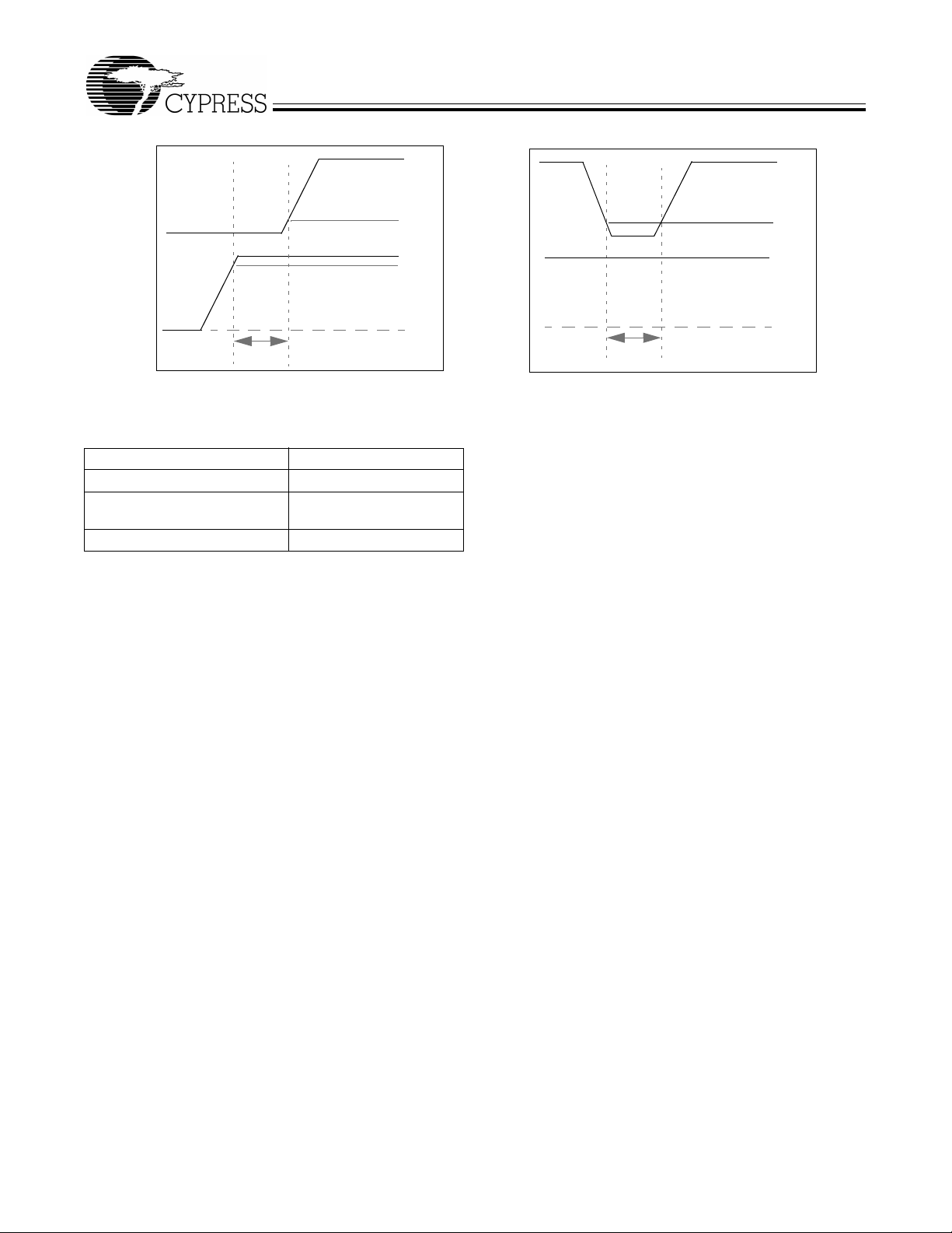
4.9.1 Reset Pin
The input pin, RESET#, will res et the FX1 when asserted. This
pin has hysteresis and is active LOW. When a crystal is used
with the CY7C64713/4 the reset period must allow for the
stabilization of the crystal and the PLL. This reset period
should be approximately 5 ms after VCC has reached 3.0
Volts. If the crystal input pin is driven by a clock signal the
internal PLL stabilizes in 200 µs after VCC has reached
[3]
. Figure 4-2 shows a power on reset condition and a
3.0V
reset applied during operation. A power on reset is defined as
the time reset is asserted while power is being applied to the
circuit. A powered reset is defined to be when the FX1 has
previously been powered on and operating and the RESET#
pin is asserted.
Cypress provides an application note which describes and
recommends power on res et implementation and can be found
on the Cypress web site. Wh ile the appl ication no te discus ses
the FX2, the information provid ed app lies a lso to the FX1. F or
more infor mation on reset implem entation for th e FX2 fa mily
of products visit the http://www.cypress.com.
Note:
3. If the external clock is powered at the same time as the CY7C64713/4 and has a stabilization wait period, it must be added to the 200
µs.
Document #: 38-08039 Rev. *B Page 5 of 50
Page 6
CY7C64713/14
RESET#
V
IL
3.3V
3.0V
VCC
0V
T
RESET
Power on Reset
Figure 4-2. Reset Timing Plots
Table 4-5. Reset Timing Values
Condition T
RESET
Power-On Reset with crystal 5 ms
Power-On Reset with external
200 µs + Clock stability time
clock
Powered Reset 200 µs
4.9.2 Wakeup Pins
The 8051 puts it self and the rest of the chip into a pow er-down
mode by setting PCON.0 = 1. This stops the oscillator and
PLL. When WAKEUP is asserted by external logic, the oscillator restarts, after the PLL stabilizes, and then the 8051
receives a wakeup interrupt. This applies whether or not FX1
is connected to the USB.
The FX1 exits the power-down (USB suspend) state using one
of the following methods:
• USB bus activity (if D+/D– lines are left floating, noise on
these lines may indicate activity to the FX1 and initiate a
wakeup).
• External logic asserts the WAKEUP pin
• External logic asserts the PA3/WU2 pin.
The second wakeup pin, WU2, can also be configured as a
general purpose I/O pin. This allows a simple external R-C
network to be used as a periodic wakeup source. Note that
WAKEUP is by default active low.
4.10 Program/Data RAM
RESET#
V
IL
3.3V
VCC
0V
T
RESET
Powered Reset
access it as both program and data memory. No USB control
registers appear in this space.
Two memory maps are shown in the following diagrams:
Figure 4-3 Internal Code Memory, EA = 0
Figure 4-4 External Code Memory, EA = 1.
4.10.2 Internal Code Memory, EA = 0
This mode implements the internal 16-KByte block of RAM
(starting at 0) as combined code and data memory. When
external RAM or ROM is added, the external read and write
strobes are suppressed for memory spaces that exist inside
the chip. This allows the user to connect a 64-KByte memory
without requiring address decodes to keep clear of internal
memory spaces.
Only the internal 16 KBytes an d scratch pad 0. 5 KBytes RAM
spaces have the following access:
• USB download
• USB upload
• Setup data pointer
2
C interface boot load.
• I
4.10.3 External Code Memory, EA = 1
The bottom 16 KBytes of program memory is external, and
therefore the bottom 16 KBytes of internal RAM is accessible
only as data memory.
4.10.1 Size
The FX1 has 16 KBytes of inter nal progr am/ dat a RAM, w here
PSEN#/RD# signals are internally ORed to allow the 8051 to
Document #: 38-08039 Rev. *B Page 6 of 50
Page 7
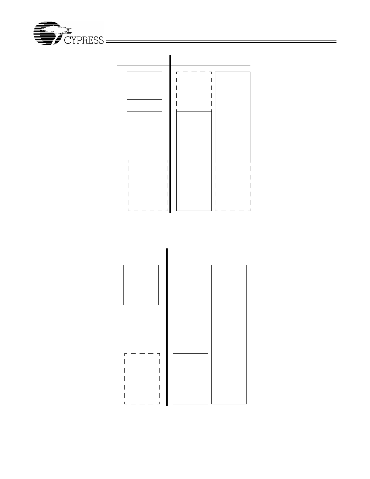
Inside FX1 Outside FX1
FFFF
4K FIFO buffers
E200
E1FF
0.5 KBytes RAM
Data (RD#,WR#)*
E000
3FFF
7.5 KBytes
USB regs and
(RD#,WR#)
(OK to populate
data memory
here—RD#/WR#
strobes are not
active)
40 KBytes
External
Data
Memory
(RD#,WR#)
48 KBytes
External
Code
Memory
(PSEN#)
CY7C64713/14
16 KBytes RAM
Code and Data
(PSEN#,RD#,WR#)*
0000
(Ok to populate
data memory
here—RD#/WR#
strobes are not
active)
Data Code
(OK to populate
program
memory here—
PSEN# strobe
is not active)
*SUDPTR, USB upload/download, I2C interface boot access
Figure 4-3. Internal Code Memory, EA = 0
Inside FX1 Outside FX1
FFFF
4K FIFO buffers
E200
E1FF
0.5 KBytes RAM
Data (RD#,WR#)*
E000
3FFF
7.5 KBytes
USB regs and
(RD#,WR#)
(OK to populate
data memory
here—RD#/WR#
strobes are not
active)
40 KBytes
External
Data
Memory
(RD#,WR#)
64 KBytes
External
Code
Memory
(PSEN#)
(Ok to populate
data memory
here—RD#/WR#
strobes are not
active)
Data Code
0000
16 KBytes
RAM
Data
(RD#,WR#)*
*SUDPTR, USB upload/download, I2C interface boot access
Figure 4-4. External Code Memory, EA = 1
Document #: 38-08039 Rev. *B Page 7 of 50
Page 8

4.11 Register Addresses
CY7C64713/14
FFFF
F000
EFFF
E800
E7FF
E7C0
E7BF
E780
E77F
E740
E73F
E700
E6FF
E500
E4FF
E480
E47F
E400
E3FF
E200
E1FF
E000
4 KBytes EP2-EP8
(8 x 512)
Not all Space is available
for all transfer types
2 KBytes RESERVED
64 Bytes EP1IN
64 Bytes EP1OUT
64 Bytes EP0 IN/OUT
64 Bytes RESERVED
8051 Addressable Registers
Reserved (128)
128 bytes GPIF Waveforms
Reserved (512)
512 bytes
8051 xdata RAM
buffers
(512)
4.12 Endpoint RAM
4.12.1 Size
• 3 × 64 bytes (Endpoints 0 and 1)
• 8 × 512 bytes (Endpoints 2, 4, 6, 8)
4.12.2 Organization
• EP0—Bidirectional endpoint zero, 64- byte buffer
• EP1IN, EP1OUT—64-byte buffers, bulk or interrupt
• EP2,4,6,8—Eight 512-byte bu ffers, bulk, inter rupt, or isoch-
ronous, of which only the transfer size is available.
EP4 and EP8 can be double buf fered, while EP2 an d 6 can
be either double, triple , or quad buffered. Regard less of the
physical size of the buffer, each endpo int buffer accomm odates only one full-speed packet. For bulk endpoints the
maximum number o f bytes it can accommoda te is 64, ev en
though the physical buffer size is 512 or 1024. For an
ISOCHRONOUS endpoint the maximum number of bytes
it can accommodate is 1023. For endpoint configuration
options, see Figure 4-5.
4.12.3 Setup Data Buffer
A separate 8-byte buffer at 0xE6B8-0xE6BF holds the Setup
data from a CONTROL transfer.
Document #: 38-08039 Rev. *B Page 8 of 50
Page 9
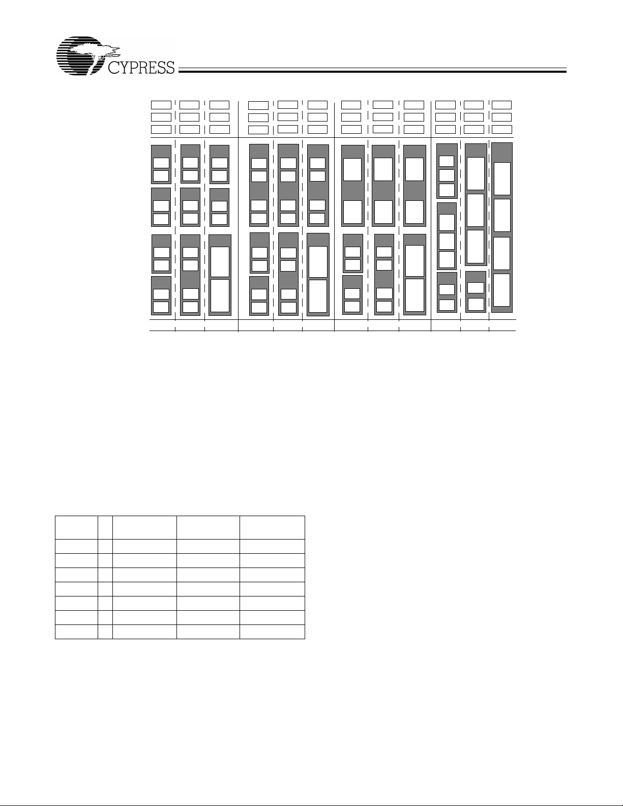
4.12.4 Endpoint Configurations
EP0 IN&OUT
EP1 IN
EP1 OUT
64
64
64
CY7C64713/14
64
64
64
64
64
64
64
64
64
64
64
64
64
64
64
64
64
64
64
64
64
64
64
64
64
64
64
64
64
64
64
64
64
EP2
EP2
64
64
EP4
64
64
EP6
64
64
EP8
64
64
1
64
64
EP4
64
64
EP6
64
64
64
64
2
EP2
64
64
EP4
64
64
EP6
1023
1023
3
EP2
64
64
64
64
EP6
64
64
EP8
64
64
4
EP2
64
64
64
64
EP6
64
64
64
64
5
Figure 4-5. Endpoint Configuration
Endpoints 0 and 1 are the same for every configuration.
Endpoint 0 is the only CONTROL endpoint, and endpoint 1 can
be either BULK or INTERRUPT. The endpoint buffers can be
configured in any 1 of the 12 configurations shown in the
vertical columns. In ful l-s pe ed, BU LK m od e use s onl y the firs t
64 bytes of ea ch buffer, even though mem ory exists for t he
allocation of the isochronous transfers in BULK mode the
unused endpoint buf fer sp ace is not av ailab le for other ope rations. An example endpoint configuration would be:
EP2—1023 double buffere d; EP6—64 quad buffered (column
8).
4.12.5 Default Alternate Settings
Table 4-6. Default Alternate Settings
[4, 5]
Alternate
Setting 0 1 2 3
ep0 64 64 64 64
ep1out 0 64 bulk 64 int 64 int
ep1in 0 64 bulk 64 int 64 int
ep2 0 64 bulk out (2×)64 int out (2×) 64 iso out (2×)
ep4 0 64 bulk out (2×)64 bulk out (2×) 64 bulk out (2×)
ep6 0 64 bulk in (2×) 64 int in (2×) 64 iso in (2×)
ep8 0 64 bulk in (2×) 64 bulk in (2×) 64 bulk in (2×)
EP2
64
64
64
64
EP6
1023
1023
6
EP2
1023
1023
EP6
64
64
EP8
64
64
7
EP2
1023
1023
EP6
64
64
64
64
8
EP2
1023
1023
EP6
1023
1023
9
EP2
64
64
64
EP6
64
64
64
EP8
64
64
10
EP2
1023
1023
1023
1023
EP8
64
64
11
EP2
1023
1023
1023
1023
12
are controlled by F IFO control signa ls (such as IFCLK, SL CS#,
SLRD, SL WR, SLOE, PKTEND, and flag s). The usable size of
these buffers depend on the USB transfer mode as describe d
in Section 4.12.2.
In operation , so me of th e eig ht RAM bl ocks fill or em pty from
the SIE, while the others are connected to the I/O transfer
logic. The trans fer logic takes two forms, the G PIF for internally
generated control signals, or the slave FIFO interface for
externally controlled transfers.
4.13.2 Master/Slave Control Signals
The FX1 endpoint FIFOS are im plemente d as eight physica lly
distinct 256x16 RAM blocks. The 8051/SIE can switch any of
the RAM blocks between tw o domains, th e USB (SIE) domain
and the 8051-I/O Un it do ma in. This switching is don e virtually
instantaneously, giving essentially zero transfer time between
“USB FIFOS” and “Slave FIFOS.” Since they are phy sically the
same memory, no bytes are actually transferred between
buffers.
4.13 External FIFO Interface
4.13.1 Architecture
The FX1 slave FIF O arc hitecture has eight 5 12- byte blocks in
the endpoint RA M tha t d ire ct l y s er v e a s FIF O m em or i e s, a nd
Notes:
4. “0” means “not implemented.”
5. “2×” means “double buf fered.”
Document #: 38-08039 Rev. *B Page 9 of 50
Page 10

CY7C64713/14
At any given time, some RAM blocks are filling/emptying with
USB data under SIE control, while other RAM blocks are
available to the 8051 and/or the I/O control unit. The RAM
blocks operate as single-port in the USB domain, and dualport in the 8051-I/O domai n. Th e bl oc ks can be c onf igu r ed a s
single, double, triple, or quad buffered as previously shown.
The I/O control unit implements either an internal-master (M
for master) or external-master (S for Slave) interface.
In Master (M) mode, the GPIF internally controls
FIFOADR[1..0] to select a FIFO. The RDY pi ns (two in the 56pin package, six in the 10 0-pin and 128-pin p ack ages) ca n be
used as flag inputs from an external FIFO or other logic if
desired. The GPIF can be r un from ei ther an internal ly derive d
clock or externally supplied clock (IFCLK), at a rate that
transfers data up to 96 Megabytes/s (48-MHz IFCLK with 16bit interface).
In Slave (S) mode, the FX1 accept s either an interna lly derived
clock or externally supplied clock (IFCLK, max. frequency 48
MHz) and SLCS#, SLRD, SLWR, SLOE, PKTEND signals
from external logic. When using an external IFCLK, the
external clock mus t be present b efore switch ing to the ext ernal
clock with the I FCLKSRC bit . Each endpoint can individ ually
be selected for byte or word operation by an internal configuration bit, and a Slave FIFO Output Enable signal SLOE
enables data of the sel ec ted width. External logic mu st in su re
that the output enable sign al is inac tive when writing data to a
slave FIFO. The slave interface can also operate asynchronously, where the SLRD and SLWR signals act directly as
strobes, rather than a cloc k qual ifier as in synchr onous m ode.
The signals SLRD, SLWR, SLOE and PKTEND are gated by
the signal SLCS#.
4.13.3 GPIF and FIFO Clock Rates
An 8051 register bit selects one of two frequencies for the
internally suppl ied i nterfac e cloc k: 30 MHz a nd 48 MHz. Alt ernatively, an externally supplied clock of 5 MHz–48 MHz
feeding the IFCLK pin can be used as the interface clock.
IFCLK can be configured to function as an output clock when
the GPIF and FIFOs are internally clocked. An output enable
bit in the IFCONFIG register turns this clock output off, if
desired. Another bit within the IFCONFIG register will invert
the IFCLK signal whether internally or externally sourced.
4.14 GPIF
The GPIF is a flexible 8- or 16-bit parallel interface driven by a
user-programmable finite state machine. It allows the
CY7C64713/4 to perform local bus mastering, and can
implement a wide variety of protocols such as ATA interface,
printer parallel port, and Utopia.
The GPIF has six programmable control outputs (CTL), nine
address outputs (GPIFADRx), and six general-purpose ready
inputs (RDY). The data bus width can be 8 or 16 bits. Each
GPIF vector defines the s tate of the control outputs, and determines what stat e a ready input (or multi ple inputs) must be
before proceeding. The GPIF vector can be programmed to
advance a FIFO to the next data value, advance an address,
etc. A sequence of the GPIF vectors make up a single
waveform that will be executed to perform the desired data
move between the FX1 and the external device.
Document #: 38-08039 Rev. *B Page 10 of 50
4.14.1 Six Control OUT Signals
The 100- and 128-pin packages bring out all six Control Output
pins (CTL0-CTL5). The 8051 prog rams the GPIF unit to define
the CTL waveforms. The 56-pin package brings out three of
these signals, CTL0–CTL2. CTLx waveform edges can be
programmed to make transitions as fast as once per clock
(20.8 ns using a 48-MHz clock).
4.14.2 Six Ready IN Signals
The 100- and 128-pin packages bring out all six Ready in puts
(RDY0–RDY5). The 8051 programs the GPIF unit to test the
RDY pins for GPIF branching. The 56-pin package brings out
two of these signals, RDY0–1.
4.14.3 Nine GPIF Address OUT Signals
Nine GPIF address line s are avai lable in th e 100 - and 128-pi n
packages, GPIFADR[8..0]. The GPIF address lines allow
indexing through up to a 512-byte block of RAM. If more
address lines are needed, I/O port pins can be used.
4.14.4 Long Transfer Mode
In master mode, t he 8051 app ropriately sets G PIF transac tion
count registers (GPIFTCB3, GPIFTCB2, GPIFTCB1, or
GPIFTCB0) for unattended trans fers of up to 2
The GPIF automatical ly thro ttles d ata flow to preven t under or
overflow until the full number of requested transactions
complete. The GPIF decrements the value in these registers
to represent the current status of the transaction.
32
transactions.
4.15 ECC Generation
The EZ-USB FX1 can calculate ECCs (Error-Correcting
Codes) on da ta that passes acros s its GPIF or Slave F IFO
interfaces. There are two ECC configurations: Two ECCs,
each calculated o ver 256 bytes (Sm artMedia™ S tandard); and
one ECC calculated over 512 bytes.
The ECC can correct any one-bit error or detect any two-bit
error.
Note: To use the ECC logic, the GPIF or Slav e FIFO inte rface
must be configured for byte-wide operation.
4.15.1 ECC Implementation
The two ECC configurations are selected by the ECCM bit:
4.15.1.1 ECCM = 0
Two 3-byte ECCs, each calculated over a 256-byte block of
data. This configuration conforms to the SmartMedia
Standard.
Write any value to ECCRESET, then pass data across the
GPIF or Slave FIFO interface. The ECC for the first 256 bytes
of data will be c alculated and s tored in ECC1. T he ECC for the
next 256 bytes will be stored in ECC2. After the second ECC
is calculated, the va lues in the ECCx reg isters will not ch ang e
until ECCRESET is written again, even if more data is subsequently passed across the interface.
4.15.1.2 ECCM=1
One 3-byte ECC calculated over a 512-byte block of data.
Write any value to ECCRESET then pass data across the
GPIF or Slave FIFO interface. The ECC for the first 512 bytes
of data will be calculated and stored in ECC1; EC C2 is unused.
After the ECC is calcu lated, the v alue in ECC 1 will not ch ange
Page 11

CY7C64713/14
until ECCRESET is written again, even if more data is subsequently passed across the interface
4.18.2 I
At power-on reset the I
2
C Interface Boot Load Access
2
C interface boot loader will load the
VID/PID/DID configuration bytes and up to 16 KBytes of
4.16 USB Uploads and Downloads
The core has the abilit y to dire ctly edi t the data content s of the
internal 16 KByte RAM and of the internal 512-byte scratch
pad RAM via a vendor-specific command. This capability is
normally used when “soft” downloading user code and is
available only to and from internal RAM, only when the 8051
is held in reset. The avai lable RAM spac es are 16 KBytes from
0x0000–0x3FFF (code/data) and 512 bytes from
0xE000–0xE1FF (scratch pad data RAM).
[6]
4.17 Autopointer Access
FX1 provides two identical autopointers. They are similar to
the internal 8051 dat a poi nter s, bu t with an ad dit ion al fe ature:
they can optional ly increment after ev ery memory access. This
capability is available to and from both internal and external
RAM. The autopointers are av ailable in external FX1 regist ers,
under control of a mode bit (AUTOPTRSETUP.0). Using the
external FX1 autopoint er access (at 0xE67B – 0xE67C) allows
the autopointer t o acces s al l RAM, int ernal and exte rnal to the
program/data. The availa ble RA M sp aces are 16 KByte s from
0x0000–0x3FFF and 512 bytes from 0xE000–0xE1FF. The
8051 will be in reset. I
2
C interface boot loads only occur after
power-on reset.
2
4.18.3 I
The 8051 can control peripherals connected to the I
using the I2CTL an d I2DA T regis ters. FX1 provid es I
control only, it is never an I
C Interface General Purpose Access
2
C slave.
2
4.19 Compatible with Previous Generation
EZ-USB FX2
The EZ-USB FX1 is fit/form/function-upgradable to the EZUSB FX2LP. This makes for a easy transition for designers
wanting to upgrade their systems from full-speed to the highspeed designs. The pinout and package selection are
identical, and all of the firmware developed for the FX1 will
function in the FX2LP with proper addition of High Speed
descriptors and speed switching code.
part. Also, the autopointers can point to any FX1 register or
endpoint buff er space. When au topointer ac cess to exte rnal
memory is enabled, location 0xE67B and 0xE67C in XDATA
and code space cannot be used.
5.0 Pin Assignments
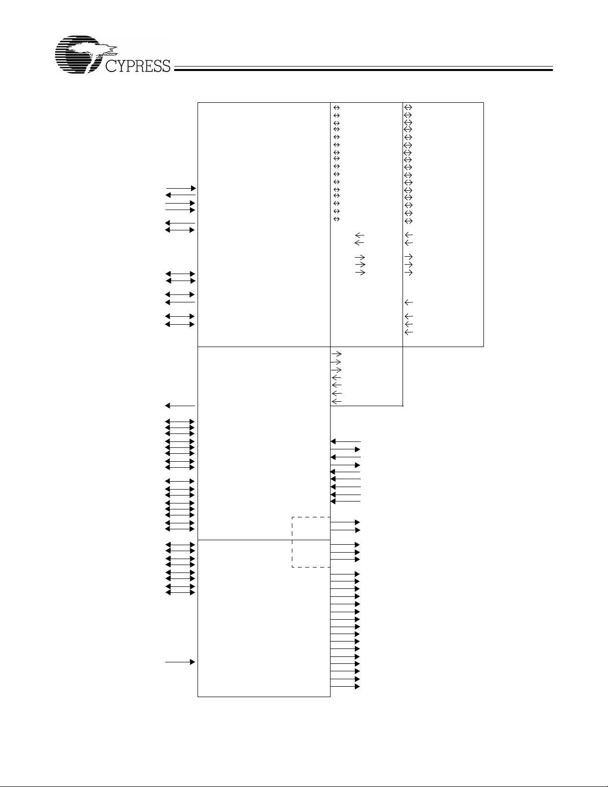
Figure 5-1 identifies all signals for the three package types.
The following pages illustrate the indiv idual pin diagrams , plus
4.18 I2C Controller
FX1 has one I2C port that is driv en by two internal controllers,
one that automatically operates at boot time to load
VID/PID/DID and configuration information, and another that
the 8051, once running, uses to control external I
2
C port operates in master mode only.
The I
4.18.1 I
The I
2
C Port Pins
2
C- pins SCL and SDA must have external 2.2-kΩ pullup resistors even if no EEPROM is connected to the FX1.
External EEPROM device address pins must be configured
properly. See Table 4-7 for configuring the device address
pins.
Table 4-7. Strap Boot EEPROM Address Lines to These
Values
Bytes Example EEPROM A2 A1 A0
16 24LC00
[7]
N/A N/A N/A
128 24LC01 0 0 0
256 24LC02 0 0 0
4K 24LC32 0 0 1
8K 24LC64 0 0 1
16K 24LC128 0 0 1
2
C devices.
a combination diagra m showin g which of the full set of signal s
are available in the 128-, 100-, and 56-pin packages.
The signals on t he lef t edge of t he 56-pin packa ge in Figure 5-
1 are common to all versions in the FX1 family. Three modes
are availabl e in al l packa ge ve rsion s: Por t, GP IF mast er, and
Slave FIFO. These modes defi ne the signals on the right edge
of the diagram. The 8051 select s the in terface m ode usin g the
IFCONFIG[1:0] register bits. Port mod e is the power-on de fault
configuration.
The 100-pin pa ckage adds func tional ity to the 56 -pin p ack age
by adding these pins:
• PORTC or alternate GPIFADR[7:0] address signals
• PORTE or alternate GPIFADR[8] address signal and seve n
additional 8051 signals
• Three GPIF Control s i gnals
• Four GPIF Ready signals
• Nine 8051 signals (two USARTs, three timer inputs,
INT4,and INT5#)
• BKPT, RD#, WR#.
The 128-pin package adds the 8051 address and data buses
plus control sign als. Note th at two of the required s ignals, RD #
and WR#, are present in the 100-pin version. In the 100-pin
and 128-pin versions, an 8051 control bit can be set to pulse
the RD# and WR# pins when the 8051 reads from/writes to
PORTC.
Notes:
6. After the data has been downloaded from the host, a “loader” can execute from internal RAM in order to transfer downloaded data to external memory.
7. This EEPROM does not have address pins.
2
C bus
C master
Document #: 38-08039 Rev. *B P age 11 of 50
Page 12
Port GPIF Master Slave FIFO
XTALIN
XTALOUT
RESET#
WAKEUP#
SCL
SDA
T0OUT
T1OUT
IFCLK
CLKOUT
DPLUS
DMINUS
56
100
BKPT
PORTC7/GPIFADR7
PORTC6/GPIFADR6
PORTC5/GPIFADR5
PORTC4/GPIFADR4
PORTC3/GPIFADR3
PORTC2/GPIFADR2
PORTC1/GPIFADR1
PORTC0/GPIFADR0
PE7/GPIFADR8
PE6/T2EX
PE5/INT6
PE4/RxD1OUT
PE3/RxD0OUT
PE2/T2OUT
PE1/T1OUT
PE0/T0OUT
D7
D6
D5
D4
D3
D2
D1
D0
128
EA
PD7
PD6
PD5
PD4
PD3
PD2
PD1
PD0
PB7
PB6
PB5
PB4
PB3
PB2
PB1
PB0
INT0#/PA0
INT1#/PA1
PA2
WU2/PA3
PA4
PA5
PA6
PA7
RxD0
TxD0
RxD1
TxD1
INT4
INT5#
T2
T1
T0
RD#
WR#
CS#
OE#
PSEN#
A15
A14
A13
A12
A11
A10
A9
A8
A7
A6
A5
A4
A3
A2
A1
A0
FD[15]
FD[14]
FD[13]
FD[12]
FD[11]
FD[10]
FD[9]
FD[8]
FD[7]
FD[6]
FD[5]
FD[4]
FD[3]
FD[2]
FD[1]
FD[0]
RDY0
RDY1
CTL0
CTL1
CTL2
INT0#/PA0
INT1#/PA1
PA2
WU2/PA3
PA4
PA5
PA6
PA7
CTL3
CTL4
CTL5
RDY2
RDY3
RDY4
RDY5
CY7C64713/14
FD[15]
FD[14]
FD[13]
FD[12]
FD[11]
FD[10]
FD[9]
FD[8]
FD[7]
FD[6]
FD[5]
FD[4]
FD[3]
FD[2]
FD[1]
FD[0]
SLRD
SLWR
FLAGA
FLAGB
FLAGC
INT0#/ PA0
INT1#/ PA1
SLOE
WU2/PA3
FIFOADR0
FIFOADR1
PKTEND
PA7/FLAGD/SLCS#
Figure 5-1. Signals
Document #: 38-08039 Rev. *B Page 12 of 50
Page 13
CY7C64713/14
103
104
105
106
107
108
109
110
111
112
113
114
115
116
117
118
119
120
121
122
123
124
125
126
127
128
PD1/FD9
PD2/FD10
PD3/FD11
INT5#
VCC
PE0/T0OUT
PE1/T1OUT
PE2/T2OUT
PE3/RXD0OUT
PE4/RXD1OUT
PE5/INT6
PE6/T2EX
PE7/GPIFADR8
GND
A4
A5
A6
A7
PD4/FD12
PD5/FD13
PD6/FD14
PD7/FD15
GND
A8
A9
A10
1
CLKOUT
2
VCC
3
GND
4
RDY0/*SLRD
5
RDY1/*SLWR
6
RDY2
7
RDY3
8
RDY4
9
RDY5
10
AVCC
11
XTALOUT
12
XTALIN
13
AGND
14
NC
15
NC
16
NC
17
AVCC
18
DPLUS
19
DMINUS
20
AGND
21
A11
22
A12
23
A13
24
A14
25
A15
26
VCC
27
GND
28
INT4
29
T0
30
T1
31
T2
32
*IFCLK
33
RESERVED
34
BKPT
35
EA
36
SCL
37
SDA
38
OE#
A3
A2
A1
A0
D7
D6
D5
102
101
100
99
98
97
96
95
94
93
92
91
90
89
88
87
86
85
84
83
82
81
80
79
78
77
76
75
74
73
72
71
70
69
68
67
66
65
PD0/FD8
*WAKEUP
VCC
RESET#
CTL5
GND
PA7/*FLAGD/SLCS#
PA6/*PKTEND
PA5/FIFOADR1
PA4/FIFOADR0
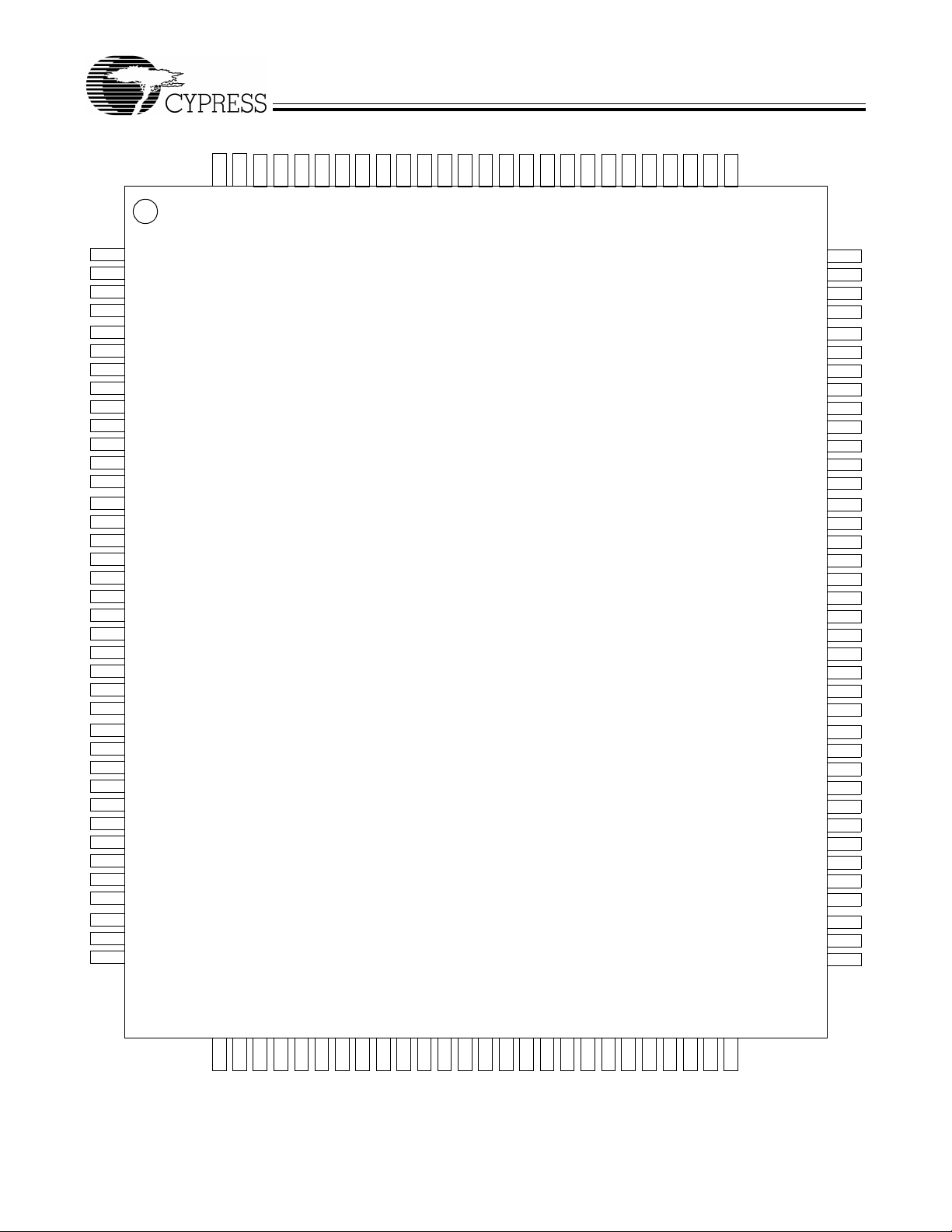
CY7C64713/4
128-pin TQFP
PA3/*WU2
PA2/*SLOE
PA1/INT1#
PA0/INT0#
VCC
GND
PC7/GPIFADR7
PC6/GPIFADR6
PC5/GPIFADR5
PC4/GPIFADR4
PC3/GPIFADR3
PC2/GPIFADR2
PC1/GPIFADR1
PC0/GPIFADR0
CTL2/*FLAGC
CTL1/*FLAGB
CTL0/*FLAGA
VCC
CTL4
CTL3
PSEN#
WR#
RD#
PB0/FD0
RXD0
TXD0
GND
VCC
CS#
VCC
RXD1
TXD1
PB4/FD4
PB7/FD7
PB6/FD6
PB5/FD5
GND
D0
D1
D2
D3
VCC
D4
PB3/FD3
PB2/FD2
PB1/FD1
GND
64
63
62
61
60
59
58
57
56
55
54
53
52
51
50
49
48
47
46
45
44
43
42
41
40
39
Figure 5-2. CY7C64713/4 128-pin TQFP Pin Assignment
* denotes pro grammable polarity
Document #: 38-08039 Rev. *B Page 13 of 50
Page 14
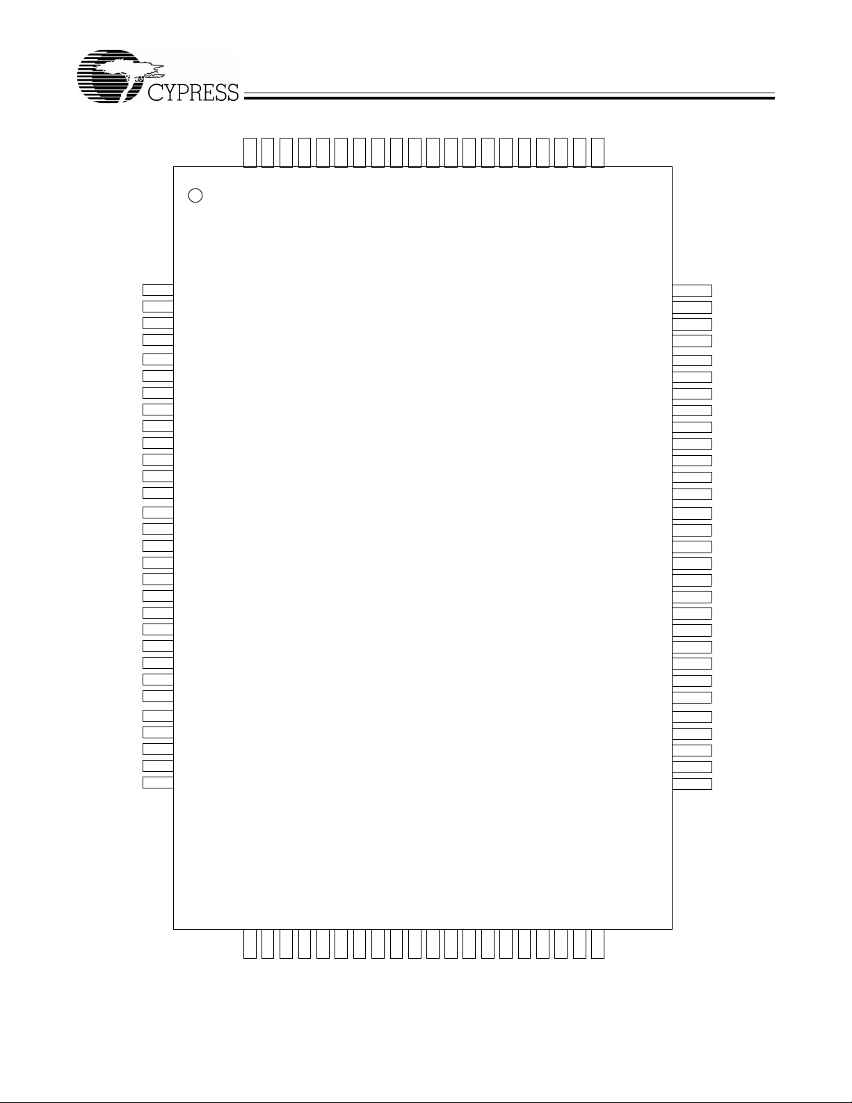
100
CLKOUT
99
PD7/FD15
GND
CY7C64713/14
81
82
83
84
85
86
87
88
89
90
91
92
93
94
95
96
97
98
PD1/FD9
PD2/FD10
PD3/FD11
INT5#
VCC
PE0/T0OUT
PE1/T1OUT
PE2/T2OUT
PE3/RXD0OUT
PE4/RXD1OUT
PE5/INT6
PE6/T2EX
PE7/GPIFADR8
GND
PD4/FD12
PD5/FD13
PD6/FD14
1
VCC
2
GND
3
RDY0/*SLRD
4
RDY1/*SLWR
5
RDY2
6
RDY3
7
RDY4
8
RDY5
9
AVCC
10
XTALOUT
11
XTALIN
12
AGND
13
NC
14
NC
15
NC
16
AVCC
17
DPLUS
18
DMINUS
19
AGND
20
VCC
21
GND
22
INT4
23
T0
24
T1
25
T2
26
*IFCLK
27
RESERVED
28
BKPT
29
SCL
30
SDA
CY7C64713/4
100-pin TQFP
PD0/FD8
*WAKEUP
VCC
RESET#
CTL5
GND
PA7/*FLAGD/SLCS#
PA6/*PKTEND
PA5/FIFOADR1
PA4/FIFOADR0
PA3/*WU2
PA2/*SLOE
PA1/INT1#
PA0/INT0#
VCC
GND
PC7/GPIFADR7
PC6/GPIFADR6
PC5/GPIFADR5
PC4/GPIFADR4
PC3/GPIFADR3
PC2/GPIFADR2
PC1/GPIFADR1
PC0/GPIFADR0
CTL2/*FLAGC
CTL1/*FLAGB
CTL0/*FLAGA
VCC
CTL4
CTL3
80
79
78
77
76
75
74
73
72
71
70
69
68
67
66
65
64
63
62
61
60
59
58
57
56
55
54
53
52
51
PB3/FD3
PB2/FD2
PB1/FD1
RD#
31
PB0/FD0
RXD0
TXD0
WR#
VCC
36
35
34
33
32
GND
VCC
41
40
39
38
37
RXD1
TXD1
43
42
PB4/FD4
44
PB7/FD7
PB6/FD6
PB5/FD5
GND
GND
VCC
50
49
48
47
46
45
Figure 5-3. CY7C64713/4 100-pin TQFP Pin Assignment
* denotes programmable polarity
Document #: 38-08039 Rev. *B Page 14 of 50
Page 15

CLKOUT/**PE1/T1OUT
CY7C64713/14
RDY0/*SLRD
RDY1/*SLWR
AVCC
XTALOUT
XTALIN
AGND
AVCC
DPLUS
DMINUS
AGND
VCC
GND
10
11
12
PD7/FD15
54
GND
53
50
51
52
CY7C64713/4
49
48
GND
VCC
55
56
1
2
3
4
5
6
7
47
PD1/FD9
46
PD2/FD10
PD3/FD11
PD4/FD12
PD5/FD13
PD6/FD14
56-pin QFN
8
9
PD0/FD8
45
*WAKEUP
44
VCC
43
RESET#
42
GND
41
PA7/*FLAGD/SLCS#
40
PA6/*PKTEND
39
PA5/FIFOADR1
38
PA4/FIFOADR0
37
PA3/*WU2
36
PA2/*SLOE
35
PA1/INT1#
34
PA0/INT0#
33
VCC
32
CTL2/*FLAGC
31
*IFCLK/**PE0/T0OUT
RESERVED
Document #: 38-08039 Rev. *B Page 15 of 50
13
14
16
15
SDA
SCL
Figure 5-4. CY7C64713/4 56-pin QFN Pin Assignment
18
17
PB0/FD0
VCC
* denotes programmable polarity
19
PB1/FD1
20
PB2/FD2
21
PB3/FD3
22
PB4/FD4
23
PB5/FD5
24
PB6/FD6
25
PB7/FD7
26
GND
27
VCC
28
GND
CTL1/*FLAGB
30
29
CTL0/*FLAGA
Page 16

CY7C64713/14
5.1 CY7C64713/4 Pin Definitions
Table 5-1. FX1 Pin Definitions
128
TQFP
100
TQFP
56
QFN Name Type
10 9 3 AVCC Power N/A Analog VCC. Connect this pin to 3.3V pow er source. T his signal prov ides
17 16 7 AVCC Power N/A Analog VCC. Conn ect this pin to 3.3V power s ource. This signal provid es
13 12 6 AGND Ground N/A Analog Ground. Connect to ground with as short a path as possible.
20 19 10 AGND Ground N/A Analog Ground. Connect to ground with as short a path as possible.
19 18 9 DMINUS I/O/Z Z USB D– Signal. Connect to the USB D– signal.
18 17 8 DPLUS I/O/Z Z USB D+ Signal. Connect to the USB D+ signal.
94 A0 Output L 8051 Address Bus. This bus is driven at all times. When the 8051 is
95 A1 Output L
96 A2 Output L
97 A3 Output L
117 A4 Output L
118 A5 Output L
119 A6 Output L
120 A7 Output L
126 A8 Output L
127 A9 Output L
128 A10 Output L
21 A11 Output L
22 A12 Output L
23 A13 Output L
24 A14 Output L
25 A15 Output L
59 D0 I/O/Z Z 8051 Data Bus. This bidirectional bus is high-impedance when inactive,
60 D1 I/O/Z Z
61 D2 I/O/Z Z
62 D3 I/O/Z Z
63 D4 I/O/Z Z
86 D5 I/O/Z Z
87 D6 I/O/Z Z
88 D7 I/O/Z Z
39 PSEN# Output H Program Store Enable. This active-LOW signal indicates an 8051 code
34 28 BKPT Output L Breakpoint. This pin goes active (HIGH) when the 8051 address bus
Note:
8. Unused inputs should not be left floating. Tie either HIGH or LOW as appropriate. Outputs should only be pulled up or down to ensure signals at power-up
and in standby. Note also that no pins should be driven while the device is powered down.
[8]
Default
Description
power to the analog section of the chip.
power to the analog section of the chip.
addressing internal RAM it reflects the internal address.
input for bus reads, and output for bus writes. The data bus is used for
external 8051 program and data memory. The data bus is active only for
external bus accesses, and is driven LOW in suspend.
fetch from external memory. It is active for program memory fetches from
0x4000–0xFFFF when th e EA pin is LOW, or from 0x0000–0xFFFF when
the EA pin is HIGH.
matches the BPADDRH/L registers and breakpoints are enabled in the
BREAKPT register (BPEN = 1). If the BPPULSE bit in the BREAKPT
register is HIGH, this sig nal pu lses HIGH for eigh t 12-/24 -/48-MH z cloc ks.
If the BPPULSE bit is LOW, the si gnal remain s HIGH until the 8051 cl ears
the BREAK bit (by writing 1 to it) in the BREAKPT register.
Document #: 38-08039 Rev. *B Page 16 of 50
Page 17

CY7C64713/14
Table 5-1. FX1 Pin Definitions (continued)
128
TQFP
Port A
100
TQFP
99 77 42 RESET# Input N/A Active LOW Reset. Resets the entire chip. See section 4.9 ”Reset and
35 EA Input N/A External Access. This pin determines where the 8051 fetches code
12 11 5 XTALIN Input N/A Crystal Input. Connect this signal to a 24-MHz parallel-resonant, funda-
11 10 4 XTALOUT Output N/A Crystal Output. Conne ct thi s sig nal to a 24- MHz pa rallel -resona nt, fun da-
1 100 54 CLKOUT O/Z 12
82 67 33 PA0 or
83 68 34 PA1 or
84 69 35 PA2 or
85 70 36 PA3 or
89 71 37 PA4 or
90 72 38 PA5 or
91 73 39 PA6 or
56
QFN Name Type
I/O/Z I
INT0#
I/O/Z I
INT1#
I/O/Z I
SLOE
I/O/Z I
WU2
I/O/Z I
FIFOADR0
I/O/Z I
FIFOADR1
I/O/Z I
PKTEND
[8]
Default
MHz
(PA0)
(PA1)
(PA2)
(PA3)
(PA4)
(PA5)
(PA6)
Description
Wakeup” on page 5 for more details.
between addresses 0x0000 and 0x3FFF. If EA = 0 the 8051 fetches this
code from its internal RAM. IF EA = 1 the 8051 fetches this code from
external memory.
mental mode crystal and loa d capacitor to GN D.
It is also correct to drive XTALIN with an external 24 MHz square wave
derived from anothe r clock sourc e. When driving from an extern al so urce,
the driving signal should be a 3.3V square wave.
mental mode crystal and loa d capacitor to GN D.
If an external clock is used to drive XTALIN, leave this pin open.
CLKOUT: 12-, 24- or 48-MHz clock, phase locked to the 24-MHz input
clock. The 8051 defaults to 12-MHz operation. The 8051 may three-state
this output by setting CPUCS.1 = 1.
Multiplexed pin whose function is selected by PORTACFG.0
PA0 is a bidirectional IO port pin.
INT0# is the active-LOW 8051 INT0 interrupt input signal, which is either
edge triggered (IT0 = 1) or level triggered (IT0 = 0).
Multiplexed pin whose function is selected by:
PORTACFG.1
PA1 is a bidirectional IO port pin.
INT1# is the active-LOW 8051 INT1 interrupt input signal, which is either
edge triggered (IT1 = 1) or level triggered (IT1 = 0).
Multiplexed pin whose function is selected by two bits:
IFCONFIG[1:0].
PA2 is a bidirectional IO port pin.
SLOE is an input-only output enable with programmable polarity (FIFOPIN-
POLAR.4) for the slave FIFOs connected to FD[7..0] or FD[15..0].
Multiplexed pin whose function is selected by:
WAKEUP.7 and OEA.3
PA3 is a bidirectional I/O port pin.
WU2 is an alternate source for USB Wake up, enabled by WU2EN bit
(WAKEUP.1) and polarity set by WU2POL (WAKEUP.4). If the 8051 is in
suspend and WU2EN = 1, a transition on this pin starts up the oscillator
and interrupts the 8051 to allow it to exit the suspend mode. Asserting this
pin inhibits the chip from suspending, if WU2EN=1.
Multiplexed pin whose function is selected by:
IFCONFIG[1..0].
PA4 is a bidirectional I/O port pin.
FIFOADR0 is an input-on ly a ddre ss s ele ct fo r th e s la ve FI FOs connected
to FD[7..0] or FD[15..0].
Multiplexed pin whose function is selected by:
IFCONFIG[1..0].
PA5 is a bidirectional I/O port pin.
FIFOADR1 is an input-on ly a ddre ss s ele ct fo r th e s la ve FI FOs connected
to FD[7..0] or FD[15..0].
Multiplexed pin whose function is selected by the IFCONFIG[1:0] bits.
PA6 is a bidirectional I/O port pin.
PKTEND is an input used to comm it the FIF O p acket data to the end po int
and whose polarity is programmable via FIFOPINPOLAR.5.
Document #: 38-08039 Rev. *B Page 17 of 50
Page 18

CY7C64713/14
Table 5-1. FX1 Pin Definitions (continued)
128
TQFP
Port B
PORT C
100
TQFP
92 74 40 PA7 or
44 34 18 PB0 or
45 35 19 PB1 or
46 36 20 PB2 or
47 37 21 PB3 or
54 44 22 PB4 or
55 45 23 PB5 or
56 46 24 PB6 or
57 47 25 PB7 or
72 57 PC0 or
73 58 PC1 or
74 59 PC2 or
75 60 PC3 or
76 61 PC4 or
56
QFN Name Type
I/O/Z I
FLAGD or
SLCS#
I/O/Z I
FD[0]
I/O/Z I
FD[1]
I/O/Z I
FD[2]
I/O/Z I
FD[3]
I/O/Z I
FD[4]
I/O/Z I
FD[5]
I/O/Z I
FD[6]
I/O/Z I
FD[7]
I/O/Z I
GPIFADR0
I/O/Z I
GPIFADR1
I/O/Z I
GPIFADR2
I/O/Z I
GPIFADR3
I/O/Z I
GPIFADR4
[8]
Default
(PA7)
(PB0)
(PB1)
(PB2)
(PB3)
(PB4)
(PB5)
(PB6)
(PB7)
(PC0)
(PC1)
(PC2)
(PC3)
(PC4)
Description
Multiplexed pin whose function is selected by the IFCONFIG[1:0] and
PORTACFG.7 bits.
PA7 is a bidirectional I/O port pin.
FLAGD is a programmable slave-FIFO output status flag signal.
SLCS# gates all other slave FIFO enable/strobes
Multiplexed pin whose function is selected by the following bits:
IFCONFIG[1..0].
PB0 is a bidirectional I/O port pin.
FD[0] is the bidirectional FIFO/GPIF data bus.
Multiplexed pin whose function is selected by the following bits:
IFCONFIG[1..0].
PB1 is a bidirectional I/O port pin.
FD[1] is the bidirectional FIFO/GPIF data bus.
Multiplexed pin whose function is selected by the following bits:
IFCONFIG[1..0].
PB2 is a bidirectional I/O port pin.
FD[2] is the bidirectional FIFO/GPIF data bus.
Multiplexed pin whose function is selected by the following bits:
IFCONFIG[1..0].
PB3 is a bidirectional I/O port pin.
FD[3] is the bidirectional FIFO/GPIF data bus.
Multiplexed pin whose function is selected by the following bits:
IFCONFIG[1..0].
PB4 is a bidirectional I/O port pin.
FD[4] is the bidirectional FIFO/GPIF data bus.
Multiplexed pin whose function is selected by the following bits:
IFCONFIG[1..0].
PB5 is a bidirectional I/O port pin.
FD[5] is the bidirectional FIFO/GPIF data bus.
Multiplexed pin whose function is selected by the following bits:
IFCONFIG[1..0].
PB6 is a bidirectional I/O port pin.
FD[6] is the bidirectional FIFO/GPIF data bus.
Multiplexed pin whose function is selected by the following bits:
IFCONFIG[1..0].
PB7 is a bidirectional I/O port pin.
FD[7] is the bidirectional FIFO/GPIF data bus.
Multiplexed pin whose function is selected by PORTCCFG.0
PC0 is a bidirectional I/O port pin.
GPIFADR0 is a GPIF address output pin.
Multiplexed pin whose function is selected by PORTCCFG.1
PC1 is a bidirectional I/O port pin.
GPIFADR1 is a GPIF address output pin.
Multiplexed pin whose function is selected by PORTCCFG.2
PC2 is a bidirectional I/O port pin.
GPIFADR2 is a GPIF address output pin.
Multiplexed pin whose function is selected by PORTCCFG.3
PC3 is a bidirectional I/O port pin.
GPIFADR3 is a GPIF address output pin.
Multiplexed pin whose function is selected by PORTCCFG.4
PC4 is a bidirectional I/O port pin.
GPIFADR4 is a GPIF address output pin.
Document #: 38-08039 Rev. *B Page 18 of 50
Page 19

CY7C64713/14
Table 5-1. FX1 Pin Definitions (continued)
128
TQFP
PORT D
Port E
100
TQFP
77 62 PC5 or
78 63 PC6 or
79 64 PC7 or
102 80 45 PD0 or
103 81 46 PD1 or
104 82 47 PD2 or
105 83 48 PD3 or
121 95 49 PD4 or
122 96 50 PD5 or
123 97 51 PD6 or
124 98 52 PD7 or
108 86 PE0 or
109 87 PE1 or
110 88 PE2 or
56
QFN Name Type
I/O/Z I
GPIFADR5
I/O/Z I
GPIFADR6
I/O/Z I
GPIFADR7
I/O/Z I
FD[8]
I/O/Z I
FD[9]
I/O/Z I
FD[10]
I/O/Z I
FD[11]
I/O/Z I
FD[12]
I/O/Z I
FD[13]
I/O/Z I
FD[14]
I/O/Z I
FD[15]
I/O/Z I
T0OUT
I/O/Z I
T1OUT
I/O/Z I
T2OUT
[8]
Default
(PC5)
(PC6)
(PC7)
(PD0)
(PD1)
(PD2)
(PD3)
(PD4)
(PD5)
(PD6)
(PD7)
(PE0)
(PE1)
(PE2)
Description
Multiplexed pin whose function is selected by PORTCCFG.5
PC5 is a bidirectional I/O port pin.
GPIFADR5 is a GPIF address output pin.
Multiplexed pin whose function is selected by PORTCCFG.6
PC6 is a bidirectional I/O port pin.
GPIFADR6 is a GPIF address output pin.
Multiplexed pin whose function is selected by PORTCCFG.7
PC7 is a bidirectional I/O port pin.
GPIFADR7 is a GPIF address output pin.
Multiplexed pin whose function is selected by the IFCONFIG[1..0] and
EPxFIFOCFG.0 (wordwide) bits.
FD[8] is the bidirectional FIFO/GPIF data bus.
Multiplexed pin whose function is selected by the IFCONFIG[1..0] and
EPxFIFOCFG.0 (wordwide) bits.
FD[9] is the bidirectional FIFO/GPIF data bus.
Multiplexed pin whose function is selected by the IFCONFIG[1..0] and
EPxFIFOCFG.0 (wordwide) bits.
FD[10] is the bidirectional FIFO/GPIF data bus.
Multiplexed pin whose function is selected by the IFCONFIG[1..0] and
EPxFIFOCFG.0 (wordwide) bits.
FD[11] is the bidirectional FIFO/GPIF data bus.
Multiplexed pin whose function is selected by the IFCONFIG[1..0] and
EPxFIFOCFG.0 (wordwide) bits.
FD[12] is the bidirectional FIFO/GPIF data bus.
Multiplexed pin whose function is selected by the IFCONFIG[1..0] and
EPxFIFOCFG.0 (wordwide) bits.
FD[13] is the bidirectional FIFO/GPIF data bus.
Multiplexed pin whose function is selected by the IFCONFIG[1..0] and
EPxFIFOCFG.0 (wordwide) bits.
FD[14] is the bidirectional FIFO/GPIF data bus.
Multiplexed pin whose function is selected by the IFCONFIG[1..0] and
EPxFIFOCFG.0 (wordwide) bits.
FD[15] is the bidirectional FIFO/GPIF data bus.
Multiplexed pin whose function is selected by the PORTECFG.0 bit.
PE0 is a bidirectional I/O port pin.
T0OUT is an active-HIGH signal from 8051 Timer-counter0. T0OUT
outputs a high level for one CLKOUT clock cycle when Timer0 overflows.
If Timer0 is operated in Mode 3 (two separate timer/counters), T0OUT is
active when the low byte timer/counter overflows.
Multiplexed pin whose function is selected by the PORTECFG.1 bit.
PE1 is a bidirectional I/O port pin.
T1OUT is an active-HIGH signal from 8051 Timer-counter1. T1OUT
outputs a high level for one CLKOUT clock cycle when Timer1 overflows.
If Timer1 is operated in Mode 3 (two separate timer/counters), T1OUT is
active when the low byte timer/counter overflows.
Multiplexed pin whose function is selected by the PORTECFG.2 bit.
PE2 is a bidirectional I/O port pin.
T2OUT is the active-H IGH output signal from 8051 T imer2. T2OUT is active
(HIGH) for one clock cycle when Timer/Counter 2 overflows.
Document #: 38-08039 Rev. *B Page 19 of 50
Page 20

CY7C64713/14
Table 5-1. FX1 Pin Definitions (continued)
128
TQFP
100
TQFP
111 89 PE3 or
112 90 PE4 or
113 91 PE5 or
114 92 PE6 or
115 93 PE7 or
4 3 1 RDY0 or
5 4 2 RDY1 or
6 5 RDY2 Input N/A RDY2 is a GPIF input signal.
7 6 RDY3 Input N/A RDY3 is a GPIF input signal.
8 7 RDY4 Input N/A RDY4 is a GPIF input signal.
9 8 RDY5 Input N/A RDY5 is a GPIF input signal.
69 54 29 CTL0 or
70 55 30 CTL1 or
71 56 31 CTL2 or
66 51 CTL3 O/Z H CTL3 is a GPIF control output.
67 52 CTL4 Output H CTL4 is a GPIF control output.
98 76 CTL5 Output H CTL5 is a GPIF control output.
56
QFN Name Type
I/O/Z I
RXD0OUT
I/O/Z I
RXD1OUT
I/O/Z I
INT6
I/O/Z I
T2EX
I/O/Z I
GPIFADR8
Input N/A Multiplexed pin whose function is selected by the following bits:
SLRD
Input N/A Multiplexed pin whose function is selected by the following bits:
SLWR
O/Z H Multiplexed pin whose function is selected by the following bits:
FLAGA
O/Z H Multiplexed pin whose function is selected by the following bits:
FLAGB
O/Z H Multiplexed pin whose function is selected by the following bits:
FLAGC
[8]
Default
(PE3)
(PE4)
(PE5)
(PE6)
(PE7)
Multiplexed pin whose function is selected by the PORTECFG.3 bit.
PE3 is a bidirectional I/O port pin.
RXD0OUT is an active-HIGH signal from 8051 UART0. If RXD0OUT is
selected and UART0 is in Mode 0, this pin provides the output data for
UART0 only when it is in sync mode. Otherw i se it is a 1.
Multiplexed pin whose function is selected by the PORTECFG.4 bit.
PE4 is a bidirectional I/O port pin.
RXD1OUT is an active-HIGH output fro m 8051 U ART 1. W hen RXD 1OUT
is selected and UART1 is in Mode 0, this pin provides the output data for
UART1 only whe n it is in syn c mode. In Modes 1, 2, and 3, this pin is HIGH .
Multiplexed pin whose function is selected by the PORTECFG.5 bit.
PE5 is a bidirectional I/O port pin.
INT6 is the 8051 INT6 interrup t reque st input signal . The I NT6 pin is ed ge-
sensitive, active HIGH.
Multiplexed pin whose function is selected by the PORTECFG.6 bit.
PE6 is a bidirectional I/O port pin.
T2EX is an active-high in put signal to th e 8051 T imer2. T2EX reload s timer
2 on its falling edge. T2EX i s activ e on ly if the EXEN2 bit is set in T2 CON.
Multiplexed pin whose function is selected by the PORTECFG.7 bit.
PE7 is a bidirectional I/O port pin.
GPIFADR8 is a GPIF address output pin.
IFCONFIG[1..0].
RDY0 is a GPIF input signal.
SLRD is the input-only read strobe with programmable polarity (FIFOPIN-
POLAR.3) for the slave FIFOs connected to FD[7..0] or FD[15..0].
IFCONFIG[1..0].
RDY1 is a GPIF input signal.
SLWR is the inpu t-only wri te strobe with prog rammable pol arity (FIFOPIN -
POLAR.2) for the slave FIFOs connected to FD[7..0] or FD[15..0].
IFCONFIG[1..0].
CTL0 is a GPIF control output.
FLAGA is a programmable slave-FIFO output status flag signal.
Defaults to progra mmable for the FIFO selected by the FIFOADR[1:0] pins.
IFCONFIG[1..0].
CTL1 is a GPIF control output.
FLAGB is a programmable slave-FIFO output status flag signal.
Defaults to FULL for the FIFO selected by the FIFOADR[1:0] pins.
IFCONFIG[1..0].
CTL2 is a GPIF control output.
FLAGC is a programmable slave-FIFO output status flag signal.
Defaults to EMPTY for the FIFO selected by the FIFOADR[1:0] pins.
Description
Document #: 38-08039 Rev. *B Page 20 of 50
Page 21

CY7C64713/14
Table 5-1. FX1 Pin Definitions (continued)
128
TQFP
100
TQFP
56
QFN Name Type
[8]
Default
Description
32 26 13 IFCLK I/O/Z Z Interface Clock, used for synchronously clocking data into or out of the
slave FIFOs. IFCLK also serves as a timing reference for all slave FIFO
control signals and GPIF . W hen internal cloc king is used (IFCON FIG .7 = 1)
the IFCLK pin can be c onfig ured to output 30/48 MH z by bit s IFC ONFIG.5
and IFCONFIG.6. IFCLK may be inverted, w het her inte rna lly or externally
sourced, by setting the bit IFCONFIG.4 =1.
28 22 INT4 Input N/A INT4 is the 8051 INT4 int errup t reque st inp ut sig nal. T he IN T4 pin is ed ge-
sensitive, active HIGH.
106 84 INT5# Input N/A INT5# is the 8051 INT5 interrupt request i nput signal. T he INT5 pin is edge-
sensitive, active LOW.
31 25 T2 Input N/A T2 is the active-HIGH T2 input signal to 8051 Timer2, which provides the
input to Timer2 when C/T2 = 1. When C/T2 = 0, Timer2 does not use this
pin.
30 24 T1 Input N/A T1 is the active-HIGH T1 signal for 8051 Timer1, which provides the input
to Timer1 when C/T1 is 1. When C/T1 is 0, Timer1 does not use this bit.
29 23 T0 Input N/A T0 is the active-HIGH T0 signal for 8051 Timer0, which provides the input
to Timer0 when C/T0 is 1. When C/T0 is 0, Timer0 does not use this bit.
53 43 RXD1 Input N/A RXD1is an active-HIGH input signal for 8051 UAR T1, which provides dat a
to the UART in all modes.
52 42 TXD1 Output H TXD1is an active-HIGH output pin from 8051 UART1, which provides the
output clock in sync mode, and the output data in async mode.
51 41 RXD0 Input N/A RXD0 is the active-HIGH RXD0 inpu t to 8051 UART0 , which provides da ta
to the UART in all modes.
50 40 TXD0 Output H TXD0 is the active-HIGH TXD0 out put fr om 805 1 UA R T0 , whi ch prov id es
the output clock in sync mode, and the output data in async mode.
42 CS# Output H CS# is the active-LOW chip select for external memory.
41 32 WR# Output H WR# is the active-LOW write strobe output for external memory.
40 31 RD# Output H RD# is the active-LOW read strobe output for external memory.
38 OE# Output H OE# is the active-LOW output enable for external memory.
33 27 14 Reserved Input N/A Reserved. Connect to ground.
101 79 44 WAKEUP Input N/A USB Wakeup. If the 8051 is in suspend, asserting this pin starts up the
oscillator and interrupts the 8051 to allow it to exit the suspend mode.
Holding WA KEUP asserted inhibits the EZ-USB
FX1 chip from suspend ing.
This pin has programmable polarity (WAKEUP.4).
2
36 29 15 SCL OD Z Clock for the I
C interface. Connect to VCC wi th a 2.2K res istor , even if no
I2C peripheral is attached.
2
37 30 16 SDA OD Z Data for I
C interface. Connect to VCC with a 2.2K resisto r, ev en if no I2C
peripheral is attached.
2 1 55 VCC Power N/A VCC. Connect to 3.3V power source.
26 20 11 VCC Power N/A VCC. Connect to 3.3V power source.
43 33 17 VCC Power N/A VCC. Connect to 3.3V power source.
48 38 VCC Power N/A VCC. Connect to 3.3V power source.
64 49 27 VCC Power N/A VCC. Connect to 3.3V power source.
68 53 VCC Power N/A VCC. Connect to 3.3V power source.
81 66 32 VCC Power N/A VCC. Connect to 3.3V power source.
100 78 43 VCC Power N/A VCC. Connect to 3.3V power source.
107 85 VCC Power N/A VCC. Connect to 3.3V power source.
Document #: 38-08039 Rev. *B Page 21 of 50
Page 22

CY7C64713/14
Table 5-1. FX1 Pin Definitions (continued)
128
TQFP
100
TQFP
3 2 56 GND Ground N/A Ground.
27 21 12 GND Ground N/A Ground.
49 39 GND Ground N/A Ground.
58 48 26 GND Ground N/A Ground.
65 50 28 GND Ground N/A Ground.
80 65 GND Ground N/A Ground.
93 75 41 GND Ground N/A Ground.
1 16 94 GND Ground N/A Ground.
125 99 53 GND Ground N/A Ground.
14 13 NC N/A N/A No Connect. This pin must be left open.
15 14 NC N/A N/A No Connect. This pin must be left open.
16 15 NC N/A N/A No-connect. This pin must be left open.
56
QFN Name Type
[8]
Default
Description
Document #: 38-08039 Rev. *B Page 22 of 50
Page 23

CY7C64713/14
6.0 Register Summary
FX1 register bit definitions are described in the EZ-USB TRM
in greater detail.
Table 6-1. FX1 Register Summary
Hex Size Name Description b7 b6 b5 b4 b3 b2 b1 b0 Default Access
E400 128 WAVEDATA GPIF Waveform
E480 128 reserved
E600 1 CPUCS CPU Control & Status 0 0 PORTCSTB CLKSPD1 CLKSPD0 CLKINV CLKOE 8051RES 00000010 rrbbbbbr
E601 1 IFCONFIG Interface Configuration
E602 1 PINFLAGSAB
E603 1 PINFLAGSCD
E604 1 FIFORESET
E605 1 BREAKPT Breakpoint Control 0 0 0 0 BREAK BPPULSE BPEN 0 00000000 rrrrbbbr
E606 1 BPADDRH Breakpoint Address H A15 A14 A13 A12 A11 A10 A9 A8 xxxxxxxx RW
E607 1 BPADDRL Breakpoint Address L A7 A6 A5 A4 A3 A2 A1 A0 xxxxxxxx RW
E608 1 UART230 230 Kbaud internally
E609 1 FIFOPINPOLAR
E60A 1 REVID Chip Revision rv7 rv6 rv5 rv4 rv3 rv2 rv1 rv0 RevA
E60B 1 REVCTL
E60C 1 GPIFHOLDAMOUNT MSTB Hold Time
E610 1 EP1OUTCFG Endpoint 1-OUT
E611 1 EP1INCFG Endpoint 1-IN
E612 1 EP2CFG Endpoint 2 Configuration VALID DIR TYPE1 TYPE0 SIZE 0 BUF1 BUF0 10100010 bbbbbrbb
E613 1 EP4CFG Endpoint 4 Configuration VALID DIR TYPE1 TYPE0 0 0 0 0 10100000 bbbbrrrr
E614 1 EP6CFG Endpoint 6 Configuration VALID DIR TYPE1 TYPE0 SIZE 0 BUF1 BUF0 11100010 bbbbbrbb
E615 1 EP8CFG Endpoint 8 Configuration VALID DIR TYPE1 TYPE0 0 0 0 0 11100000 bbbbrrrr
E618 1 EP2FIFOCFG
E619 1 EP4FIFOCFG
E61A 1 EP6FIFOCFG
E61B 1 EP8FIFOCFG
E61C 4 reserved
E620 1 EP2AUTOINLENH
E621 1 EP2AUTOINLENL
E622 1 EP4AUTOINLENH
E623 1 EP4AUTOINLENL
E624 1 EP6AUTOINLENH
E625 1 EP6AUTOINLENL
E626 1 EP8AUTOINLENH
E627 1 EP8AUTOINLENL
E628 1 ECCCFG ECC Configuration 0 0 0 0 0 0 0 ECCM 00000000 rrrrrrrb
E629 1 ECCRESET ECC Reset x x x x x x x x 00000000 W
E62A 1 ECC1B0 ECC1 Byte 0 Address LINE15 LINE14 LINE13 LINE12 LINE11 LINE10 LINE9 LINE8 11111111 R
E62B 1 ECC1B1 ECC1 Byte 1 Address LINE7 LINE6 LINE5 LINE4 LINE3 LINE2 LINE1 LINE0 11111111 R
E62C 1 ECC1B2 ECC1 Byte 2 Address COL5 COL4 COL3 COL2 COL1 COL0 LINE17 LINE16 11111111 R
E62D 1 ECC2B0 ECC2 Byte 0 Address LINE15 LINE14 LINE13 LINE12 LINE11 LINE10 LINE9 LINE8 11111111 R
E62E 1 ECC2B1 ECC2 Byte 1 Address LINE7 LINE6 LINE5 LINE4 LINE3 LINE2 LINE1 LINE0 11111111 R
Note:
GPIF Waveform Memories
GENERAL CONFIGURATION
UDMA
3 reserved
ENDPOINT CONFIGURATION
2 reserved
[9]
[9]
Slave FIFO FLAGC and
[9]
[9]
[9]
[9]
[9]
[9]
[9]
Descriptor 0, 1, 2, 3 data
(Ports, GPIF , slave FIFOs)
Slave FIFO FLAGA and
FLAGB Pin Configuration
FLAGD Pin Configuration
Restore FIFOS to default
state
generated ref. clock
Slave FIFO Interface pins
polarity
Chip Revision Control 0 0 0 0 0 0 dyn_out enh_pkt 00000000 rrrrrrbb
(for UDMA)
Configuration
Configuration
Endpoint 2 / slave FIFO
configuration
Endpoint 4 / slave FIFO
configuration
Endpoint 6 / slave FIFO
configuration
Endpoint 8 / slave FIFO
configuration
[9]
Endpoint 2 AUTOIN
Packet Length H
[9]
Endpoint 2 AUTOIN
Packet Length L
[9]
Endpoint 4 AUTOIN
Packet Length H
[9]
Endpoint 4 AUTOIN
Packet Length L
[9]
Endpoint 6 AUTOIN
Packet Length H
[9]
Endpoint 6 AUTOIN
Packet Length L
[9]
Endpoint 8 AUTOIN
Packet Length H
[9]
Endpoint 8 AUTOIN
Packet Length L
D7 D6 D5 D4 D3 D2 D1 D0 xxxxxxxx RW
IFCLKSRC 3048MHZ IFCLKOE IFCLKPOL ASYNC GSTATE IFCFG1 IFCFG0 10000000 RW
FLAGB3 FLAGB2 FLAGB1 FLAGB0 FLAGA3 FLAGA2 FLAGA1 FLAGA0 00000000 RW
FLAGD3 FLAGD2 FLAGD1 FLAGD0 FLAGC3 FLAGC2 FLAGC1 FLAGC0 00000000 RW
NAKALL 0 0 0 EP3 EP2 EP1 EP0 xxxxxxxx W
0 0 0 0 0 0 230UART1 230UART0 00000000 rrrrrrbb
0 0 PKTEND SLOE SLRD SLWR EF FF 00000000 rrbbbbbb
0 0 0 0 0 0 HOLDTIME1 HOLDTIME0 00000000 rrrrrrbb
VALID 0 TYPE1 TYPE0 0 0 0 0 10100000 brbbrrrr
VALID 0 TYPE1 TYPE0 0 0 0 0 10100000 brbbrrrr
0 INFM1 OEP1 AUTOOUT AUTOIN ZEROLENIN 0 WORDWIDE 00000101 rbbbbbrb
0 INFM1 OEP1 AUTOOUT AUTOIN ZEROLENIN 0 WORDWIDE 00000101 rbbbbbrb
0 INFM1 OEP1 AUTOOUT AUTOIN ZEROLENIN 0 WORDWIDE 00000101 rbbbbbrb
0 INFM1 OEP1 AUTOOUT AUTOIN ZEROLENIN 0 WORDWIDE 00000101 rbbbbbrb
0 0 0 0 0 PL10 PL9 PL8 00000010 rrrrrbbb
PL7 PL6 PL5 PL4 PL3 PL2 PL1 PL0 00000000 RW
0 0 0 0 0 0 PL9 PL8 00000010 rrrrrrbb
PL7 PL6 PL5 PL4 PL3 PL2 PL1 PL0 00000000 RW
0 0 0 0 0 PL10 PL9 PL8 00000010 rrrrrbbb
PL7 PL6 PL5 PL4 PL3 PL2 PL1 PL0 00000000 RW
0 0 0 0 0 0 PL9 PL8 00000010 rrrrrrbb
PL7 PL6 PL5 PL4 PL3 PL2 PL1 PL0 00000000 RW
9. Read and writes to these register may require synchronization delay, see Technical Reference Manual for “Synchronization Delay.”
00000001
R
Document #: 38-08039 Rev. *B Page 23 of 50
Page 24

CY7C64713/14
Table 6-1. FX1 Register Summary (continued)
Hex Size Name Description b7 b6 b5 b4 b3 b2 b1 b0 Default Access
E62F 1 ECC2B2 ECC2 Byte 2 Address COL5 COL4 COL3 COL2 COL1 COL0 0 0 11111111 R
E630 1 EP2FIFOPFH
E630 1 EP2FIFOPFH
E631 1 EP2FIFOPFL
E632 1 EP4FIFOPFH
E632 1 EP4FIFOPFH
E633 1 EP4FIFOPFL
E634 1 EP6FIFOPFH
E634 1 EP6FIFOPFH
E635 1 EP6FIFOPFL
E636 1 EP8FIFOPFH
E636 1 EP8FIFOPFH
[9]
Endpoint 2 / slave FIFO
Programmable Flag H ISO
Mode
[9]
Endpoint 2 / slave FIFO
Programmable Flag H
Non-ISO Mode
[9]
Endpoint 2 / slave FIFO
Programmable Flag L
[9]
Endpoint 4 / slave FIFO
Programmable Flag H ISO
Mode
[9]
Endpoint 4 / slave FIFO
Programmable Flag H
Non-ISO Mode
[9]
Endpoint 4 / slave FIFO
Programmable Flag L
[9]
Endpoint 6 / slave FIFO
Programmable Flag H ISO
Mode
[9]
Endpoint 6 / slave FIFO
Programmable Flag H
Non-ISO Mode
[9]
Endpoint 6 / slave FIFO
Programmable Flag L
[9]
Endpoint 8 / slave FIFO
Programmable Flag H ISO
Mode
[9]
Endpoint 8 / slave FIFO
Programmable Flag H
Non-ISO Mode
DECIS PKTSTAT IN: PKTS[2]
OUT:PFC12
DECIS PKTSTAT OUT:PFC12 OUT:PFC11 OUT:PFC10 0 PFC9 IN:PKTS[2]
IN:PKTS[1]
OUT:PFC7
IN:PKTS[0]
OUT:PFC6
PFC5 PFC4 PFC3 PFC2 PFC1 PFC0 00000000 RW
DECIS PKTSTAT 0 IN: PKTS[1]
IN: PKTS[1]
OUT:PFC11
OUT:PFC10
IN: PKTS[0]
OUT:PFC10
IN: PKTS[0]
OUT:PFC9
0 PFC9 PFC8 10001000 bbbbbrbb
OUT:PFC8
10001000 bbbbbrbb
0 0 PFC8 10001000 bbrbbrrb
DECIS PKTSTAT 0 OUT:PFC10 OUT:PFC9 0 0 PFC8 10001000 bbrbbrrb
IN: PKTS[1]
OUT:PFC7
DECIS PKTSTAT INPKTS[2]
DECIS PKTSTAT OUT:PFC12 OUT:PFC11 OUT:PFC10 0 PFC9 IN:PKTS[2]
IN:PKTS[1]
OUT:PFC7
DECIS PKTSTAT 0 IN: PKTS[1]
IN: PKTS[0]
OUT:PFC6
IN:PKTS[0]
OUT:PFC6
PFC5 PFC4 PFC3 PFC2 PFC1 PFC0 00000000 RW
OUT:PFC12
IN: PKTS[1]
OUT:PFC11
IN: PKTS[0]
OUT:PFC10
0 PFC9 PFC8 00001000 bbbbbrbb
OUT:PFC8
00001000 bbbbbrbb
PFC5 PFC4 PFC3 PFC2 PFC1 PFC0 00000000 RW
OUT:PFC10
IN: PKTS[0]
OUT:PFC9
0 0 PFC8 00001000 bbrbbrrb
DECIS PKTSTAT 0 OUT:PFC10 OUT:PFC9 0 0 PFC8 00001000 bbrbbrrb
E637 1 EP8FIFOPFL
E637 1 EP8FIFOPFL
ISO Mode
Non-ISO Mode
[9]
Endpoint 8 / slave FIFO
Programmable Flag L
[9]
Endpoint 8 / slave FIFO
Programmable Flag L
8 reserved
E640 1 reserved
E641 1 reserved
E642 1 reserved
E643 1 reserved
E644 4 reserved
E648 1 INPKTEND
E649 7 OUTPKTEND
INTERRUPTS
E650 1 EP2FIFOIE
E651 1 EP2FIFOIRQ
E652 1 EP4FIFOIE
E653 1 EP4FIFOIRQ
E654 1 EP6FIFOIE
E655 1 EP6FIFOIRQ
E656 1 EP8FIFOIE
E657 1 EP8FIFOIRQ
E658 1 IBNIE IN-BULK-NAK Interrupt
[9]
Force IN Packet End Skip 0 0 0 EP3 EP2 EP1 EP0 xxxxxxxx W
[9]
Force OUT Packet End Skip 0 0 0 EP3 EP2 EP1 EP0 xxxxxxxx W
[9]
Endpoint 2 slave FIFO
Flag Interrupt Enable
[9,10]
Endpoint 2 slave FIFO
Flag Interrupt Request
[9]
Endpoint 4 slave FIFO
Flag Interrupt Enable
[9,10]
Endpoint 4 slave FIFO
Flag Interrupt Request
[9]
Endpoint 6 slave FIFO
Flag Interrupt Enable
[9,10]
Endpoint 6 slave FIFO
Flag Interrupt Request
[9]
Endpoint 8 slave FIFO
Flag Interrupt Enable
[9,10]
Endpoint 8 slave FIFO
Flag Interrupt Request
Enable
Note:
10. SFRs not part of the standard 8051 architecture.
The register can only be reset, it cannot be set.
PFC7 PFC6 PFC5 PFC4 PFC3 PFC2 PFC1 PFC0 00000000 RW
IN: PKTS[1]
OUT:PFC7
IN: PKTS[0]
OUT:PFC6
PFC5 PFC4 PFC3 PFC2 PFC1 PFC0 00000000 RW
0 0 0 0 EDGEPF PF EF FF 00000000 RW
0 0 0 0 0 PF EF FF 00000111 rrrrrbbb
0 0 0 0 EDGEPF PF EF FF 00000000 RW
0 0 0 0 0 PF EF FF 00000111 rrrrrbbb
0 0 0 0 EDGEPF PF EF FF 00000000 RW
0 0 0 0 0 PF EF FF 00000110 rrrrrbbb
0 0 0 0 EDGEPF PF EF FF 00000000 RW
0 0 0 0 0 PF EF FF 00000110 rrrrrbbb
0 0 EP8 EP6 EP4 EP2 EP1 EP0 00000000 RW
Document #: 38-08039 Rev. *B Page 24 of 50
Page 25

CY7C64713/14
Table 6-1. FX1 Register Summary (continued)
Hex Size Name Description b7 b6 b5 b4 b3 b2 b1 b0 Default Access
E659 1 IBNIRQ
E65A 1 NAKIE Endpoint Ping-NAK / IBN
E65B 1 NAKIRQ
E65C 1 USBIE USB Int Enables 0 EP0ACK 0 URES SUSP SUTOK SOF SUDAV 00000000 RW
E65D 1 USBIRQ
E65E 1 EPIE Endpoint Interrupt
E65F 1 EPIRQ
E660 1 GPIFIE
E661 1 GPIFIRQ
E662 1 USBERRIE USB Error Interrupt
E663 1 USBERRIRQ[10] USB Error Interrupt
E664 1 ERRCNTLIM USB Error counter and
E665 1 CLRERRCNT Clear Error Counter EC3:0x x x x x x x x xxxxxxxx W
E666 1 INT2IVEC Interrupt 2 (USB)
E667 1 INT4IVEC Interrupt 4 (slave FIFO &
E668 1 INTSETUP Interrupt 2&4 setup 0 0 0 0 AV2EN 0 INT4SRC AV4EN 00000000 RW
E669 7 reserved
E670 1 PORTACFG I/O PORTA Alternate
E671 1 PORTCCFG I/O PORTC Alternate
E672 1 PORTECFG I/O PORTE Alternate
E673 4 XTALINSRC XTALIN Clock So ur c e 0 0 0 0 0 0 0 EXTCLK 00000000 rrrrrrrb
E677 1 reserved
E678 1 I2CS I²C Bus
E679 1 I2DAT I²C Bus
E67A 1 I2CTL I²C Bus
E67B 1 XAUTODAT1 Autoptr1 MOVX access,
E67C 1 XAUTODAT2 Autoptr2 MOVX access,
E67D 1 UDMACRCH
E67E 1 UDMACRCL
E67F 1 UDMACRC-
E680 1 USBCS USB Control & Status 0 0 0 0 DISCON NOSYNSOF RENUM SIGRSUME x0000000 rrrrbbbb
E681 1 SUSPEND Put chip into suspend x x x x x x x x xxxxxxxx W
E682 1 WAKEUPCS Wakeup Control & Status WU2 WU WU2POL WUPOL 0 DPEN WU2EN WUEN xx000101 bbbbrbbb
E683 1 TOGCTL Toggle Control Q S R IO EP3 EP2 EP1 EP0 x0000000 rrrbbbbb
E684 1 USBFRAMEH USB Frame count H 0 0 0 0 0 FC10 FC9 FC8 00000xxx R
E685 1 USBFRAMEL USB Frame count L FC7 FC6 FC5 FC4 FC3 FC2 FC1 FC0 xxxxxxxx R
E686 1 reserved
E687 1 FNADDR USB Function address 0 FA6 FA5 FA4 FA3 FA2 FA1 FA0 0xxxxxxx R
E688 2 reserved
E68A 1 EP0BCH
E68B 1 EP0BCL
E68C 1 reserved
E68D 1 EP1OUTBC Endpoint 1 OUT Byte
E68E 1 reserved
E68F 1 EP1INBC Endpoint 1 IN Byte Count 0 BC6 BC5 BC4 BC3 BC2 BC1 BC0 xxxxxxxx RW
E690 1 EP2BCH
E691 1 EP2BCL
E692 2 reserved
E694 1 EP4BCH
E695 1 EP4BCL
E696 2 reserved
[10]
[10]
[10]
[10]
[9]
GPIF Interrupt Enable 0 0 0 0 0 0 GPIFWF GPIFDONE 00000000 RW
[9]
IN-BULK-NAK interrupt
Request
Interrupt Enable
Endpoint Ping-NAK / IBN
Interrupt Request
0 0 EP8 EP6 EP4 EP2 EP1 EP0 00xxxxxx rrbbbbbb
EP8 EP6 EP4 EP2 EP1 EP0 0 IBN 00000000 RW
EP8 EP6 EP4 EP2 EP1 EP0 0 IBN xxxxxx0x bbbbbbrb
USB Interrupt Requests 0 EP0ACK 0 URES SUSP SUTOK SOF SUDAV 0xxxxxxx rbbbbbbb
Enables
Endpoint Interrupt
Requests
EP8 EP6 EP4 EP2 EP1OUT EP1IN EP0OUT EP0IN 00000000 RW
EP8 EP6 EP4 EP2 EP1OUT EP1IN EP0OUT EP0IN 0 RW
GPIF Interrupt Request 0 0 0 0 0 0 GPIFWF GPIFDONE 000000xx RW
Enables
Requests
limit
Autovector
GPIF) Autovector
ISOEP8 ISOEP6 ISOEP4 ISOEP2 0 0 0 ERRLIMIT 00000000 RW
ISOEP8 ISOEP6 ISOEP4 ISOEP2 0 0 0 ERRLIMIT 0000000x bbbbrrrb
EC3 EC2 EC1 EC0 LIMIT3 LIMIT2 LIMIT1 LIMIT0 xxxx0100 rrrrbbbb
0 I2V4 I2V3 I2V2 I2V1 I2V0 0 0 00000000 R
1 0 I4V3 I4V2 I4V1 I4V0 0 0 10000000 R
INPUT / OUTPUT
FLAGD SLCS 0 0 0 0 INT1 INT0 00000000 RW
GPIFA7 GPIFA6 GPIFA5 GPIFA4 GPIFA3 GPIFA2 GPIFA1 GPIFA0 00000000 RW
GPIFA8 T2EX INT6 RXD1OUT RXD0OUT T2OUT T1OUT T0OUT 00000000 RW
START STOP LASTRD ID1 ID0 BERR ACK DONE 000xx000 bbbrrrrr
d7 d6 d5 d4 d3 d2 d1 d0 xxxxxxxx RW
0 0 0 0 0 0 STOPIE 400KHZ 00000000 RW
D7 D6 D5 D4 D3 D2 D1 D0 xxxxxxxx RW
D7 D6 D5 D4 D3 D2 D1 D0 xxxxxxxx RW
UDMA CRC
QUALIFIER
Configuration
Configuration
Configuration
Control & Status
Data
Control
when APTREN=1
when APTREN=1
[9]
UDMA CRC MSB CRC15 CRC14 CRC13 CRC12 CRC11 CRC10 CRC9 CRC8 01001010 RW
[9]
UDMA CRC LSB CRC7 CRC6 CRC5 CRC4 CRC3 CRC2 CRC1 CRC0 10111010 RW
UDMA CRC Qualifier QENABLE 0 0 0 QSTATE QSIGNAL2 QSIGNAL1 QSIGNAL0 00000000 brrrbbbb
USB CONTROL
ENDPOINTS
[9]
[9]
[9]
[9]
[9]
[9]
Endpoint 0 Byte Count H (BC15) (BC14) (BC13) (BC12) (BC11) (BC10) (BC9) (BC8) xxxxxxxx RW
Endpoint 0 Byte Count L (BC7) BC6 BC5 BC4 BC3 BC2 BC1 BC0 xxxxxxxx RW
Count
0 BC6 BC5 BC4 BC3 BC2 BC1 BC0 xxxxxxxx RW
Endpoint 2 Byte Count H 0 0 0 0 0 BC10 BC9 BC8 xxxxxxxx RW
Endpoint 2 Byte Count L BC7/SKIP BC6 BC5 BC4 BC3 BC2 BC1 BC0 xxxxxxxx RW
Endpoint 4 Byte Count H 0 0 0 0 0 0 BC9 BC8 xxxxxxxx RW
Endpoint 4 Byte Count L BC7/SKIP BC6 BC5 BC4 BC3 BC2 BC1 BC0 xxxxxxxx RW
Document #: 38-08039 Rev. *B Page 25 of 50
Page 26

CY7C64713/14
Table 6-1. FX1 Register Summary (continued)
Hex Size Name Description b7 b6 b5 b4 b3 b2 b1 b0 Default Access
E698 1 EP6BCH
E699 1 EP6BCL
E69A 2 reserved
E69C 1 EP8BCH
E69D 1 EP8BCL
E69E 2 reserved
E6A0 1 EP0CS Endpoint 0 Control and
E6A1 1 EP1OUTCS Endpoint 1 OUT Control
E6A2 1 EP1INCS Endpoint 1 IN Control and
E6A3 1 EP2CS Endpoint 2 Control and
E6A4 1 EP4CS Endpoint 4 Control and
E6A5 1 EP6CS Endpoint 6 Control and
E6A6 1 EP8CS Endpoint 8 Control and
E6A7 1 EP2FIFOFLGS Endpoint 2 slave FIFO
E6A8 1 EP4FIFOFLGS Endpoint 4 slave FIFO
E6A9 1 EP6FIFOFLGS Endpoint 6 slave FIFO
E6AA 1 EP8FIFOFLGS Endpoint 8 slave FIFO
E6AB 1 EP2FIFOBCH Endpoint 2 slave FIFO
E6AC 1 EP2FIFOBCL Endpoint 2 slave FIFO
E6AD 1 EP4FIFOBCH Endpoint 4 slave FIFO
E6AE 1 EP4FIFOBCL Endpoint 4 slave FIFO
E6AF 1 EP6FIFOBCH Endpoint 6 slave FIFO
E6B0 1 EP6FIFOBCL Endpoint 6 slave FIFO
E6B1 1 EP8FIFOBCH Endpoint 8 slave FIFO
E6B2 1 EP8FIFOBCL Endpoint 8 slave FIFO
E6B3 1 SUDPTRH Setup Data Pointer high
E6B4 1 SUDPTRL Setup Data Pointer low ad-
E6B5 1 SUDPTRCTL Setup Data Pointer Auto
2 reserved
E6B8 8 SETUPDAT 8 bytes of setup data D7 D6 D5 D4 D3 D2 D1 D0 xxxxxxxx R
E6C0 1 GPIFWFSELECT Waveform Selector SINGLEWR1 SINGLEWR0 SINGLERD1 SINGLERD0 FIFOWR1 FIFOWR0 FIFORD1 FIFORD0 11100100 RW
E6C1 1 GPIFIDLECS GPIF Done, GPIF IDLE
E6C2 1 GPIFIDLECTL Inactive Bus, CTL states 0 0 CTL5 CTL4 CTL3 CTL2 CTL1 CTL0 11111111 RW
E6C3 1 GPIFCTLCFG CTL Drive Type TRICTL 0 CTL5 CTL4 CTL3 CTL2 CTL1 CTL0 00000000 RW
E6C4 1 GPIFADRH
E6C5 1 GPIFADRL
E6C6 1 FLOWSTATE Flowstate Enable and
E6C7 1 FLOWLOGIC Flowstate Logic LFUNC1 LFUNC0 TERMA2 TERMA1 TERMA0 TERMB2 TERMB1 TERMB0 00000000 RW
E6C8 1 FLOWEQ0CTL CTL-Pin States in
E6C9 1 FLOWEQ1CTL CTL-Pin States in Flow-
E6CA 1 FLOWHOLDOFF Holdoff Configuration HOPERIOD3 HOPERIOD2HOPERIOD1 HOPERIOD0HOSTATE HOCTL2 HOCTL1 HOCTL0 00000000 RW
[9]
Endpoint 6 Byte Count H 0 0 0 0 0 BC10 BC9 BC8 xxxxxxxx RW
[9]
Endpoint 6 Byte Count L BC7/SKIP BC6 BC5 BC4 BC3 BC2 BC1 BC0 xxxxxxxx RW
[9]
[9]
GPIF
FLOWSTATE
Endpoint 8 Byte Count H 0 0 0 0 0 0 BC9 BC8 xxxxxxxx RW
Endpoint 8 Byte Count L BC7/SKIP BC6 BC5 BC4 BC3 BC2 BC1 BC0 xxxxxxxx RW
Status
and Status
Status
Status
Status
Status
Status
Flags
Flags
Flags
Flags
total byte count H
total byte count L
total byte count H
total byte count L
total byte count H
total byte count L
total byte count H
total byte count L
address byte
dress byte
Mode
SETUPDAT[0] =
bmRequestType
SETUPDAT[1] =
bmRequest
SETUPDAT[2:3] = wValue
SETUPDAT[4:5] = wIndex
SETUPDAT[6:7] =
wLength
drive mode
[9]
GPIF Address H 0 0 0 0 0 0 0 GPIFA8 00000000 RW
[9]
GPIF Address L GPIFA7 GPIFA6 GPIFA5 GPIFA4 GPIFA3 GPIFA2 GPIFA1 GPIFA0 00000000 RW
Selector
Flowstate
(when Logic = 0)
state (when Logic = 1)
HSNAK 0 0 0 0 0 BUSY STALL 10000000 bbbbbbrb
0 0 0 0 0 0 BUSY STALL 00000000 bbbbbbrb
0 0 0 0 0 0 BUSY STALL 00000000 bbbbbbrb
0 NPAK2 NPAK1 NPAK0 FULL EMPTY 0 STALL 00101000 rrrrrrrb
0 0 NPAK1 NPAK0 FULL EMPTY 0 STALL 00101000 rrrrrrrb
0 NPAK2 NPAK1 NPAK0 FULL EMPTY 0 STALL 00000100 rrrrrrrb
0 0 NPAK1 NPAK0 FULL EMPTY 0 STALL 00000100 rrrrrrrb
0 0 0 0 0 PF EF FF 00000010 R
0 0 0 0 0 PF EF FF 00000010 R
0 0 0 0 0 PF EF FF 00000110 R
0 0 0 0 0 PF EF FF 00000110 R
0 0 0 BC12 BC11 BC10 BC9 BC8 00000000 R
BC7 BC6 BC5 BC4 BC3 BC2 BC1 BC0 00000000 R
0 0 0 0 0 BC10 BC9 BC8 00000000 R
BC7 BC6 BC5 BC4 BC3 BC2 BC1 BC0 00000000 R
0 0 0 0 BC11 BC10 BC9 BC8 00000000 R
BC7 BC6 BC5 BC4 BC3 BC2 BC1 BC0 00000000 R
0 0 0 0 0 BC10 BC9 BC8 00000000 R
BC7 BC6 BC5 BC4 BC3 BC2 BC1 BC0 00000000 R
A15 A14 A13 A12 A11 A10 A9 A8 xxxxxxxx RW
A7 A6 A5 A4 A3 A2 A1 0 xxxxxxx0 bbbbbbbr
0 0 0 0 0 0 0 SDPAUTO 00000001 RW
DONE 0 0 0 0 0 0 IDLEDRV 10000000 RW
FSE 0 0 0 0 FS2 FS1 FS0 00000000 brrrrbbb
CTL0E3 CTL0E2 CTL0E1/
CTL0E3 CTL0E2 CTL0E1/
CTL5
CTL5
CTL0E0/
CTL4
CTL0E0/
CTL4
CTL3 CTL2 CTL1 CTL0 00000000 RW
CTL3 CTL2 CTL1 CTL0 00000000 RW
Document #: 38-08039 Rev. *B Page 26 of 50
Page 27

CY7C64713/14
Table 6-1. FX1 Register Summary (continued)
Hex Size Name Description b7 b6 b5 b4 b3 b2 b1 b0 Default Access
E6CB 1 FLOWSTB Flowstate Strobe
E6CC 1 FLOWSTBEDGE Flowstate Rising/Falling
E6CD 1 FLOWSTBPERIOD Master-Strobe Half-PeriodD7 D6 D5 D4 D3 D2 D1 D0 00000010 RW
E6CE 1 GPIFTCB3
E6CF 1 GPIFTCB2
E6D0 1 GPIFTCB1
E6D1 1 GPIFTCB0
Configuration
Edge Configuration
[9]
GPIF Transaction Count
Byte 3
[9]
GPIF Transaction Count
Byte 2
[9]
GPIF Transaction Count
Byte 1
[9]
GPIF Transaction Count
Byte 0
2 reserved 00000000 RW
reserved
E6D2 1 EP2GPIFFLGSEL
reserved
E6D3 1 EP2GPIFPFSTOP Endpoint 2 GPIF stop
E6D4 1 EP2GPIFTRIG
[9]
Endpoint 2 GPIF Flag
select
transaction on prog. flag
[9]
Endpoint 2 GPIF Trigger x x x x x x x x xxxxxxxx W
3 reserved
reserved
E6DA 1 EP4GPIFFLGSEL
reserved
E6DB 1 EP4GPIFPFSTOP Endpoint 4 GPIF stop
E6DC 1 EP4GPIFTRIG
[9]
Endpoint 4 GPIF Flag
select
transaction on GPIF Flag
[9]
Endpoint 4 GPIF Trigger x x x x x x x x xxxxxxxx W
3 reserved
reserved
E6E2 1 EP6GPIFFLGSEL
reserved
E6E3 1 EP6GPIFPFSTOP Endpoint 6 GPIF stop
E6E4 1 EP6GPIFTRIG
[9]
Endpoint 6 GPIF Flag
select
transaction on prog. flag
[9]
Endpoint 6 GPIF Trigger x x x x x x x x xxxxxxxx W
3 reserved
reserved
E6EA 1 EP8GPIFFLGSEL
reserved
E6EB 1 EP8GPIFPFSTOP Endpoint 8 GPIF stop
E6EC 1 EP8GPIFTRIG
[9]
Endpoint 8 GPIF Flag
select
transaction on prog. flag
[9]
Endpoint 8 GPIF Trigger x x x x x x x x xxxxxxxx W
3 reserved
E6F0 1 XGPIFSGLDATH GPIF Data H
E6F1 1 XGPIFSGLDATLX Read/Write GPIF Data L &
E6F2 1 XGPIFSGLDATL-
NOX
E6F3 1 GPIFREADYCFG Internal RDY , Sync/Async,
(16-bit mode only)
trigger transaction
Read GPIF Data L, no
transaction trigger
RDY pin states
SLAVE RDYASYNC CTLTOGL SUSTAIN 0 MSTB2 MSTB1 MSTB0 00100000 RW
0 0 0 0 0 0 FALLING RISING 00000001 rrrrrrbb
TC31 TC30 TC29 TC28 TC27 TC26 TC25 TC24 00000000 RW
TC23 TC22 TC21 TC20 TC19 TC18 TC17 TC16 00000000 RW
TC15 TC14 TC13 TC12 TC11 TC10 TC9 TC8 00000000 RW
TC7 TC6 TC5 TC4 TC3 TC2 TC1 TC0 00000001 RW
0 0 0 0 0 0 FS1 FS0 00000000 RW
0 0 0 0 0 0 0 FIFO2FLAG 00000000 RW
0 0 0 0 0 0 FS1 FS0 00000000 RW
0 0 0 0 0 0 0 FIFO4FLAG 00000000 RW
0 0 0 0 0 0 FS1 FS0 00000000 RW
0 0 0 0 0 0 0 FIFO6FLAG 00000000 RW
0 0 0 0 0 0 FS1 FS0 00000000 RW
0 0 0 0 0 0 0 FIFO8FLAG 00000000 RW
D15 D14 D13 D12 D11 D10 D9 D8 xxxxxxxx RW
D7 D6 D5 D4 D3 D2 D1 D0 xxxxxxxx RW
D7 D6 D5 D4 D3 D2 D1 D0 xxxxxxxx R
INTRDY SAS TCXRDY5 0 0 0 0 0 00000000 bbbrrrrr
E6F4 1 GPIFREADYSTAT GPIF Ready Status 0 0 RDY5 RDY4 RDY3 RDY2 RDY1 RDY0 00xxxxxx R
E6F5 1 GPIFABORT Abort GPIF Waveforms x x x x x x x x xxxxxxxx W
E6F6 2 reserved
ENDPOINT BUFFERS
E740 64 EP0BUF EP0-IN/-OUT buffer D7 D6 D5 D4 D3 D2 D1 D0 xxxxxxxx RW
E780 64 EP10UTBUF EP1-OUT buffer D7 D6 D5 D4 D3 D2 D1 D0 xxxxxxxx RW
E7C0 64 EP1INBUF EP1-IN buffer D7 D6 D5 D4 D3 D2 D1 D0 xxxxxxxx RW
2048reserved RW
F000 1023EP2FIFOBUF 64/1023-byte EP 2 / slave
F400 64 EP4FIFOBUF 64 byte EP 4 / slave FIFO
FIFO buffer (IN or OUT)
buffer (IN or OUT)
D7 D6 D5 D4 D3 D2 D1 D0 xxxxxxxx RW
D7 D6 D5 D4 D3 D2 D1 D0 xxxxxxxx RW
F600 64 reserved
F800 1023EP6FIFOBUF 64/1023-byte EP 6 / slave
FC00 64 EP8FIFOBUF 64 byte EP 8 / slave FIFO
FIFO buffer (IN or OUT)
buffer (IN or OUT)
D7 D6 D5 D4 D3 D2 D1 D0 xxxxxxxx RW
D7 D6 D5 D4 D3 D2 D1 D0 xxxxxxxx RW
FE00 64 reserved
xxxx I²C Config urat ion Byte 0 DISCON 0 0 0 0 0 400KHZ xxxxxxxx
Special Function Registers (SFRs)
80 1 IOA
[10]
Port A (bit addressable) D7 D6 D5 D4 D3 D2 D1 D0 xxxxxxxx RW