

Cypress CY7C60413, CY7C60445, CY7C64355, CY7C60455, CY7C64356 Technical Reference Manual
...Page 1

enCoRe™ V CY7C643xx,
enCoRe™ V LV CY7C604xx
Technical Reference Manual (TRM)
Document No. 001-32519 Rev *H
November 19, 2018
Cypress Semiconductor
198 Champion Court
San Jose, CA 95134-1709
www.cypress.com
Page 2

Copyrights
© Cypress Semiconductor Corporation, 2007-2018. This document is the property of Cypress Semiconductor Corporation
and its subsidiaries, including Spansion LLC ("Cypress"). This document, including any software or firmware included or referenced in this document ("Software"), is owned by Cypress under the intellectual property laws and treaties of the United
States and other countries worldwide. Cypress reserves all rights under such laws and treaties and does not, except as specifically stated in this paragraph, grant any license under its patents, copyrights, trademarks, or other intellectual property
rights. If the Software is not accompanied by a license agreement and you do not otherwise have a written agreement with
Cypress governing the use of the Software, then Cypress hereby grants you a personal, non-exclusive, nontransferable
license (without the right to sublicense) (1) under its copyright rights in the Software (a) for Software provided in source code
form, to modify and reproduce the Software solely for use with Cypress hardware products, only internally within your organization, and (b) to distribute the Software in binary code form externally to end users (either directly or indirectly through resellers and distributors), solely for use on Cypress hardware product units, and (2) under those claims of Cypress's patents that
are infringed by the Software (as provided by Cypress, unmodified) to make, use, distribute, and import the Software solely
for use with Cypress hardware products. Any other use, reproduction, modification, translation, or compilation of the Software
is prohibited.
TO THE EXTENT PERMITTED BY APPLICABLE LAW, CYPRESS MAKES NO WARRANTY OF ANY KIND, EXPRESS OR
IMPLIED, WITH REGARD TO THIS DOCUMENT OR ANY SOFTWARE OR ACCOMPANYING HARDWARE, INCLUDING,
BUT NOT LIMITED TO, THE IMPLIED WARRANTIES OF MERCHANTABILITY AND FITNESS FOR A PARTICULAR PURPOSE. To the extent permitted by applicable law, Cypress reserves the right to make changes to this document without further notice. Cypress does not assume any liability arising out of the application or use of any product or circuit described in
this document. Any information provided in this document, including any sample design information or programming code, is
provided only for reference purposes. It is the responsibility of the user of this document to properly design, program, and test
the functionality and safety of any application made of this information and any resulting product. Cypress products are not
designed, intended, or authorized for use as critical components in systems designed or intended for the operation of weapons, weapons systems, nuclear installations, life-support devices or systems, other medical devices or systems (including
resuscitation equipment and surgical implants), pollution control or hazardous substances management, or other uses where
the failure of the device or system could cause personal injury, death, or property damage ("Unintended Uses"). A critical
component is any component of a device or system whose failure to perform can be reasonably expected to cause the failure
of the device or system, or to affect its safety or effectiveness. Cypress is not liable, in whole or in part, and you shall and
hereby do release Cypress from any claim, damage, or other liability arising from or related to all Unintended Uses of Cypress
products. You shall indemnify and hold Cypress harmless from and against all claims, costs, damages, and other liabilities,
including claims for personal injury or death, arising from or related to any Unintended Uses of Cypress products.
Cypress, the Cypress logo, Spansion, the Spansion logo, and combinations thereof, WICED, PSoC, CapSense, EZ-USB, FRAM, and Traveo are trademarks or registered trademarks of Cypress in the United States and other countries. For a more
complete list of Cypress trademarks, visit cypress.com. Other names and brands may be claimed as property of their respective owners.
enCoRe™ V CY7C643xx, enCoRe™ V LV CY7C604xx TRM, Document Number: 001-32519 Rev. *H 2
Page 3

Contents
Section A: Overview 9
1. Pin Information 15
1.1 Pinouts....................................................................................................................................15
1.1.1 CY7C60413 enCoRe V LV 16-Pin Part Pinout ....................................................15
1.1.2
CY7C60445 enCoRe V LV 32-Pin Part Pinout16
1.1.3 CY7C64345, CY7C64343, enCoRe V 32-Pin Part Pinout .....................................17
1.1.4 CY8C20646A/AS/LCY8C20666A/AS/L
CY7C64355, CY7C64356 enCoRe V 48-Pin Part Pinout18
1.1.5 CY7C60455, CY7C60456 enCoRe V LV 48-Pin Part Pinout.................................19
1.1.6 CY8C20066A, CY8CTMG200-00LTXI, CY8CTMG200A-00LTXI PSoC,
CY7C64300 enCoRe V and CY7C60400 enCoRe V LV OCD 48-Pin Part Pinout20
1.1.7 32-Pin QFN (with USB) .........................................................................................21
1.1.8 48-Pin SSOP .........................................................................................................22
Section B: enCoRe V Core 23
2. CPU Core (M8C) 26
2.1 Overview.................................................................................................................................26
2.2 Internal Registers....................................................................................................................26
2.3 Address Spaces......................................................................................................................26
2.4 Instruction Set Summary ........................................................................................................27
2.5 Instruction Formats .................................................................................................................29
2.5.1 One-Byte Instructions ............................................................................................29
2.5.2 Two-Byte Instructions.............................................................................................29
2.5.3 Three-Byte Instructions..........................................................................................30
2.6 Register Definitions.................................................................................................................31
2.6.1 CPU_F Register ....................................................................................................31
2.6.2 Related Registers ..................................................................................................31
3. Supervisory ROM (SROM) 32
3.1 Architectural Description.........................................................................................................32
3.1.1 Additional SROM Feature ......................................................................................33
3.1.2 SROM Function Descriptions.................................................................................33
3.2 Register Definitions.................................................................................................................37
4. RAM Paging 38
4.1 Architectural Description.........................................................................................................38
4.1.1 Basic Paging ..........................................................................................................38
4.1.2 Stack Operations....................................................................................................38
4.1.3 Interrupts................................................................................................................39
4.1.4 MVI Instructions .....................................................................................................39
4.1.5 Current Page Pointer .............................................................................................39
enCoRe™ V CY7C643xx, enCoRe™ V LV CY7C604xx TRM, Document No. 001-32519 Rev *H 3
Page 4

Contents
4.1.6 Index Memory Page Pointer ..................................................................................40
4.2 Register Definitions.................................................................................................................41
4.2.1 TMP_DRx Registers .............................................................................................41
4.2.2 CUR_PP Register .................................................................................................41
4.2.3 STK_PP Register ..................................................................................................42
4.2.4 IDX_PP Register ...................................................................................................42
4.2.5 MVR_PP Register .................................................................................................42
4.2.6 MVW_PP Register ................................................................................................43
4.2.7 Related Registers ..................................................................................................43
5. Interrupt Controller 44
5.1 Architectural Description.........................................................................................................44
5.1.1 Posted versus Pending Interrupts..........................................................................45
5.2 Application Overview ..............................................................................................................45
5.3 Register Definitions.................................................................................................................46
5.3.1 INT_CLR0 Register ...............................................................................................46
5.3.2 INT_CLR1 Register................................................................................................47
5.3.3 INT_CLR2 Register ...............................................................................................48
5.3.4 INT_MSK0 Register ...............................................................................................49
5.3.5 INT_MSK1 Register ...............................................................................................49
5.3.6 INT_MSK2 Register ...............................................................................................50
5.3.7 INT_SW_EN Register ...........................................................................................50
5.3.8 INT_VC Register ...................................................................................................51
5.3.9 Related Registers ..................................................................................................51
6. General-Purpose I/O (GPIO) 52
6.1 Architectural Description.........................................................................................................52
6.1.1 General Description ...............................................................................................53
6.1.2 Digital I/O ...............................................................................................................53
6.1.3 Analog and Digital Inputs .......................................................................................53
6.1.4 Port 1 Distinctions ..................................................................................................53
6.1.5 Port 0 Distinctions ..................................................................................................53
6.1.6 GPIO Block Interrupts ............................................................................................54
6.1.7 Data Bypass...........................................................................................................55
6.2 Register Definitions.................................................................................................................56
6.2.1 PRTxDR Registers ................................................................................................56
6.2.2 PRTxIE Registers .................................................................................................56
6.2.3 PRTxDMx Registers .............................................................................................57
6.2.4 IO_CFG1 Register .................................................................................................58
6.2.5 IO_CFG2 Register .................................................................................................58
7. Analog-to-Digital Converter (ADC) 59
7.1 Architectural Description.........................................................................................................59
7.2 Brief Overview of ADC Components and Registers ...............................................................60
7.2.1 Interface Command/Status Block...........................................................................60
7.2.2 ADC .......................................................................................................................60
7.3 ADC Register Definitions - Application Interface ....................................................................64
7.3.1 ADC Data Register ................................................................................................64
7.3.2 ADC Status Register..............................................................................................64
7.4 Application Overview ..............................................................................................................65
7.4.1 Use of Application Interface ...................................................................................65
7.4.2 Status Codes..........................................................................................................65
7.4.3 ADC Usage Guidelines ..........................................................................................65
enCoRe™ V CY7C643xx, enCoRe™ V LV CY7C604xx TRM, Document No. 001-32519 Rev *H 4
Page 5

Contents
7.4.4 Typical ADC Operation Procedure.........................................................................66
8. Internal Main Oscillator (IMO) 67
8.1 Architectural Description.........................................................................................................67
8.2 Application Overview ..............................................................................................................67
8.2.1 Trimming the IMO ..................................................................................................67
8.2.2 Engaging Slow IMO ...............................................................................................67
8.3 Register Definitions.................................................................................................................68
8.3.1 IMO_TR Register ...................................................................................................68
8.3.2 IMO_TR1 Register ................................................................................................68
8.3.3 CPU_SCR1 Register .............................................................................................69
8.3.4 OSC_CR2 Register................................................................................................69
8.3.5 Related Registers ..................................................................................................69
8.4 Timing Diagrams.....................................................................................................................69
8.5 Clocking Strategy....................................................................................................................70
8.6 Usage Guidelines ...................................................................................................................70
8.6.1 Power Down Guidelines.........................................................................................70
8.7 Block Size/Area ......................................................................................................................70
8.8 Gate Count .............................................................................................................................70
8.9 Block Pin List ..........................................................................................................................70
8.10 Block Level Interfaces.............................................................................................................70
8.11 Initialization .............................................................................................................................70
8.12 Wounding................................................................................................................................70
8.13 On-Chip Debugger Modes......................................................................................................70
8.14 Test Modes .............................................................................................................................70
8.15 Power Modes..........................................................................................................................70
8.16 Design Flow ............................................................................................................................70
8.17 Operating Condition Requirements .......................................................................................71
8.18 DC Specifications ..................................................................................................................71
8.19 AC Specifications....................................................................................................................71
9. Internal Low-speed Oscillator (ILO) 72
9.1 Architectural Description.........................................................................................................72
9.2 Register Definitions.................................................................................................................73
9.2.1 ILO_TR Register ...................................................................................................73
10. External Crystal Oscillator (ECO) 74
10.1 Architectural Description.........................................................................................................74
10.2 Application Overview ..............................................................................................................75
10.3 Register Definitions.................................................................................................................76
10.3.1 ECO_ENBUS Register .........................................................................................76
10.3.2 ECO_TRIM Register .............................................................................................76
10.3.3 ECO_CFG Register ..............................................................................................76
10.3.4 Related Registers ..................................................................................................77
10.4 Usage Modes and Guidelines.................................................................................................77
11. Sleep and Watchdog 78
11.1 Architectural Description.........................................................................................................78
11.1.1 Sleep Control Implementation Logic ......................................................................79
11.1.2 Sleep Timer............................................................................................................81
11.2 Application Overview ..............................................................................................................81
11.3 Register Definitions.................................................................................................................82
11.3.1 RES_WDT Register ..............................................................................................82
11.3.2 SLP_CFG Register ...............................................................................................82
enCoRe™ V CY7C643xx, enCoRe™ V LV CY7C604xx TRM, Document No. 001-32519 Rev *H 5
Page 6

Contents
11.3.3 SLP_CFG2 Register .............................................................................................83
11.3.4 SLP_CFG3 Register .............................................................................................83
11.3.5 Related Registers ..................................................................................................83
11.4 Timing Diagrams.....................................................................................................................84
11.4.1 Sleep Sequence.....................................................................................................84
11.4.2 Wakeup Sequence.................................................................................................85
11.4.3 Bandgap Refresh ...................................................................................................85
11.4.4 Watchdog Timer.....................................................................................................86
11.5 ................................................................................................................................................86
12. Regulated I/O 87
12.1 Architectural Description.........................................................................................................87
12.1.1 Bias Generator.......................................................................................................88
12.1.2 Charge Pump.........................................................................................................88
12.1.3 Comparator ............................................................................................................88
12.1.4 Replica Structure....................................................................................................88
12.1.5 Pass Transistors ....................................................................................................88
12.2 Application Overview ..............................................................................................................88
12.3 Register Definitions.................................................................................................................89
12.3.1 IO_CFG1 Register .................................................................................................89
12.3.2 IO_CFG2 Register .................................................................................................89
13. I/O Analog Multiplexer 90
13.1 Architectural Description.........................................................................................................90
13.2 Register Definitions.................................................................................................................91
13.2.1 MUX_CRx Registers..............................................................................................91
Section C: System Resources 92
14. Digital Clocks 96
14.1 Architectural Description.........................................................................................................96
14.1.1 Internal Main Oscillator ..........................................................................................96
14.1.2 Internal Low-speed Oscillator ................................................................................96
14.1.3 External Clock........................................................................................................97
14.2 Register Definitions.................................................................................................................99
14.2.1 USB_MISC_CR Register ......................................................................................99
14.2.2 OUT_P1 Register ..................................................................................................99
14.2.3 OSC_CR0 Register .............................................................................................101
14.2.4 OSC_CR2 Register .............................................................................................102
15. I2C Slave 103
15.1 Architectural Description.......................................................................................................103
15.1.1 Basic I
15.2 Application Overview ............................................................................................................105
15.2.1 Slave Operation ...................................................................................................105
15.3 Register Definitions...............................................................................................................106
15.3.1 I2C_XCFG Register .............................................................................................106
15.3.2 I2C_ADDR Register.............................................................................................106
15.3.3 I2C_CFG Register ..............................................................................................107
15.3.4 I2C_SCR Register ..............................................................................................109
15.3.5 I2C_DR Register ................................................................................................. 110
15.4 Timing Diagrams...................................................................................................................111
15.4.1 Clock Generation ................................................................................................. 111
15.4.2 Basic I/O Timing................................................................................................... 111
2
C Data Transfer .......................................................................................104
enCoRe™ V CY7C643xx, enCoRe™ V LV CY7C604xx TRM, Document No. 001-32519 Rev *H 6
Page 7

Contents
15.4.3 Status Timing .......................................................................................................112
15.4.4 Slave Stall Timing.................................................................................................113
16. System Resets 114
16.1 Architectural Description.......................................................................................................114
16.2 Pin Behavior During Reset ...................................................................................................114
16.2.1 GPIO Behavior on Power Up ...............................................................................114
16.2.2 Powerup External Reset Behavior .......................................................................115
16.2.3 GPIO Behavior on External Reset .......................................................................115
16.3 Register Definitions...............................................................................................................116
16.3.1 CPU_SCR1 Register ........................................................................................... 116
16.3.2 CPU_SCR0 Register ........................................................................................... 117
16.4 Timing Diagrams...................................................................................................................118
16.4.1 Power-On-Reset ..................................................................................................118
16.4.2 External Reset ..................................................................................................... 118
16.4.3 Watchdog Timer Reset ........................................................................................118
16.4.4 Reset Details........................................................................................................120
16.5 Power Modes........................................................................................................................120
17. POR and LVD 121
17.1 Architectural Description.......................................................................................................121
17.2 Register Definitions...............................................................................................................122
17.2.1 VLT_CR Register .................................................................................................122
17.2.2 VLT_CMP Register ..............................................................................................122
18. SPI 123
18.1 Architectural Description.......................................................................................................123
18.1.1 SPI Protocol Function ..........................................................................................123
18.1.2 SPI Master Function ............................................................................................124
18.1.3 SPI Slave Function ..............................................................................................124
18.1.4 Input Synchronization ..........................................................................................125
18.2 Register Definitions...............................................................................................................125
18.2.1 SPI_TXR Register................................................................................................125
18.2.2 SPI_RXR Register ...............................................................................................126
18.2.3 SPI_CR Register..................................................................................................127
18.2.4 SPI_CFG Register ...............................................................................................128
18.2.5 Related Registers ................................................................................................128
18.3 Timing Diagrams...................................................................................................................129
18.3.1 SPI Mode Timing .................................................................................................129
18.3.2 SPIM Timing ........................................................................................................130
18.3.3 SPIS Timing .........................................................................................................134
19. Programmable Timer 137
19.1 Architectural Description.......................................................................................................137
19.1.1 Operation .............................................................................................................137
19.2 Register Definitions...............................................................................................................139
19.2.1 PT0_CFG Register ..............................................................................................139
19.2.2 PT1_CFG Register ..............................................................................................139
19.2.3 PT2_CFG Register ..............................................................................................140
19.2.4 PTx_DATA0 Register ...........................................................................................140
19.2.5 PTx_DATA1 Register ...........................................................................................140
20. Full-Speed USB 141
20.1 Architectural Description.......................................................................................................141
enCoRe™ V CY7C643xx, enCoRe™ V LV CY7C604xx TRM, Document No. 001-32519 Rev *H 7
Page 8

Contents
20.2 Application Description .........................................................................................................141
20.2.1 USB SIE...............................................................................................................141
20.2.2 USB SRAM ..........................................................................................................142
20.2.3 Oscillator Lock .....................................................................................................144
20.2.4 Transceiver ..........................................................................................................144
20.2.5 USB Suspend ......................................................................................................145
20.2.6 Regulator .............................................................................................................145
20.3 Register Definitions...............................................................................................................147
20.3.1 USB_SOF0 Register............................................................................................147
20.3.2 USB_CR0 Register ..............................................................................................147
20.3.3 USBIO_CR0 Register ..........................................................................................148
20.3.4 USBIO_CR1 Register ..........................................................................................148
20.3.5 EP0_CR Register.................................................................................................149
20.3.6 EP0_CNT Register ..............................................................................................150
20.3.7 EP0_DRx Register...............................................................................................150
20.3.8 EPx_CNT1 Register.............................................................................................151
20.3.9 EPx_CNT0 Register.............................................................................................152
20.3.10 EPx_CR0 Register...............................................................................................153
20.3.11 PMAx_WA Register .............................................................................................154
20.3.12 PMAx_DR Register..............................................................................................155
20.3.13 PMAx_RA Register ..............................................................................................156
20.3.14 USB_CR1 Register ..............................................................................................157
20.3.15 USB_MISC_CR Register ....................................................................................157
20.3.16 IMO_TR1 Register ...............................................................................................158
Section D: Registers 159
21. Register Reference 163
21.1 Maneuvering Around the Registers ......................................................................................163
21.2 Register Conventions ...........................................................................................................163
21.3 Bank 0 Registers ..................................................................................................................164
21.4 Bank 1 Registers ..................................................................................................................212
Section E: Glossary 239
enCoRe™ V CY7C643xx, enCoRe™ V LV CY7C604xx TRM, Document No. 001-32519 Rev *H 8
Page 9

Section A: Overview
The enCoRe™ V family consists of many On-Chip Controller devices. The CY8C20x46A/46AS/96A/46L/96LCY7C643xx and
CY7C604xx enCoRe V devices have fixed analog and digital resources in addition to a fast CPU, flash program memory, and
SRAM data memory to support various algorithms.
For the most up-to-date ordering, pinout, packaging, or electrical specification information, refer to the enCoRe V device’s
datasheet. For the most current technical reference manual information and newest product documentation, go to the
Cypress web site at http://www.cypress.com >> Documentation.
This section contains:
■ Pin Information on page 15.
Document Organization
This manual is organized into sections and chapters, according to enCoRe V functionality. Each section contains a top-level
architectural diagram and a register summary (if applicable). Most chapters within the sections have an introduction, an architectural/application description, register definitions, and timing diagrams. The sections are as follows:
■ Overview – Presents the top-level architecture, helpful information to get started, and document history and
conventions. The enCoRe V device pinouts are detailed in Pin Information, on page 15.
■ enCoRe V Core – Describes the heart of the enCoRe V device in various chapters, beginning with an architectural over-
view and a summary list of registers pertaining to the enCoRe V core.
■ System Resources – Presents additional enCoRe V system resources, beginning with an overview and a summary list of
registers pertaining to system resources.
■ Registers – Lists all enCoRe V device registers in register mapping tables, and presents bit-level detail of each register in
its own Register Reference chapter. Where applicable, detailed register descriptions are also located in each chapter.
■ Glossary – Defines the specialized terminology used in this manual. Glossary terms are presented in bold, italic font
throughout this manual.
■ Index – Lists the location of key topics and elements that constitute and empower the enCoRe V devices.
enCoRe™ V CY7C643xx, enCoRe™ V LV CY7C604xx TRM, Document No. 001-32519 Rev *H 9
Page 10

Top-Level Architecture
The enCoRe V block diagram on the next page illustrates the top-level architecture of the
CY8C20X46A/46AS/96A/46L/96LCY7C643xx and CY7C604xx devices. Each major grouping in the diagram is covered in this
manual in its own section: enCoRe V Core and System Resources. Banding these two main areas together is the communica-
tion network of the system bus.
enCoRe V Core
The enCoRe V Core is a powerful engine that supports a rich instruction set. It includes the SRAM for data storage, an inter-
rupt controller for easy program execution to new addresses, sleep and watchdog timers, a regulated 3.0-V output option for
Port 1 I/Os, and multiple clock sources that include the IMO (internal main oscillator) and ILO (internal low-speed oscillator)
for precision, programmable clocking.
The CPU core, called the M8C, is a powerful processor with speeds up to 24 MHz. The M8C is a four MIPS 8-bit Harvard
architecture microprocessor. Within the CPU core are the SROM and Flash memory components that provide flexible pro-
gramming.
enCoRe V GPIOs provide connection to the CPU and external resources of the device. Each pin’s drive mode is selectable
from four options, allowing great flexibility in external interfacing. Every pin also has the capability to generate a system interrupt on low level and change from last read.
System Resources
The System Resources provide additional enCoRe V capability. These system resources include:
■ Digital clocks to increase flexibility.
■ I2C functionality with “no bus stalling.”
■ Various system resets supported by the M8C.
■ Power-on-reset (POR) circuit protection.
■ SPI master and slave functionality.
■ A programmable timer to provide periodic interrupts.
■ Clock boost network providing a stronger signal to switches.
■ Full-speed USB interface for USB 2.0 communication with 512 bytes of dedicated buffer memory and an internal 3-V reg-
ulator.
enCoRe™ V CY7C643xx, enCoRe™ V LV CY7C604xx TRM, Document No. 001-32519 Rev *H 10
Page 11
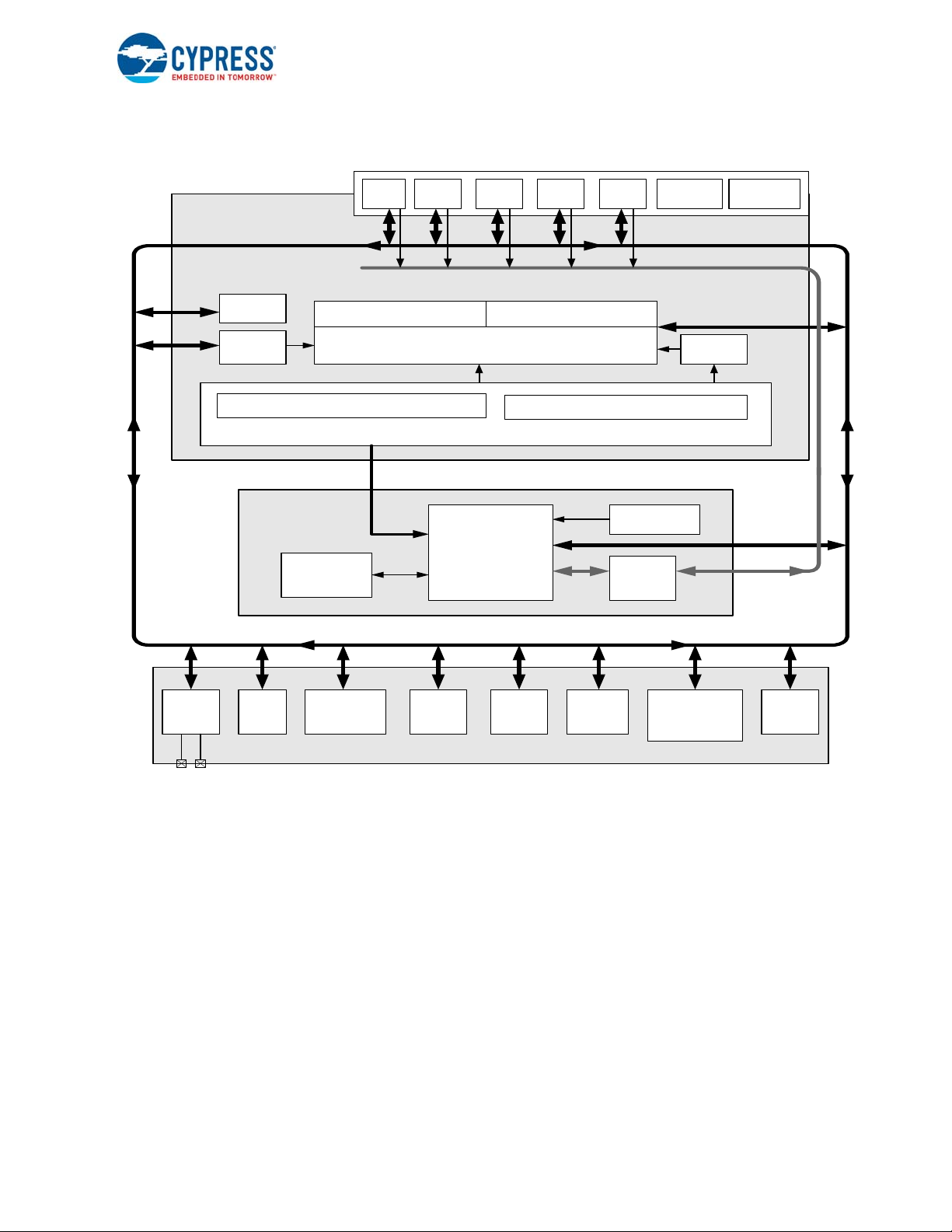
enCoRe V Core Top-Level Block Diagram
CAPSENSE
SYSTEM
1K/2K
SRAM
Inte rrupt
Controller
Sleep and
Watchdog
M ultip le Clo ck Sou rce s
Inte rna l Lo w Sp ee d O sc illator (IL O )
6/1 2/24 M H z In terna l M ain O sc illato r
(IM O)
PSoC CORE
CPU Core (M8C)
Supervisory ROM (SROM )
8K/16K/32K Flash
Nonvolatile M emory
SYSTEM RESOURCES
SYSTEM BUS
Analog
Reference
SYSTEM BUS
Port 3 Port 2 Port 1 P or t 0
CapSense
Module
Global Analog Interconnect
1.8/2.5/3V
LDO
Analog
Mux
Two
Com parators
I2C
Slave
SPI
Master/
Slave
POR
and
LVD
USB
System
Resets
Internal
Voltage
References
Three 16-Bit
Program mable
Tim ers
PWRSYS
(Regulator)
Port 4
Digital
Clocks
enCoRe™ V CY7C643xx, enCoRe™ V LV CY7C604xx TRM, Document No. 001-32519 Rev *H 11
Page 12

Getting Started
The quickest path to understanding enCoRe V is by reading the enCoRe V device’s datasheet and using PSoC Designer™
Integrated Development Environment (IDE). This manual is useful for understanding the details of the enCoRe V integrated
circuit.
Important Note
For the most up-to-date Ordering, Packaging, or Electrical Specification information, refer to the individual
enCoRe V device’s datasheet or go to http://www.cypress.com.
Support
Free support for enCoRe V products is available online at http://www.cypress.com. Resources include Training Seminars,
Discussion Forums, Application Notes, TightLink Technical Support Email/Knowledge Base, and Application Support Technicians.
Technical Support can be reached at http://www.cypress.com/support.
Product Upgrades
Cypress provides scheduled upgrades and version enhancements for PSoC Designer free of charge. You can order the
upgrades from your distributor on CD-ROM or download them directly from http://www.cypress.com under Software. Also pro-
vided are critical updates to system documentation under http://www.cypress.com >> Documentation.
Development Kits
Development Kits are available from the following distributors: Digi-Key, Avnet, Arrow, and Future. The Cypress Online Store
contains development kits, C compilers, and all accessories for enCoRe V development. Go to the Cypress Online Store at
http://www.cypress.com under Order >> USB Kits.
Document History
This section serves as a chronicle of the CY8C20XX6A/AS/LenCoRe™ V and enCoRe™ V LV CY7C643xx and CY7C604xx
Technical Reference Manual.
Technical Reference Manual History
Versio n/
Release Date
** September 2007 HMT First release of the enCoRe™ V and enCoRe™ V LV CY7C643xx and CY7C604xx Technical Reference Manual.
*A June 2008 HMT Second release of the enCoRe™ V and enCoRe™ V LV CY7C643xx and CY7C604xx Technical Reference Manual.
*B June 2009 FSU Third release of the enCoRe™ V and enCoRe™ V LV CY7C643xx and CY7C604xx Technical Reference Manual.
*C September 2009 FSU Fourth release of the enCoRe™ V and enCoRe™ V LV CY7C643xx and CY7C604xx Technical Reference Manual.
*D November 2009 FSU Multiple fixes, primarily to the sleep and I2C chapters.
*E December 2009 FSU Multiple fixes, primarily to the External Crystal Oscillator chapter.
*F September 2012 ANTG Updated external clock source description
*G October 2015 ASRI
*H November 2018 RAJV Updated the template
Originator Description of Change
Removed all instances of IMODIS related information and provided information for "no glitch protection in the device for
an external clock".
enCoRe™ V CY7C643xx, enCoRe™ V LV CY7C604xx TRM, Document No. 001-32519 Rev *H 12
Page 13
Documentation Conventions
There are only four distinguishing font types used in this
manual, besides those found in the headings.
■ The first is the use of italics when referencing a docu-
ment title or file name.
■ The second is the use of bold italics when referencing a
term described in the Glossary of this manual.
■ The third is the use of Times New Roman font, distinguish-
ing equation examples.
■ The fourth is the use of Courier New font, distinguish-
ing code examples.
Register Conventions
The following table lists the register conventions that are
specific to this manual. A more detailed set of register conventions is located in the Register Reference chapter on
page 163.
Register Conventions
Convention Example Description
‘x’ in a register
name
R R : 00 Read register or bit(s)
W W : 00 Write register or bit(s)
O RO : 00 Only a read/write register or bit(s).
L RL : 00 Logical register or bit(s)
C RC : 00 Clearable register or bit(s)
00 RW : 00 Reset value is 0x00 or 00h
XX RW : XX Register is not reset
0, 0,04h Register is in bank 0
1, 1,23h Register is in bank 1
x, x,F7h
Empty, grayedout table cell
PRTxIE
Multiple instances/address ranges of the
same register
Register exists in register bank 0 and register bank 1
Reserved bit or group of bits, unless otherwise stated
Numeric Naming
Hexadecimal numbers are represented with all letters in
uppercase with an appended lowercase ‘h’ (for example,
‘14h’ or ‘3Ah’) and hexadecimal numbers may also be represented by a ‘0x’ prefix, the C coding convention. Binary
numbers have an appended lowercase ‘b’ (for example,
01010100b’ or ‘01000011b’). Numbers not indicated by an
‘h’ or ‘b’ are decimal.
Units of Measure
This table lists the units of measure used in this manual.
Units of Measure
Symbol Unit of Measure
°C degrees Celsius
dB decibels
fF femtofarads
Hz hertz
k kilo, 1000
K
KB 1024 bytes
Kbit 1024 bits
kHz kilohertz (32.000)
k kilohms
MHz megahertz
M megaohms
A microamperes
F microfarads
s microseconds
V microvolts
Vrms microvolts root-mean-square
mA milliamperes
ms milliseconds
mV millivolts
nA nanoampheres
ns nanoseconds
nV nanovolts
ohms
pF picofarads
pp peak-to-peak
ppm parts per million
sps samples per second
sigma: one standard deviation
V volts
210, 1024
enCoRe™ V CY7C643xx, enCoRe™ V LV CY7C604xx TRM, Document No. 001-32519 Rev *H 13
Page 14
Acronyms
This table lists the acronyms that are used in this manual.
Acronyms
Acronym Description
ABUS analog output bus
AC alternating current
ADC analog-to-digital converter
API Application Programming Interface
BR bit rate
BRA bus request acknowledge
BRQ bus request
CI carry in
CMP compare
CO carry out
CPU central processing unit
CRC cyclic redundancy check
DAC digital-to-analog converter
DC direct current
DI digital or data input
DMA direct memory access
DO digital or data output
ECO external crystal oscillator
FB feedback
GIE global interrupt enable
GPIO general-purpose I/O
ICE in-circuit emulator
IDE integrated development environment
ILO internal low-speed oscillator
IMO internal main oscillator
I/O input/output
IOR I/O read
IOW I/O write
IPOR imprecise power-on-reset
IRQ interrupt request
ISR interrupt service routine
ISSP in system serial programming
IVR interrupt vector read
LRb last received bit
LRB last received byte
LSb least significant bit
LSB least significant byte
MISO master-in-slave-out
MOSI master-out-slave-in
MSb most significant bit
MSB most significant byte
PC program counter
PCH program counter high
PCL program counter low
PD power down
PMA PSoC® memory arbiter
POR power-on-reset
Acronyms (continued)
Acronym Description
PPOR precision power-on-reset
PRS pseudo random sequence
PSSDC power system sleep duty cycle
RAM random access memory
RETI return from interrupt
RO relaxation oscillator
ROM read-only memory
RW read/write
SIE serial interface engine
SE0 single-ended zero
SOF start of frame
SP stack pointer
SPI serial peripheral interconnect
SPIM serial peripheral interconnect master
SPIS serial peripheral interconnect slave
SRAM static random access memory
SROM supervisory read-only memory
SSADC single slope ADC
SSC supervisory system call
TC terminal count
USB universal serial bus
WDT watchdog timer
WDR watchdog reset
XRES external reset
enCoRe™ V CY7C643xx, enCoRe™ V LV CY7C604xx TRM, Document No. 001-32519 Rev *H 14
Page 15
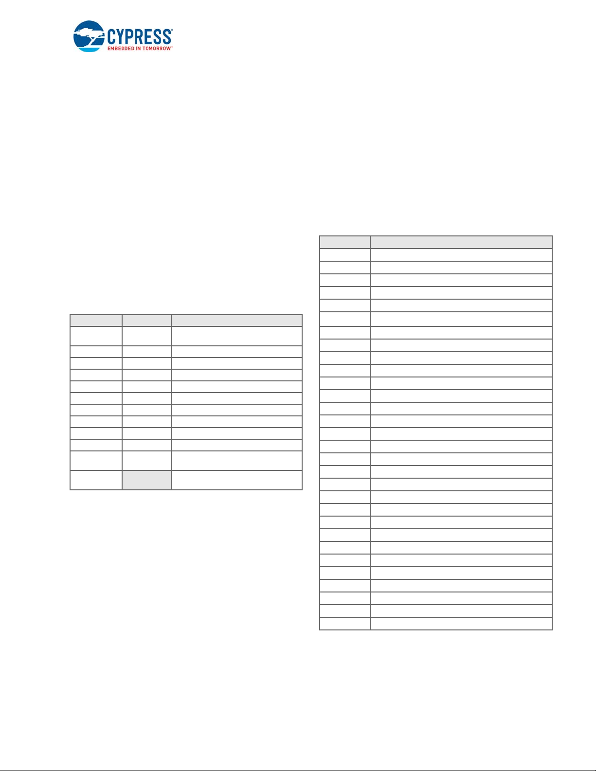
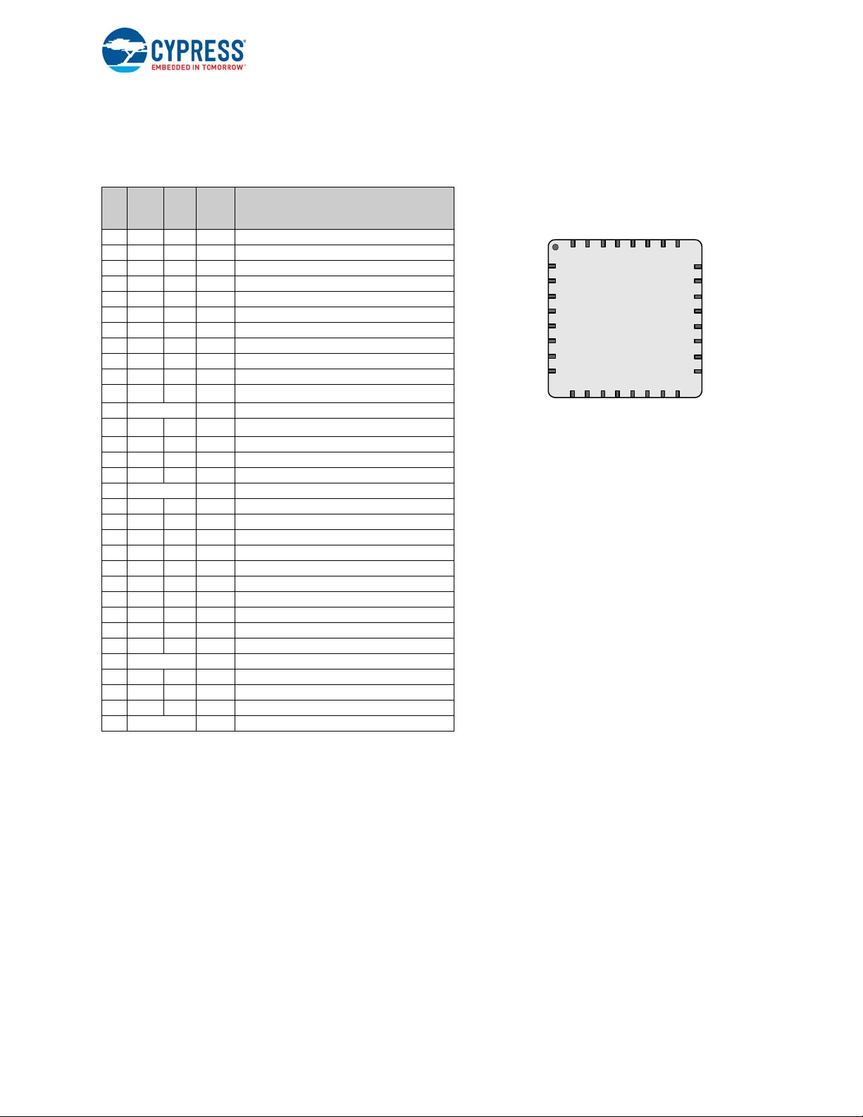
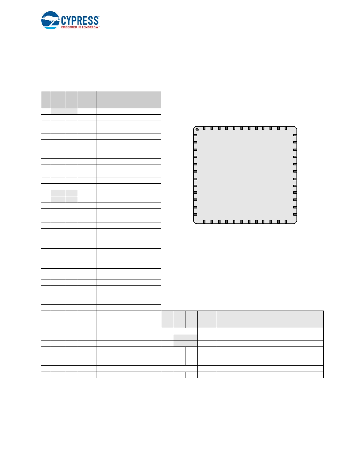
1. Pin Information
P2[5]
P1[7]
P1[5]
P1[3]
P0[3]
P0[7]
Vdd
P0[4]
P1[1]
P1[0]
P1[2]
P2[3]
P1[4]
XRES
P0[1]
Vss
QFN
(Top View)
1
2
3
4
12
11
10
9
161514
13
567
8
This chapter lists, describes, and illustrates all pins and pinout configurations for the CY8C20X46A/46AS/96A/46L/
96LCY7C643xx and CY7C604xx enCoRe V devices. For up-to-date ordering, pinout, and packaging information, refer to the
individual enCoRe V device’s datasheet or go to http://www.cypress.com.
1.1 Pinouts
TheCY8C20X46A/46AS/96A/46L/96LCY7C643xx and CY7C604xx enCoRe V devices are available in a variety of packages.
Every port pin (labeled with a “P”), except for Vss, Vdd, and XRES in the following tables and illustrations, is capable of Dig-
ital I/O.
1.1.1 CY7C60413 enCoRe V LV 16-Pin Part Pinout
Table 1-1. 16-Pin QFN/COL Part Pinout
Pin
No.
1 IO I P2[5] XTAL Out
2 IO I P2[3] XTAL In
3 IOHR I P1[7] I2C SCL, SPI SS
4 IOHR I P1[5] I2C SDA, SPI MISO
5 IOHR I P1[3] SPI CLK
6 IOHR I P1[1]
7 Power Vss Ground pin
8 IOHR I P1[0]
9 IOHR I P1[2]
10 IOHR I P1[4] EXTCLK
11 Input XRES Active high external reset with internal pull down
12 IOH I P0[4]
13 Power Vdd Power pin
14 IOH I P0[7]
15 IOH I P0[3]
16 IOH I P0[1]
Legend A = Analog, I = Input, O = Output, H = 5-mA High Output Drive, R = Regulated Output Option.
Typ e
Digital Analog
1
These are the ISSP pins, which are not High-Z at POR.
Name Description
1
TC CLK
, I2C SCL, SPI MOSI
1
TC DATA
, I2C SDA, SPI CLK
Devices
,
enCoRe™ V CY7C643xx, enCoRe™ V LV CY7C604xx TRM, Document No. 001-32519 Rev *H 15
Page 16
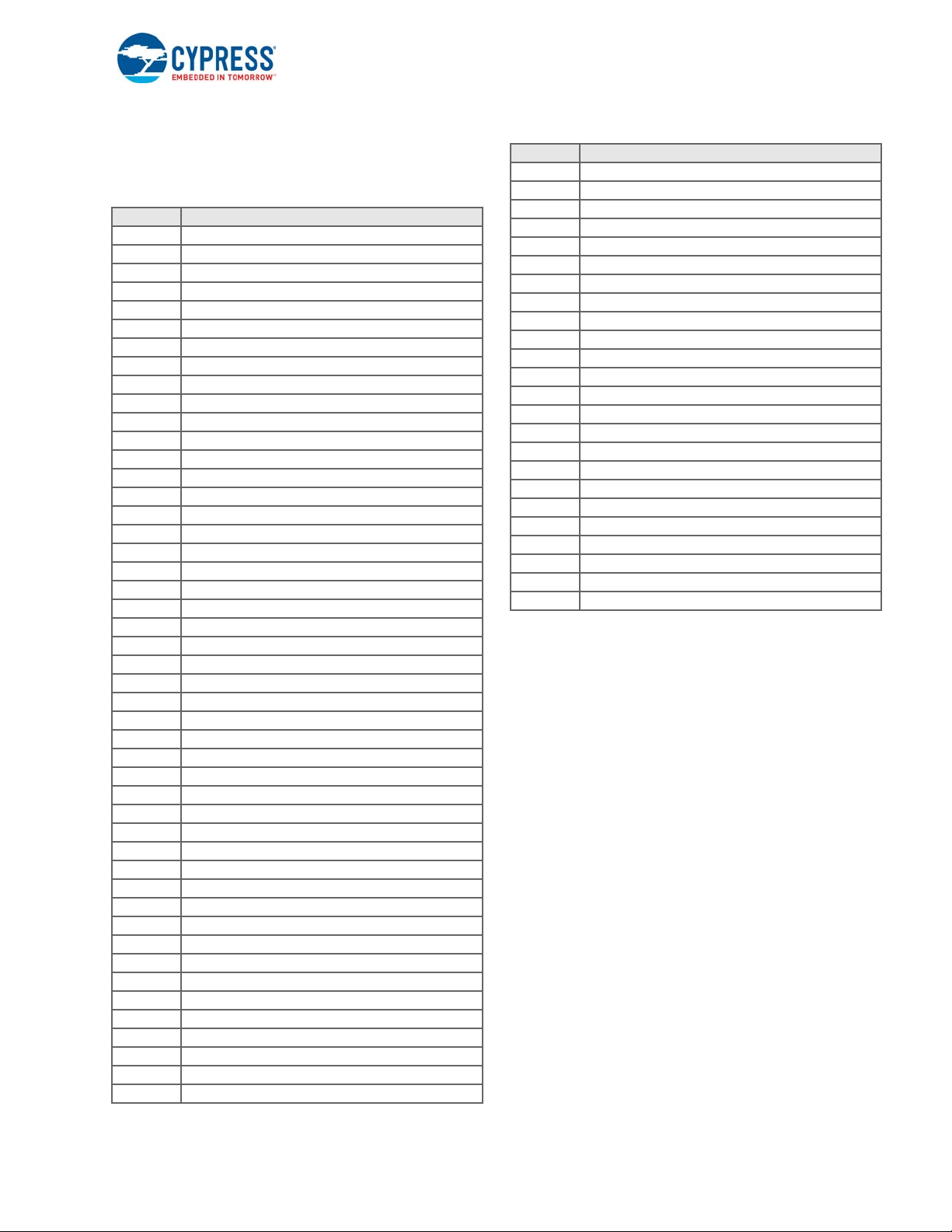
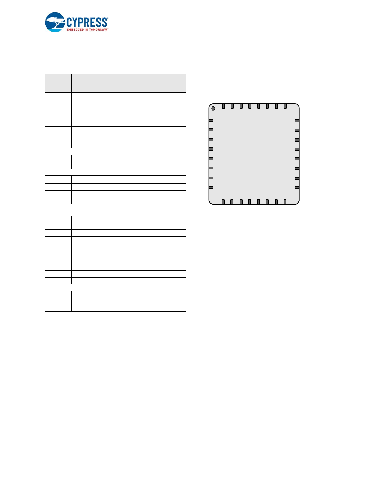
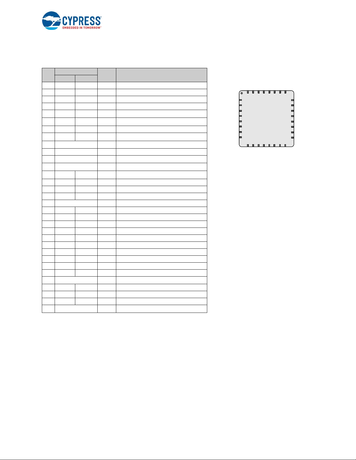
1.1.2
P0[1]
P2[7]
P2[5]
P2[3]
P2[1]
P3[3]
QFN
(Top View)
9
101112
131415
16
1
2
3
4
5
6
7
8
24
23
22
21
20
19
18
17
32313029282726
25
Vss
P0[3]
P0[7]
Vdd
P0[6]
P0[4]
P0[2]
P3[1]
P1[7]
P0[0]
P2[6]
P3[0]
XRES
P1[5]
P1[3]
P1[1]
Vss
P1[0]
P1[2]
P1[4]
P1[6]
P2[4]
P2[2]
P2[0]
P3[2]
P0[5]
Pin Information
CY7C60445 enCoRe V LV 32-Pin Part Pinout
Table 1-2. 32-Pin QFN Part Pinout
Pin
No.
Digital
1 IOH I P0[1] Integrating input
2 IO I P2[7]
3 IO I P2[5] XTAL Out
4 IO I P2[3] XTAL In
5 IO I P2[1]
6 IO I P3[3]
7 IO I P3[1]
8 IOHR I P1[7] I2C SCL, SPI SS
9 IOHR I P1[5] I2C SDA, SPI MISO
10 IOHR I P1[3] SPI CLK
11 IOHR I P1[1]
12 Power Vss Ground pin
13 IOHR I P1[0]
14 IOHR I P1[2]
15 IOHR I P1[4] EXTCLK
16 IOHR I P1[6]
17 Input XRES Active high external reset with internal pull down
18 IO I P3[0]
19 IO I P3[2]
20 IO I P2[0]
21 IO I P2[2]
22 IO I P2[4]
23 IO I P2[6]
24 IOH I P0[0]
25 IOH I P0[2]
26 IOH I P0[4]
27 IOH I P0[6]
28 Power Vdd Power pin
29 IOH I P0[7]
30 IOH I P0[5]
31 IOH I P0[3]
32 Power Vss Ground pin
Legend A = Analog, I = Input, O = Output, NC = No Connection, H = 5 mA High Output Drive, R = Regulated Output Option.
1
2
Name Description
Analog
TC CLK
TC DATA
These are the ISSP pins, which are not High-Z at POR.
The center pad on the QFN package must be connected to ground (Vss) for best mechanical, thermal, and electrical performance. If not connected to ground, it must be electrically floated and not connected to any other signal.
2
1
, I2C SCL, SPI MOSI
1
, I2C SDA, SPI CLK
CY7C60445 enCoRe V LV Devices
enCoRe™ V CY7C643xx, enCoRe™ V LV CY7C604xx TRM, Document No. 001-32519 Rev *H 16
Page 17
1.1.3 CY7C64345, CY7C64343, enCoRe V 32-Pin Part Pinout
P0[1]
P2[5]
P2[3]
P2[1]
P1[7]
P1[5]
QFN
(Top View)
9
101112
131415
16
1
2
3
4
5
6
7
8
24
23
22
21
20
19
18
17
32313029282726
25
Vss
P0[3]
P0[7]
Vdd
P0[6]
P0[4]
P0[2]
P1[3]
P1[1]
P0[0]
P2[6]
P3[0]
XRES
Vss
D+
D-
Vdd
P1[0]
P1[2]
P1[4]
P1[6]
P2[4]
P2[2]
P2[0]
P3[2]
P0[5]
Pin Information
Table 1-3. 32-Pin QFN Part Pinout
Pin
No.
Digital
1 IOH I P0[1]
2 IO I P2[5] XTAL Out
3 IO IP2[3]XTAL In
4 IO I P2[1]
5 IOHR I P1[7] I2C SCL, SPI SS
6 IOHR I P1[5] I2C SDA, SPI MISO
7 IOHR I P1[3] SPI CLK
8 IOHR I P1[1]
9 Power Vss Ground pin
10 IO D+ USB PHY
11 IO D- USB PHY
12 Power Vdd Power pin
13 IOHR I P1[0]
14 IOHR I P1[2]
15 IOHR I P1[4] EXTCLK
16 IOHR I P1[6]
17 Input XRES Active high external reset with internal
18 IO IP3[0]
19 IO IP3[2]
20 IO IP2[0]
21 IO I P2[2]
22 IO I P2[4]
23 IO I P2[6]
24 IOH I P0[0]
25 IOH I P0[2]
26 IOH I P0[4]
27 IOH I P0[6]
28 Power Vdd Power pin
29 IOH I P0[7]
30 IOH I P0[5]
31 IOH I P0[3]
32 Power Vss Ground pin
LEGEND A = Analog, I = Input, O = Output, NC = No Connection, H = 5 mA High Output Drive, R = Regulated Output Option.
1
2
Name Description
Analog
TC CLK
TC DATA
pull down
These are the ISSP pins, which are not High Z at POR (Power On Reset).
The center pad on the QFN package must be connected to ground (Vss) for best mechanical, thermal, and electrical performance. If not connected to ground, it must be electrically floated and not connected to any other signal.
2
1
, I2C SCL, SPI MOSI
1
, I2C SDA, SPI CLK
CY7C64345, CY7C64343 enCoRe V Devices
enCoRe™ V CY7C643xx, enCoRe™ V LV CY7C604xx TRM, Document No. 001-32519 Rev *H 17
Page 18
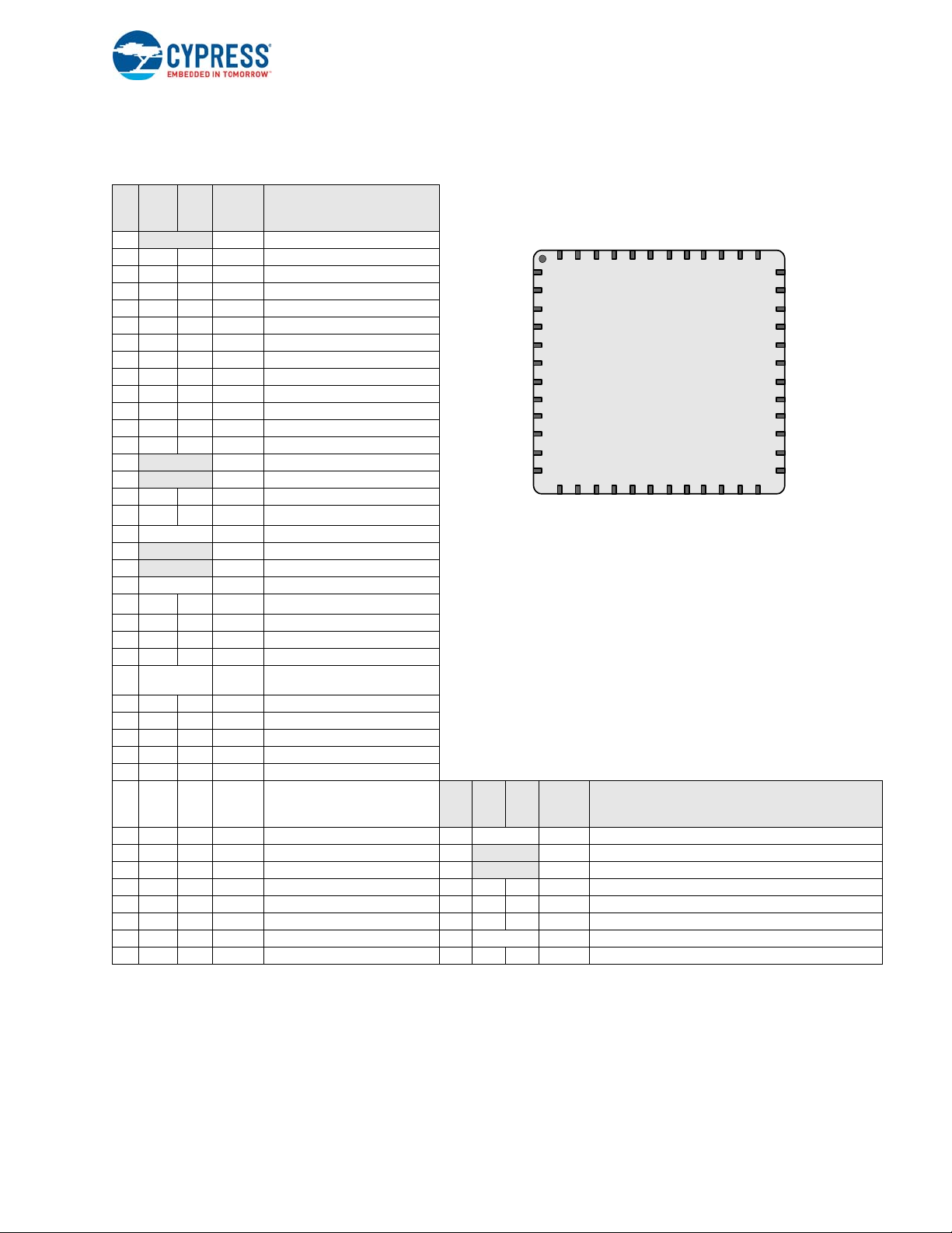
1.1.4 CY8C20646A/AS/LCY8C20666A/AS/L
QFN
(Top View)
P0[1]
Vss
P0[3]
P0[5]
P0[7]NCNC
Vdd
P0[6]
P0[4]
P0[2]
P0[0]
10
11
12
P2[7]
NC
P2[5]
P2[3]
P2[1]
P4[3]
P4[1]
P3[7]
P3[5]
P3[3]
P3[1]
P1[7]
35
34
33
32
31
30
29
28
27
26
25
36
4847464544
43424140393837
P2[4]
P2[2]
P2[0]
P4[2]
P4[0]
P3[6]
P3[4]
P3[2]
P3[0]
XRES
P1[6]
P2[6]
1
2
3
4
5
6
7
8
9
131415161718192021
22
23
24
P1[5]
NC
NC
P1[3]
P1[1]
Vss
D+
D-
Vdd
P1[0]
P1[2]
P1[4]
CY7C64355, CY7C64356 enCoRe V 48-Pin Part Pinout
Pin Information
TC CLK
TC DATA
2
1
, I2C SCL, SPI MOSI
1
, I2C SDA, SPI CLK
CY7C64355, CY7C64356 enCoRe VDevices
Pin
No.
Digital
Name Description31 IO I P4[0]
Analog
Table 1-4. 48-Pin Part Pinout
Pin
No.
Digital
1 NC No connection
2 IO I P2[7]
3 IO I P2[5] XTAL Out
4 IO I P2[3] XTAL In
5 IO I P2[1]
6 IO I P4[3]
7 IO IP4[1]
8 IO I P3[7]
9 IO I P3[5]
10 IO I P3[3]
11 IO I P3[1]
12 IOHR I P1[7] I2C SCL, SPI SS
13 IOHR I P1[5] I2C SDA, SPI MISO
14 NC No connection
15 NC No connection
16 IOHR I P1[3] SPI CLK
17 IOHR I P1[1]
18 Power Vss Ground pin
19 IO D + USB PHY
20 IO D - USB PHY
21 Power Vdd Power pin
22 IOHR I P1[0]
23 IOHR I P1[2]
24 IOHR I P1[4] EXTCLK
25 IOHR I P1[6]
26 Input XRES Active high external reset with internal pull down
27 IO I P3[0]
28 IO IP3[2]
29 IO IP3[4]
30 IO IP3[6]
32 IO I P4[2]
33 IO I P2[0] 41 Power Vdd Power pin
34 IO I P2[2] 42 NC No connection
35 IO I P2[4] 43 NC No connection
36 IO I P2[6] 44 IOH I P0[7]
37 IOH I P0[0] 45 IOH I P0[5]
38 IOH I P0[2] 46 IOH I P0[3]
39 IOH I P0[4] 47 Power Vss Ground pin
40 IOH I P0[6] 48 IOH I P0[1]
Legend A = Analog, I = Input, O = Output, NC = No Connection, H = 5 mA High Output Drive, R = Regulated Output Option.
1
2
Name Description
Analog
These are the ISSP pins, which are not High-Z at POR.
The center pad on the QFN package must be connected to ground (Vss) for best mechanical, thermal, and electrical performance. If not connected
to ground, it must be electrically floated and not connected to any other signal.
enCoRe™ V CY7C643xx, enCoRe™ V LV CY7C604xx TRM, Document No. 001-32519 Rev *H 18
Page 19
1.1.5 CY7C60455, CY7C60456 enCoRe V LV 48-Pin Part Pinout
QFN
(Top View)
P0[1]
Vss
P0[3]
P0[5]
P0[7]NCNC
Vdd
P0[6]
P0[4]
P0[2]
P0[0]
10
11
12
P2[7]
NC
P2[5]
P2[3]
P2[1]
P4[3]
P4[1]
P3[7]
P3[5]
P3[3]
P3[1]
P1[7]
35
34
33
32
31
30
29
28
27
26
25
36
4847464544
43424140393837
P2[4]
P2[2]
P2[0]
P4[2]
P4[0]
P3[6]
P3[4]
P3[2]
P3[0]
XRES
P1[6]
P2[6]
1
2
3
4
5
6
7
8
9
131415161718192021
22
23
24
P1[5]
NC
NC
P1[3]
P1[1]
Vss
NC
NC
Vdd
P1[0]
P1[2]
P1[4]
Pin Information
Table 1-5. 48-Pin Part Pinout
Pin
No.
Digital
1 NC No connection
2 IO I P2[7]
3 IO I P2[5] XTAL Out
4 IO I P2[3] XTAL In
5 IO I P2[1]
6 IO I P4[3]
7 IO IP4[1]
8 IO I P3[7]
9 IO I P3[5]
10 IO I P3[3]
11 IO I P3[1]
12 IOHR I P1[7] I2C SCL, SPI SS
13 IOHR I P1[5] I2C SDA, SPI MISO
14 NC No connection
15 NC No connection
16 IOHR I P1[3] SPI CLK
17 IOHR I P1[1]
18 Power Vss Ground pin
19 NC No connection
20 NC No connection
21 Power Vdd Power pin
22 IOHR I P1[0]
23 IOHR I P1[2]
24 IOHR I P1[4] EXTCLK
25 IOHR I P1[6]
26 Input XRES Active high external reset with
27 IO I P3[0]
28 IO IP3[2]
29 IO IP3[4]
30 IO IP3[6]
31 IO I P4[0]
32 IO I P4[2]
33 IO I P2[0] 41 Power Vdd Power pin
34 IO I P2[2] 42 NC No connection
35 IO I P2[4] 43 NC No connection
36 IO I P2[6] 44 IOH I P0[7]
37 IOH I P0[0] 45 IOH I P0[5]
38 IOH I P0[2] 46 IOH I P0[3]
39 IOH I P0[4] 47 Power Vss Ground pin
40 IOH I P0[6] 48 IOH I P0[1]
LEGEND
A = Analog, I = Input, O = Output, NC = No Connection, H = 5 mA High Output Drive, R = Regulated Output Option.
1
2
enCoRe™ V CY7C643xx, enCoRe™ V LV CY7C604xx TRM, Document No. 001-32519 Rev *H 19
2
CY7C60455, CY7C60456 enCoRe V LV Devices
Name Description
Analog
1
TC CLK
, I2C SCL, SPI MOSI
1
TC DATA
internal pull down
These are the ISSP pins, which are not High Z at POR (Power On Reset).
The center pad on the QFN package must be connected to ground (Vss) for best mechanical, thermal, and electrical performance. If not connected to ground, it must be electrically floated and not connected to any other signal.
, I2C SDA, SPI CLK
Pin
No.
Digital
Name Description
Analog
Page 20
Pin Information
QFN
(Top View)
P0[1]
Vss
P0[3]
P0[5]
P0[7]
OCDE
OCDO
Vdd
P0[6]
P0[4]
P0[2]
P0[0]
10
11
12
P2[7]
OCDOE
P2[5]
P2[3]
P2[1]
P4[3]
P4[1]
P3[7]
P3[5]
P3[3]
P3[1]
P1[7]
35
34
33
32
31
30
29
28
27
26
25
36
4847464544
43424140393837
P2[4]
P2[2]
P2[0]
P4[2]
P4[0]
P3[6]
P3[4]
P3[2]
P3[0]
XRES
P1[6]
P2[6]
1
2
3
4
5
6
7
8
9
131415161718192021
22
23
24
P1[5]
CCLK
HCLK
P1[3]
P1[1]
Vss
D +
D -
Vdd
P1[0]
P1[2]
P1[4]
1.1.6 CY8C20066A, CY8CTMG200-00LTXI, CY8CTMG200A-00LTXI PSoC, CY7C64300 enCoRe V and CY7C60400 enCoRe V LV OCD 48-Pin Part Pinout
The 48-pin QFN part is for on-chip debugging (OCD). Note that this part is only used for in-circuit debugging. It is NOT avail-
able for production.
Table 1-6. 48-Pin OCD Part Pinout
Pin
No.
Digital
1 OCDOE OCD directional pin
2 IO I P2[7]
3 IO I P2[5] XTAL Out
4 IO I P2[3] XTAL In
5 IO I P2[1]
6 IO I P4[3]
7 IO IP4[1]
8 IO I P3[7]
9 IO I P3[5]
10 IO I P3[3]
11 IO I P3[1]
12 IOHR I P1[7] I2C SCL, SPI SS
13 IOHR I P1[5] I2C SDA, SPI MISO
14 CCLK OCD CPU CLK OUTPUT
15 HCLK OCD HIGH SPEED CLK
16 IOHR I P1[3] SPI CLK
17 IOHR I P1[1]
18 Power Vss Ground pin
19 IO D+ USB PHY
20 IO D– USB PHY
21 Power Vdd Power pin
22 IOHR I P1[0]
23 IOHR I P1[2]
24 IOHR I P1[4] EXTCLK
25 IOHR I P1[6]
26 Input XRES Active high external reset with
27 IO I P3[0]
28 IO IP3[2]
29 IO IP3[4]
30 IO IP3[6]
31 IO I P4[0]
32 IO I P4[2]
33 IO I P2[0] 41 Power Vdd Power pin
34 IO I P2[2] 42 OCDO OCD even data I/O
35 IO I P2[4] 43 OCDE OCD odd data output
36 IO I P2[6] 44 IOH I P0[7]
37 IOH I P0[0] 45 IOH I P0[5]
38 IOH I P0[2] 46 IOH I P0[3]
39 IOH I P0[4] 47 Power Vss Ground pin
40 IOH I P0[6] 48 IOH I P0[1]
Legend
A = Analog, I = Input, O = Output, NC = No Connection, H = 5-mA High Output Drive, R = Regulated Output Option.
1
2
Name Description
Analog
TC CLK
TC DATA
internal pull down
ISSP pin which is not High-Z at POR.
The center pad (CP) on the QFN package must be connected to ground (VSS) for best mechanical, thermal, and electrical performance. If not connected to ground, it must be electrically floated and not connected to any other signal.
enCoRe™ V CY7C643xx, enCoRe™ V LV CY7C604xx TRM, Document No. 001-32519 Rev *H 20
2
1
, I2C SCL, SPI MOSI
1
, I2C SDA, SPI CLK
CY8C20066A, CY8CTMG200-00LTXI, CY8CTMG200A-00LTXI,
CY7C64300, CY7C60400 enCoRe V OCD Devices
NOT FOR PRODUCTION – OCD Part
Pin
No.
Digital
Name Description
Analog
Page 21
1.1.7 32-Pin QFN (with USB)
P0[1]
P2[5]
P2[3]
P2[1]
P1[7]
P1[5]
QFN
(Top View)
9
101112
131415
16
1
2
3
4
5
6
7
8
24
23
22
21
20
19
18
17
32313029282726
25
Vss
P0[3]
P0[7]
Vdd
P0[6]
P0[4]
P0[2]
P1[3]
P1[1]
P0[0]
P2[6]
P3[0]
XRES
Vss
USB PHY, D+
USB D–
Vdd
P1[0]
P1[2]
P1[4]
P1[6]
P2[4]
P2[2]
P2[0]
P3[2]
P0[5]
Pin Information
Table 1-7. Pin Definitions – CY8C20496A/L PSoC Device
Pin
No.
Typ e
Digital Analog
Name Description
2
1 IOH I P0[1] Integrating Input
2 I/O I P2[5] XTAL Out
3 I/O I P2[3] XTAL In
4 I/O I P2[1]
5 IOHR I P1[7]
6 IOHR I P1[5]
2
I
C SCL, SPI SS
2
I
C SDA, SPI MISO
7 IOHR I P1[3] SPI CLK
8 IOHR I P1[1]
9 Power V
SS
ISSP CLK
Ground Pin
1
, I2C SCL, SPI MOSI
10 I D+ USB D+
11
I
12 Power V
13 IOHR I P1[0]
D– USB D–
Power pin
DD
ISSP DATA
1
, I2C SDA, SPI CLKI
3
14 IOHR I P1[2]
15 IOHR I P1[4] Optional external clock input (EXTCLK)
16 IOHR I P1[6]
17 Input XRES Active high external reset with internal pull-down
18 I/O I P3[0]
19 I/O I P3[2]
20 I/O I P2[0]
21 I/O I P2[2]
22 I/O I P2[4]
23 I/O I P2[6]
24 IOH I P0[0]
25 IOH I P0[2]
26 IOH I P0[4]
27 IOH I P0[6]
28 Power V
DD
Power Pin
29 IOH I P0[7]
30 IOH I P0[5]
31 IOH I P0[3] Integrating Input
32 Power V
A = Analog, I = Input, O = Output, OH = 5 mA High Output Drive, R = Regulated Output.
Legend
1
On power-up, the SDA(P1[0]) drives a strong high for 256 sleep clock cycles and drives resistive low for the next 256 sleep clock cycles. The
SCL(P1[1])line drives resistive low for 512 sleep clock cycles and both the pins transition to high-impedance state. On reset, after XRES deasserts, the SDA and the SCL lines drive resistive low for 8 sleep clock cycles and transition to high-impedance state. Hence, during power-up or
reset event, P1[1] and P1[0] may disturb the I2C bus. Use alternate pins if you encounter issues.
2
The center pad on the QFN package must be connected to ground (Vss) for best mechanical, thermal, and electrical performance. If not con-
nected to ground, it must be electrically floated and not connected to any other signal.
3
Alternate SPI clock.
Ground Pin
SS
CY8C20496A/L PSoC Device
enCoRe™ V CY7C643xx, enCoRe™ V LV CY7C604xx TRM, Document No. 001-32519 Rev *H 21
Page 22
1.1.8 48-Pin SSOP
P0[7]
Vdd
P0[5]
P0[6]
P0[3]
P0[4]
0[1] P0[2]
P2[7]
P0[0]
P2[5]
P2[6]
P2[3]
P2[4]
P2[1]
P2[2]
NC
P2[0]
NC
P3[6]
P4[3]
P3[4]
P4[1]
P3[2]
NC
P3[0]
P3[7]
XRES
P3[5]
NC
P3[3]
NC
P3[1] NC
NC
NC
NC
NC
P1[7]
NC
P1[5 ]
P1[6]
P1[3]
P1[4]
P1[1] P1[2]
Vss P1[0]
P
SSOP
1
2
3
4
5
6
7
8
9
10
11
12
13
14
15
16
17
18
19
20
21
22
23
24
48
47
46
45
43
44
42
40
41
39
38
37
36
35
33
34
32
31
30
29
28
27
26
25
Table 1-8. Pin Definitions – CY8C20536A, CY8C20546A, and CY8C20566A PSoC Device
CY8C20536A, CY8C20546A, and CY8C20566A
PSoC Device
Digital
Pin No.
1 IOH I P0[7]
2 IOH I P0[5]
3 IOH I P0[3] Integrating Input
4 IOH I P0[1] Integrating Input
5 I/O I P2[7]
6 I/O I P2[5] XTAL Out
7 I/O IP2[3]XTAL In
8 I/O I P2[1]
9 NC No connection
10 NC No connection
11 I/O I P4[3]
12 I/O I P4[1]
13 NC No connection
14 I/O I P3[7]
15 I/O I P3[5]
16 I/O I P3[3]
17 I/O I P3[1]
18 NC No connection
19 NC No connection
20 IOHR I P1[7]
21 IOHR I P1[5]
22 IOHR I P1[3] SPI CLK
23 IOHR I P1[1]
24 V
25 IOHR I P1[0]
26 IOHR I P1[2]
27 IOHR I P1[4]
28 IOHR IP1[6]
29 NC No connection
30 NC No connection
31 NC No connection
32 NC No connection
Name
Analog
2
I
C SCL, SPI SS
2
I
C SDA, SPI MISO
ISSP CLK
Ground Pin
SS
ISSP DATA
1
, I2C SCL, SPI MOSI
1
Description
, I2C SDA, SPI CLK
2
Optional external clock input
(
EXT CLK)
Pin Information
33 NC No connection 41 I/O I P2[2]
34 NC No connection 42 I/O I P2[4]
35 XRES Active high external reset with internal
36 I/O I P3[0] 44 IOH I P0[0]
37 I/O I P3[2] 45 IOH I P0[2]
38 I/O I P3[4] 46 IOH I P0[4]
39 I/O I P3[6] 47 IOH I P0[6]
40 I/O I P2[0] 48 Power V
Legend A = Analog, I = Input, O = Output, NC = No Connection, H = 5 mA High Output Drive, R = Regulated Output Option.
enCoRe™ V CY7C643xx, enCoRe™ V LV CY7C604xx TRM, Document No. 001-32519 Rev *H 22
1
2
Analog
DD
Name
Description
Power Pin
Digital
Pin No.
pull-down
On power-up, the SDA(P1[0]) drives a strong high for 256 sleep clock cycles and drives resistive low for the next 256 sleep clock cycles. The
SCL(P1[1])line drives resistive low for 512 sleep clock cycles and both the pins transition to high-impedance state. On reset, after XRES deasserts, the SDA and the SCL lines drive resistive low for 8 sleep clock cycles and transition to high-impedance state. Hence, during power-up or
reset event, P1[1] and P1[0] may disturb the I2C bus. Use alternate pins if you encounter issues.
Alternate SPI clock.
43 I/O I P2[6]
Page 23
Section B: enCoRe V Core
1K, 2K
SRAM
Interrupt
Controller
Sleep and
Watchdog
Multiple Clock Sources
Internal Low Speed Oscillator (ILO)
6/12/24 MHz Internal Main Oscillator (IMO)
CORE
CPU Core (M8C)
Supervisory ROM (SROM)
8K, 16K, 32K Flash
Nonvolatile Memory
SYSTEM BUS
Port 3 Port 2 Port 1 Port 0
1.8/2.5/3V
LDO
PWRSYS
(Regulator)
Port 4
The enCoRe V Core section discusses the core components of an enCoRe V device with a base part number of CY7C643xx
and CY7C604xx and the registers associated with those components. The core section covers the heart of the enCoRe V
device, which includes the M8C microcontroller; SROM, interrupt controller, GPIO, and SRAM paging; multiple clock
sources such as IMO and ILO; and sleep and watchdog functionality. This section includes these chapters:
■ CPU Core (M8C) on page 26.
■ Supervisory ROM (SROM) on page 32.
■ RAM Paging on page 38.
■ Interrupt Controller on page 44.
■ General-Purpose I/O (GPIO) on page 52.
Top-Level Core Architecture
This figure displays the top-level architecture of the enCoRe V core. Each component of the figure is discussed at length in
this section.
enCoRe V Core Block Diagram
■ Internal Main Oscillator (IMO) on page 67.
■ Internal Low-speed Oscillator (ILO) on page 72.
■ External Crystal Oscillator (ECO), on page 74
■ Sleep and Watchdog on page 78.
enCoRe™ V CY7C643xx, enCoRe™ V LV CY7C604xx TRM, Document No. 001-32519 Rev *H 23
Page 24
Core Register Summary
This table lists all the enCoRe V registers for the CPU core in address order within their system resource configuration. The
grayed out bits are reserved bits. If you write these bits, always write them with a value of ‘0’. For the core registers, the first
‘x’ in some register addresses represents either bank 0 or bank 1. These registers are listed throughout this manual in bank
0, even though they are also available in bank 1.
Summary Table of the Core Registers
Address Name Bit 7 Bit 6 Bit 5 Bit 4 Bit 3 Bit 2 Bit 1 Bit 0 Access
M8C REGISTER
x,F7h CPU_F
x,6Ch TMP_DR0
x,6Dh TMP_DR1
x,6Eh TMP_DR2
x,6Fh TMP_DR3
0,D0h CUR_PP
0,D1h STK_PP
0,D3h IDX_PP
0,D4h MVR_PP
0,D5h MVW_PP
0,DAh INT_CLR0
0,DBh INT_CLR1
0,DCh INT_CLR2
0,DEh INT_MSK2
0,DFh INT_MSK1
0,E0h INT_MSK0
0,E1h INT_SW_EN
0,E2h INT_VC Pending Interrupt[7:0] RC : 00
0,00h PRT0DR Data[7:0] RW : 00
0,01h PRT0IE Interrupt Enables[7:0] RW : 00
0,04h PRT1DR Data[7:0] RW : 00
0,05h PRT1IE Interrupt Enables[7:0] RW : 00
0,08h PRT2DR Data[7:0] RW : 00
0,09h PRT2IE Interrupt Enables[7:0] RW : 00
0,0Ch PRT3DR Data[7:0] RW : 00
0,0Dh PRT3IE Interrupt Enables[7:0] RW : 00
1,00h PRT0DM0 Drive Mode 0[7:0] RW : 00
1,01h PRT0DM1 Drive Mode 1[7:0] RW : FF
1,04h PRT1DM0 Drive Mode 0[7:0] RW : 00
1,05h PRT1DM1 Drive Mode 1[7:0] RW : FF
1,08h PRT2DM0 Drive Mode 0[7:0] RW : 00
1,09h PRT2DM1 Drive Mode 1[7:0] RW : FF
1,0Ch PRT3DM0 Drive Mode 0[7:0] RW : 00
1,0Dh PRT3DM1 Drive Mode 1[7:0] RW : FF
0,10h PRTxDR Data[7:0] RW : 00
0,11h PRTxIE Interrupt Enables[7:0] RW : 00
1,10h PRTxDM0 Drive Mode 0[7:0] RW : 00
1,11h PRTxDM1 Drive Mode 0[7:0] RW : 00
PgMode[1:0] XIO_1 XIO Carry Zero GIE RL : 02
RAM PAGING (SRAM) REGISTERS (page 38)
INTERRUPT CONTROLLER REGISTERS (page 44)
I2C Sleep SPI GPIO Timer0 Reserved Reserved V Monitor RW : 00
Endpoint3 Endpoint2 Endpoint1 Endpoint0 USB SOF USB Bus Rst Timer2 Timer1 RW : 00
USB_WAKE Endpoint8 Endpoint7 Endpoint6 Endpoint5 Endpoint4 RW : 00
USB
Wakeu p
Endpoint3 Endpoint2 Endpoint1 Endpoint0 USB SOF
I2C Sleep SPI GPIO Timer0 Reserved Reserved V Monitor RW : 00
GENERAL-PURPOSE I/O (GPIO) REGISTERS (page 56)
(page 26)
Data[7:0] RW : 00
Data[7:0] RW : 00
Data[7:0] RW : 00
Data[7:0] RW : 00
Page Bits[2:0] RW : 0
Page Bits[2:0] RW : 0
Page Bits[2:0] RW : 0
Page Bits[2:0] RW : 0
Page Bits[2:0] RW : 0
Endpoint8 Endpoint7 Endpoint6 Endpoint5 Endpoint4 RW : 00
USB Bus
Reset
Timer2 Ti mer1 RW : 00
ENSWINT RW : 0
enCoRe™ V CY7C643xx, enCoRe™ V LV CY7C604xx TRM, Document No. 001-32519 Rev *H 24
Page 25
Summary Table of the Core Registers (continued)
Address Name Bit 7 Bit 6 Bit 5 Bit 4 Bit 3 Bit 2 Bit 1 Bit 0 Access
1,DCh IO_CFG1 StrongP Range[1:0]
INTERNAL MAIN OSCILLATOR (IMO) REGISTER (page 68)
1,E8h IMO_TR Trim[7:0] W: 00
1,FAh IMO_TR1
x,FEh CPU_SCR1
1,E2h OSC_CR2
1,E9h ILO_TR
1,D2h ECO_ENBUS
1,D3h ECO_TRIM
1,E1h ECO_CFG
0,E3h RES_WDT WDSL_Clear[7:0] W : 00
1,EBh SLP_CFG
1,ECh SLP_CFG2
1,EDh SLP_CFG3
Legend
L The and f, expr; or f, expr; and xor f, expr instructions can be used to modify this register.
x An “x” before the comma in the address field indicates that this register can be accessed or written to no matter what bank is used.
C Clearable register or bit(s).
R Read register or bit(s).
W Write register or bit(s).
IRESS SLIM[1:O] IRAMDIS # : 00
CLK48MEN EXTCLKEN RSVD RW : 00
INTERNAL LOW-SPEED OSCILLATOR (ILO) REGISTER (page 73)
PD_MODE ILOFREQ SATBIASB Freq Trim[3:0] RW : 18
EXTERNAL CRYSTAL OSCILLATOR (ECO) REGISTERS (page 74)
SLEEP AND WATCHDOG REGISTERS (page 82)
PSSDC[1:0] RW : 0
DBL_TAPS T2TAP [1:0] T1TAP [1:0] T0TAP [1:0] RW : 0x7F
P1_LOW_
THRS
ECO_XGM[2:0] ECO_LP[1:0] RW : 00
SPICLK_ON
_P10
ECO_LPM ECO_EXW ECO_EX RW : 00
ALT_Buzz [1:0] I2C_ON LSO_OFF RW : 00
REG_EN IOINT RW : 00
Fine Trim[2:0] RW : 00
ECO_ENBUS[2:0] RW : 07
enCoRe™ V CY7C643xx, enCoRe™ V LV CY7C604xx TRM, Document No. 001-32519 Rev *H 25
Page 26

2. CPU Core (M8C)
This chapter explains the CPU Core, called the M8C, and its associated register. It covers the internal M8C registers, address
spaces, instruction set and formats. For additional information concerning the M8C instruction set, refer to the PSoC
Designer Assembly Language User Guide available at http://www.cypress.com. For a quick reference of all enCoRe V regis-
ters in address order, refer to the Register Reference chapter on page 163.
2.1 Overview
The M8C is a four MIPS 8-bit Harvard architecture micropro-
cessor. Selectable processor clock speeds up to 24 MHz
enable you to tune the M8C to a particular application’s performance and power requirements. The M8C supports a rich
instruction set that allows for efficient low-level language
support.
2.2 Internal Registers
The M8C has five internal registers that are used in program
execution. Here is a list of these registers.
■ Accumulator (A)
■ Index (X)
■ Program Counter (PC)
■ Stack Pointer (SP)
■ Flags (F)
All the internal M8C registers are 8 bits in width, except for
the PC, which is 16 bits wide. Upon reset, A, X, PC, and SP
are reset to 00h. The Flag register (F) is reset to 02h, indi-
cating that the Z flag is set.
With each stack operation, the SP is automatically incre-
mented or decremented so that it always points to the next
stack byte in RAM. If the last byte in the stack is at address
, the stack pointer wraps to RAM address 00h. It is the
FFh
firmware developer’s responsibility to ensure that the stack
does not overlap with user-defined variables in RAM.
The F register is read by using address F7h in either register
bank.
2.3 Address Spaces
The M8C has three address spaces: ROM, RAM, and regis-
ters. The ROM address space includes the Supervisory
ROM (SROM) and the flash. The ROM address space is
accessed through its own address and data bus.
The ROM address space is composed of the SROM and the
on-chip flash program store. Flash is organized into 128byte blocks. Program store page boundaries are not an
issue because the M8C automatically increments the 16-bit
PC on every instruction. This makes the block boundaries
invisible to user code. Instructions occurring on a 128-byte
flash page boundary (with the exception of JMP instructions)
incur an extra M8C clock cycle, because the upper byte of
the PC is incremented.
The register address space is used to configure the enCoRe
Vmicrocontroller’s programmable blocks. It consists of two
banks of 256 bytes each. To switch between banks, the XIO
bit in the Flag register is set or cleared (set for Bank1,
cleared for Bank0). The common convention is to leave the
bank set to Bank0 (XIO cleared), switch to Bank1 as needed
(set XIO), then switch back to Bank0.
With the exception of the F register, the M8C internal registers are not accessible via an explicit register address. The
internal M8C registers are accessed using these instructions:
■ MOV A, expr
■ MOV X, expr
■ SWAP A, SP
■ OR F, expr
■ JMP LABEL
enCoRe™ V CY7C643xx, enCoRe™ V LV CY7C604xx TRM, Document No. 001-32519 Rev *H 26
Page 27
CPU Core (M8C)
2.4 Instruction Set Summary
The instruction set is summarized in both Ta bl e 2-1 and Table 2-2 (in numeric and mnemonic order, respectively), and serves
as a quick reference. If more information is needed, the Instruction Set Summary tables are described in detail in the PSoC
Designer Assembly Language User Guide (visit http://www.cypress.com).
Table 2-1. Instruction Set Summary Sorted Numerically by Opcode
Instruction Format Flags
Bytes
Cycles
Opcode Hex
00 15 1 SSC 2D 8 2 OR [X+expr], A Z 5A 5 2 MOV [expr], X
01 4 2 ADD A, expr C, Z 2E 9 3 OR [expr], expr Z 5B 4 1 MOV A, X Z
02 6 2 ADD A, [expr] C, Z 2F 10 3 OR [X+expr], expr Z 5C 4 1 MOV X, A
03 7 2 ADD A, [X+expr] C, Z 30 9 1 HALT 5D 6 2 MOV A, reg[expr] Z
04 7 2 ADD [expr], A C, Z 31 4 2 XOR A, expr Z 5E 7 2 MOV A, reg[X+expr] Z
05 8 2 ADD [X+expr], A C, Z 32 6 2 XOR A, [expr] Z 5F 10 3 MOV [expr], [expr]
06 9 3 ADD [expr], expr C, Z 33 7 2 XOR A, [X+expr] Z 60 5 2 MOV reg[expr], A
07 10 3 ADD [X+expr], expr C, Z 34 7 2 XOR [expr], A Z 61 6 2 MOV reg[X+expr], A
08 4 1 PUSH A 35 8 2 XOR [X+expr], A Z 62 8 3 MOV reg[expr], expr
09 4 2 ADC A, expr C, Z 36 9 3 XOR [expr], expr Z 63 9 3 MOV reg[X+expr], expr
0A 6 2 ADC A, [expr] C, Z 37 10 3 XOR [X+expr], expr Z 64 4 1 ASL A C, Z
0B 7 2 ADC A, [X+expr] C, Z 38 5 2 ADD SP, expr 65 7 2 ASL [expr] C, Z
0C 7 2 ADC [expr], A C, Z 39 5 2 CMP A, expr
0D 8 2 ADC [X+expr], A C, Z 3A 7 2 CMP A, [expr] 67 4 1 ASR A C, Z
0E 9 3 ADC [expr], expr C, Z 3B 8 2 CMP A, [X+expr] 68 7 2 ASR [expr] C, Z
0F 10 3 ADC [X+expr], expr C, Z 3C 8 3 CMP [expr], expr 69 8 2 ASR [X+expr] C, Z
10 4 1 PUSH X 3D 9 3 CMP [X+expr], expr 6A 4 1 RLC A C, Z
11 4 2 SUB A, expr C, Z 3E 10 2 MVI A, [ [expr]++ ] Z 6B 7 2 RLC [expr] C, Z
12 6 2 SUB A, [expr] C, Z 3F 10 2 MVI [ [expr]++ ], A 6C 8 2 RLC [X+expr] C, Z
13 7 2 SUB A, [X+expr] C, Z 40 4 1 NOP 6D 4 1 RRC A C, Z
14 7 2 SUB [expr], A C, Z 41 9 3 AND reg[expr], expr Z 6E 7 2 RRC [expr] C, Z
15 8 2 SUB [X+expr], A C, Z 42 10 3 AND reg[X+expr], expr Z 6F 8 2 RRC [X+expr] C, Z
16 9 3 SUB [expr], expr C, Z 43 9 3 OR reg[expr], expr Z 70 4 2 AND F, expr C, Z
17 10 3 SUB [X+expr], expr C, Z 44 10 3 OR reg[X+expr], expr Z 71 4 2 OR F, expr C, Z
18 5 1 POP A Z 45 9 3 XOR reg[expr], expr Z 72 4 2 XOR F, expr C, Z
19 4 2 SBB A, expr C, Z 46 10 3 XOR reg[X+expr], expr Z 73 4 1 CPL A Z
1A 6 2 SBB A, [expr] C, Z 47 8 3 TST [expr], expr Z 74 4 1 INC A C, Z
1B 7 2 SBB A, [X+expr] C, Z 48 9 3 TST [X+expr], expr Z 75 4 1 INC X C, Z
1C 7 2 SBB [expr], A C, Z 49 9 3 TST reg[expr], expr Z 76 7 2 INC [expr] C, Z
1D 8 2 SBB [X+expr], A C, Z 4A 10 3 TST reg[X+expr], expr Z 77 8 2 INC [X+expr] C, Z
1E 9 3 SBB [expr], expr C, Z 4B 5 1 SWAP A, X Z 78 4 1 DEC A C, Z
1F 10 3 SBB [X+expr], expr C, Z 4C 7 2 SWAP A, [expr] Z 79 4 1 DEC X C, Z
20 5 1 POP X 4D 7 2 SWAP X, [expr] 7A 7 2 DEC [expr] C, Z
21 4 2 AND A, expr Z 4E 5 1 SWAP A, SP Z 7B 8 2 DEC [X+expr] C, Z
22 6 2 AND A, [expr] Z 4F 4 1 MOV X, SP 7C 13 3 LCALL
23 7 2 AND A, [X+expr] Z 50 4 2 MOV A, expr Z 7D 7 3 LJMP
24 7 2 AND [expr], A Z 51 5 2 MOV A, [expr] Z 7E 10 1 RETI C, Z
25 8 2 AND [X+expr], A Z 52 6 2 MOV A, [X+expr] Z 7F 8 1 RET
26 9 3 AND [expr], expr Z 53 5 2 MOV [expr], A 8x 5 2 JMP
27 10 3 AND [X+expr], expr Z 54 6 2 MOV [X+expr], A 9x 11 2 CALL
28 11 1 ROMX Z 55 8 3 MOV [expr], expr Ax 5 2 JZ
29 4 2 OR A, expr Z 56 9 3 MOV [X+expr], expr Bx 5 2 JNZ
2A 6 2 OR A, [expr] Z 57 4 2 MOV X, expr Cx 5 2 JC
2B 7 2 OR A, [X+expr] Z 58 6 2 MOV X, [expr] Dx 5 2 JNC
2C 7 2 OR [expr], A Z 59 7 2 MOV X, [X+expr] Ex 7 2 JACC
Note 1 Interrupt acknowledge to Interrupt Vector table = 13 cycles. Fx 13 2 INDEX Z
Note 2 The number of cycles required by an instruction is increased by one for instructions that span
128 byte page boundaries in the flash memory space.
Opcode Hex
Instruction Format Flags
Bytes
Cycles
if (A=B) Z=1
if (A<B) C=1
Instruction Format Flags
Bytes
Cycles
Opcode Hex
66 8 2 ASL [X+expr] C, Z
enCoRe™ V CY7C643xx, enCoRe™ V LV CY7C604xx TRM, Document No. 001-32519 Rev *H 27
Page 28
Table 2-2. Instruction Set Summary Sorted Alphabetically by Mnemonic
CPU Core (M8C)
Instruction Format Flags
Bytes
Cycles
Opcode Hex
09 4 2 ADC A, expr C, Z 76 7 2 INC [expr] C, Z 20 5 1 POP X
0A 6 2 ADC A, [expr] C, Z 77 8 2 INC [X+expr] C, Z 18 5 1 POP A Z
0B 7 2 ADC A, [X+expr] C, Z Fx 13 2 INDEX Z 10 4 1 PUSH X
0C 7 2 ADC [expr], A C, Z Ex 7 2 JACC 08 4 1 PUSH A
0D 8 2 ADC [X+expr], A C, Z Cx 5 2 JC 7E 10 1 RETI C, Z
0E 9 3 ADC [expr], expr C, Z 8x 5 2 JMP 7F 8 1 RET
0F 10 3 ADC [X+expr], expr C, Z Dx 5 2 JNC 6A 4 1 RLC A C, Z
01 4 2 ADD A, expr C, Z Bx 5 2 JNZ 6B 7 2 RLC [expr] C, Z
02 6 2 ADD A, [expr] C, Z Ax 5 2 JZ 6C 8 2 RLC [X+expr] C, Z
03 7 2 ADD A, [X+expr] C, Z 7C 13 3 LCALL 28 11 1 ROMX Z
04 7 2 ADD [expr], A C, Z 7D 7 3 LJMP 6D 4 1 RRC A C, Z
05 8 2 ADD [X+expr], A C, Z 4F 4 1 MOV X, SP 6E 7 2 RRC [expr] C, Z
06 9 3 ADD [expr], expr C, Z 50 4 2 MOV A, expr Z 6F 8 2 RRC [X+expr] C, Z
07 10 3 ADD [X+expr], expr C, Z 51 5 2 MOV A, [expr] Z 19 4 2 SBB A, expr C, Z
38 5 2 ADD SP, expr 52 6 2 MOV A, [X+expr] Z 1A 6 2 SBB A, [expr] C, Z
21 4 2 AND A, expr Z 53 5 2 MOV [expr], A 1B 7 2 SBB A, [X+expr] C, Z
22 6 2 AND A, [expr] Z 54 6 2 MOV [X+expr], A 1C 7 2 SBB [expr], A C, Z
23 7 2 AND A, [X+expr] Z 55 8 3 MOV [expr], expr 1D 8 2 SBB [X+expr], A C, Z
24 7 2 AND [expr], A Z 56 9 3 MOV [X+expr], expr 1E 9 3 SBB [expr], expr C, Z
25 8 2 AND [X+expr], A Z 57 4 2 MOV X, expr 1F 10 3 SBB [X+expr], expr C, Z
26 9 3 AND [expr], expr Z 58 6 2 MOV X, [expr] 00 15 1 SSC
27 10 3 AND [X+expr], expr Z 59 7 2 MOV X, [X+expr] 11 4 2 SUB A, expr C, Z
70 4 2 AND F, expr C, Z 5A 5 2 MOV [expr], X 12 6 2 SUB A, [expr] C, Z
41 9 3 AND reg[expr], expr Z 5B 4 1 MOV A, X Z 13 7 2 SUB A, [X+expr] C, Z
42 10 3 AND reg[X+expr], expr Z 5C 4 1 MOV X, A 14 7 2 SUB [expr], A C, Z
64 4 1 ASL A C, Z 5D 6 2 MOV A, reg[expr] Z 15 8 2 SUB [X+expr], A C, Z
65 7 2 ASL [expr] C, Z 5E 7 2 MOV A, reg[X+expr] Z 16 9 3 SUB [expr], expr C, Z
66 8 2 ASL [X+expr] C, Z 5F 10 3 MOV [expr], [expr] 17 10 3 SUB [X+expr], expr C, Z
67 4 1 ASR A C, Z 60 5 2 MOV reg[expr], A 4B 5 1 SWAP A, X Z
68 7 2 ASR [expr] C, Z 61 6 2 MOV reg[X+expr], A 4C 7 2 SWAP A, [expr] Z
69 8 2 ASR [X+expr] C, Z 62 8 3 MOV reg[expr], expr 4D 7 2 SWAP X, [expr]
9x 11 2 CALL 63 9 3 MOV reg[X+expr], expr 4E 5 1 SWAP A, SP Z
39 5 2 CMP A, expr
3A 7 2 CMP A, [expr] 3F 10 2 MVI [ [expr]++ ], A 48 9 3 TST [X+expr], expr Z
3B 8 2 CMP A, [X+expr] 40 4 1 NOP 49 9 3 TST reg[expr], expr Z
3C 8 3 CMP [expr], expr 29 4 2 OR A, expr Z 4A 10 3 TST reg[X+expr], expr Z
3D 9 3 CMP [X+expr], expr 2A 6 2 OR A, [expr] Z 72 4 2 XOR F, expr C, Z
73 4 1 CPL A Z 2B 7 2 OR A, [X+expr] Z 31 4 2 XOR A, expr Z
78 4 1 DEC A C, Z 2C 7 2 OR [expr], A Z 32 6 2 XOR A, [expr] Z
79 4 1 DEC X C, Z 2D 8 2 OR [X+expr], A Z 33 7 2 XOR A, [X+expr] Z
7A 7 2 DEC [expr] C, Z 2E 9 3 OR [expr], expr Z 34 7 2 XOR [expr], A Z
7B 8 2 DEC [X+expr] C, Z 2F 10 3 OR [X+expr], expr Z 35 8 2 XOR [X+expr], A Z
30 9 1 HALT 43 9 3 OR reg[expr], expr Z 36 9 3 XOR [expr], expr Z
74 4 1 INC A C, Z 44 10 3 OR reg[X+expr], expr Z 37 10 3 XOR [X+expr], expr Z
75 4 1 INC X C, Z 71 4 2 OR F, expr C, Z 45 9 3 XOR reg[expr], expr Z
Note 1 Interrupt acknowledge to Interrupt Vector table = 13 cycles. 46 10 3 XOR reg[X+expr], expr Z
Note 2 The number of cycles required by an instruction is increased by one for instructions that span
128 byte page boundaries in the flash memory space.
if (A=B) Z=1
if (A<B) C=1
Opcode Hex
3E 10 2 MVI A, [ [expr]++ ] Z 47 8 3 TST [expr], expr Z
Instruction Format Flags
Bytes
Cycles
Cycles
Opcode Hex
Instruction Format Flags
Bytes
enCoRe™ V CY7C643xx, enCoRe™ V LV CY7C604xx TRM, Document No. 001-32519 Rev *H 28
Page 29

CPU Core (M8C)
2.5 Instruction Formats
The M8C has a total of seven instruction formats that use
instruction lengths of one, two, and three bytes. All instruction bytes are taken from the program memory (flash), using
an address and data bus that are independent from the
address and data buses used for register and RAM access.
While examples of instructions are given in this section,
refer to the PSoC Designer Assembly Language User Guide
for detailed information on individual instructions.
2.5.1 One-Byte Instructions
Many instructions, such as some of the MOV instructions,
have single-byte forms because they do not use an address
or data as an operand. As shown in Table 2-3, one-byte
instructions use an 8-bit opcode. The set of one-byte
instructions are divided into four categories, according to
where their results are stored.
Table 2-3. One-Byte Instruction Format
Byte 0
8-Bit Opcode
The first category of one-byte instructions are those that do
not update any register or RAM. Only the one-byte NOP and
SSC instructions fit this category. While the program coun-
ter is incremented as these instructions execute, they do not
cause any other internal M8C registers to update, nor do
these instructions directly affect the register space or the
RAM address space. The SSC instruction causes SROM
code to run, which modifies RAM and the M8C internal registers.
The second category contains the two PUSH instructions.
The PUSH instructions are unique because they are the only
one-byte instructions that modify a RAM address. These
instructions automatically increment the SP.
The third category contains the HALT instruction. The
instruction is unique because it is the only one-byte instruction that modifies a user register. The HALT instruction modifies user register space address FFh (CPU_SCR0 register).
The final category for one-byte instructions are those that
update the internal M8C registers. This category holds the
largest number of instructions:
ASL, ASR, CPL, DEC, INC,
MOV, POP, RET, RETI , RLC, ROMX, RRC, SWAP. These
instructions cause the A, X, and SP registers or SRAM to
update.
HALT
2.5.2 Two-Byte Instructions
The majority of M8C instructions are two bytes in length.
While these instructions are divided into categories identical
to the one-byte instructions, this does not provide a useful
distinction between the three two-byte instruction formats
that the M8C uses.
Table 2-4. Two-Byte Instruction Formats
Byte 0 Byte 1
4-Bit Opcode 12-Bit Relative Address
8-Bit Opcode 8-Bit Data
8-Bit Opcode 8-Bit Address
The first two-byte instruction format, shown in the first row of
Table 2-4, is used by short jumps and calls:
JACC, INDEX, JC, JNC, JNZ, JZ. This instruction format
uses only four bits for the instruction opcode, leaving 12 bits
to store the relative destination address in a two’s-complement form. These instructions can change program execution to an address relative to the current address by –2048
or +2047.
The second two-byte instruction format, shown in the second row of Table 2-4, is used by instructions that employ the
Source Immediate addressing mode (see the PSoC
Designer Assembly Language User Guide). The destination
for these instructions is an internal M8C register, while the
source is a constant value. An example of this type of
instruction is
The third two-byte instruction format, shown in the third row
of Ta b le 2 -4, is used by a wide range of instructions and
addressing modes. The following is a list of the addressing
modes that use this third two-byte instruction format:
■ Source Direct (ADD A, [7])
■ Source Indexed (ADD A, [X+7])
■ Destination Direct (ADD [7], A)
■ Destination Indexed (ADD [X+7], A)
■ Source Indirect Post Increment (MVI A, [7])
■ Destination Indirect Post Increment (MVI [7], A)
For more information on addressing modes see the PSoC
Designer Assembly Language User Guide.
ADD A, 7.
CALL, JMP,
enCoRe™ V CY7C643xx, enCoRe™ V LV CY7C604xx TRM, Document No. 001-32519 Rev *H 29
Page 30
CPU Core (M8C)
2.5.3 Three-Byte Instructions
The three-byte instruction formats are the second most
prevalent instruction formats. These instructions need three
bytes because they either move data between two
addresses in the user accessible address space (registers
and RAM) or they hold 16-bit absolute addresses as the
destination of a long jump or long call.
Table 2-5. Three-Byte Instruction Formats
Byte 0 Byte 1 Byte 2
8-Bit Opcode 16-Bit Address (MSB, LSB)
8-Bit Opcode 8-Bit Address 8-Bit Data
8-Bit Opcode 8-Bit Address 8-Bit Address
The first instruction format, shown in the first row of
Table 2-5, is used by the LJMP and LCALL instructions.
These instructions change program execution unconditionally to an absolute address. The instructions use an 8-bit
opcode, leaving room for a 16-bit destination address.
The second three-byte instruction format, shown in the second row of Tab l e 2- 5, is used by the following two addressing modes:
■ Destination Direct Source Immediate (ADD [7], 5)
■ Destination Indexed Source Immediate
(ADD [X+7], 5)
The third three-byte instruction format, shown in the third
row of Ta bl e 2-5, is for the Destination Direct Source Direct
addressing mode, which is used by only one instruction.
This instruction format uses an 8-bit opcode followed by two
8-bit addresses. The first address is the destination address
in RAM, while the second address is the source address in
RAM. The following is an example of this instruction:
MOV [7], [5]
enCoRe™ V CY7C643xx, enCoRe™ V LV CY7C604xx TRM, Document No. 001-32519 Rev *H 30
Page 31

CPU Core (M8C)
2.6 Register Definitions
The following register is associated with the CPU Core (M8C). The register description has an associated register table showing the bit structure. The bits that are grayed out in the table are reserved bits and are not detailed in the register description
that follows. Always write reserved bits with a value of ‘0’.
2.6.1 CPU_F Register
Address Name Bit 7 Bit 6 Bit 5 Bit 4 Bit 3 Bit 2 Bit 1 Bit 0 Access
x,F7h CPU_F PgMode[1:0] XIO Carry Zero GIE RL : 02
Legend
L The AND F, expr; OR F, expr; and XOR F, expr flag instructions can be used to modify this register.
x An “x” before the comma in the address field indicates that this register can be read or written to no matter what bank is used.
The M8C Flag Register (CPU_F) provides read access to
the M8C flags.
Bits 7 and 6: PgMode[1:0]. PgMode determines how the
CUR_PP, STK_PP, and IDX_PP registers are used in forming effective RAM addresses for Direct Address mode and
Indexed Address mode operands. PgMode also determines
whether the stack page is determined by the STK_PP or
IDX_PP register. (See the Register Definitions on page 41 in
the RAM Paging chapter.)
Bit 4: XIO. The I/O bank select bit, also known as the register bank select bit, is used to select the register bank that is
active for a register read or write. This bit allows the enCoRe
V device to have 512 8-bit registers and is thought of as the
ninth address bit for registers. The address space accessed
when the XIO bit is set to ‘0’ is called user space, while
address space accessed when the XIO bit is set to ‘1’ is
called configuration space.
Bit 2: Carry. The Carry flag bit is set or cleared in response
to the result of several instructions. It is also manipulated by
the flag logic opcodes (for example, OR F, 4). See the PSoC
Designer Assembly Language User Guide for more details.
Bit 1: Zero. The Zero flag bit is set or cleared in response
to the result of several instructions. It is also manipulated by
the flag logic opcodes (for example, OR F, 2). See the PSoC
Designer Assembly Language User Guide for more details.
Bit 0: GIE. The state of the Global Interrupt Enable bit
determines whether interrupts (by way of the interrupt
request (IRQ)) are recognized by the M8C. This bit is set or
cleared using the flag logic instructions (for example, OR F,
1). GIE is also automatically cleared when an interrupt is
processed, after the flag byte is stored on the stack, pre-
venting nested interrupts. If wanted, set the bit in an inter-
rupt service routine (ISR). For GIE=1, the M8C samples
the IRQ input for each instruction. For GIE=0, the M8C
ignores the IRQ.
For additional information, refer to the CPU_F register on
page 208.
2.6.2 Related Registers
The following registers are related to the M8C block:
■ CPU_SCR1 register on page 210.
■ CPU_SCR0 register on page 211.
enCoRe™ V CY7C643xx, enCoRe™ V LV CY7C604xx TRM, Document No. 001-32519 Rev *H 31
Page 32

3. Supervisory ROM (SROM)
This chapter discusses the Supervisory ROM (SROM) functions. For a quick reference of all enCoRe V registers in address
order, refer to the Register Reference chapter on page 163.
3.1 Architectural Description
The SROM holds code that boots a enCoRe V device, calibrates circuitry, and performs flash operations. The functions provided by the SROM are called from code stored in
the flash or by device programmers.
The SROM is used to boot the part and provide interface
functions to the flash blocks. Table 3-1 lists the SROM func-
tions. The SROM functions are accessed by executing the
Supervisory System Call instruction (SSC), which has an
opcode of 00h. Before executing the SSC, the M8C's accumulator needs to load with the wanted SROM function code
from Ta bl e 3-1.
Attempting to access undefined functions (Reserved functions) causes a HALT. The SROM functions execute code
with calls; therefore, the functions require stack space. With
the exception of Reset, all of the SROM functions have a
parameter block in SRAM that you must configure before
executing the SSC.
Table 3-2 lists all possible parameter block variables. The
meaning of each parameter, with regards to a specific
SROM function, is described later in this chapter. Because
the SSC instruction clears the CPU_F PgMode bits, all
parameter block variable addresses are in SRAM Page 0.
The CPU_F value is automatically restored at the end of the
SROM function.
The MVR_PP and MVW_PP pointers are not disabled by
clearing the CPU_F PgMode bits. Therefore, the POINTER
parameter is interpreted as an address in the page indicated
by the MVI page pointers, when the supervisory operation is
called. This allows the data buffer used in the supervisory
operation to be located in any SRAM page. (See the RAM
Paging chapter on page 38 for more details regarding the
MVR_PP and MVW_PP pointers.)
Table 3-1. List of SROM Functions
Function Code Function Name
00h SWBootReset 0 33
01h ReadBlock 7 34
02h WriteBlock 7 34
03h EraseBlock 5 35
06h TableRead 3 35
07h CheckSum 4 36
08h Calibrate0 4 36
09h Calibrate1 3 36
0Ah WriteAndVerify 7 36
0Fh HWBootReset 3 37
Note ProtectBlock and EraseAll (described on page 35) SROM functions are
not listed in this table because they are dependent on external programming.
Required
Stack Space
Page
Table 3-2. SROM Function Variables
Vari able Name SRAM Address
KEY1/RETURN CODE 0,F8h
KEY2 0,F9h
BLOCKID 0,FAh
POINTER 0,FBh
CLOCK 0,FCh
Reserved 0,FDh
DELAY 0,FEh
Reserved 0,FFh
Note CLOCK and DELAY are ignored and are reserved for future use.
Two important variables that are used for all functions are
KEY1 and KEY2. These variables are used to help discriminate between valid SSCs and inadvertent SSCs. KEY1 must
always have a value of 3Ah, while KEY2 must have the
same value as the stack pointer when the SROM function
begins execution. This is the SP (Stack Pointer) value when
the SSC opcode is executed, plus three. For all SROM functions except SWBootReset, if either of the keys do not
match the expected values, the M8C halts. The SWBootReset function does not check the key values. It only checks to
see if the accumulator's value is 00h.
The following code example puts the correct value in KEY1
and KEY2. The code is preceded by a HALT, to force the
enCoRe™ V CY7C643xx, enCoRe™ V LV CY7C604xx TRM, Document No. 001-32519 Rev *H 32
Page 33

Supervisory ROM (SROM)
program to jump directly into the setup code and not accidentally run into it.
1. halt
2. SSCOP: mov [KEY1], 3ah
3. mov X, SP
4. mov A, X
5. add A, 3
6. mov [KEY2], A
3.1.1 Additional SROM Feature
Return Codes: These aid in the determination of success
or failure of a particular function. The return code is stored in
KEY1’s position in the parameter block. The Checksum and
TableRead functions do not have return codes because
KEY1’s position in the parameter block is used to return
other data.
Table 3-3. SROM Return Code Meanings
Return Code
Value
00h Success.
01h Function not allowed because of block level protection.
02h Software reset without hardware reset.
03h Fatal error, SROM halted.
04h Write and Verify error.
06h Failure of Smartwrite parameters CheckSum
Description
starts over. If this condition occurs, the internal reset status
bit (IRESS) is set in the CPU_SCR1 register.
In devices with more than 256 bytes of SRAM, no SRAM is
modified by the SWBootReset function in SRAM pages
numbered higher than '0'.
Table 3-5 documents the value of all the SRAM addresses in
Page 0 after a successful SWBootReset. A value of “xx”
indicates that the SRAM address is not modified by the
SWBootReset function. A hex value indicates that the
address always has the indicated value after a successful
SWBootReset. A “??” indicates that the value, after a
SWBootReset, is determined by the value of the IRAMDIS
bit in the CPU_SCR1 register. If IRAMDIS is not set, these
addresses are initialized to 00h. If IRAMDIS is set, these
addresses are not modified by a SWBootReset after a
watchdog reset.
The IRAMDIS bit allows the preservation of variables even if
a watchdog reset (WDR) occurs. The IRAMDIS bit is reset
by all system resets except watchdog reset. Therefore, this
bit is only useful for watchdog resets and not general resets.
Note Read, write, and erase operations may fail if the target
block is read or write protected. Block protection levels are
set during device programming and cannot be modified from
code in the enCoRe V device.
3.1.2 SROM Function Descriptions
3.1.2.1 SWBootReset Function
The SROM function SWBootReset is responsible for transitioning the device from a reset state to running user code.
See Chapter “System Resets” on page 114 for more infor-
mation on what events causes the SWBootReset function to
execute.
The SWBootReset function executes whenever the SROM
is entered with an M8C accumulator value of 00h; the SRAM
parameter block is not used as an input to the function. This
happens, by design, after a hardware reset because the
M8C's accumulator is reset to 00h or when user code executes the SSC instruction with an accumulator value of 00h.
If the checksum of the calibration data is valid, the
SWBootReset function ends by setting the internal M8C registers (CPU_SP, CPU_PC, CPU_X, CPU_F, CPU_A) to 00h,
writing 00h to most SRAM addresses in SRAM Page 0, and
then begins to execute user code at address 0000h. See
Table 3-5 and the following paragraphs for more information
on which SRAM addresses are modified. If the checksum is
not valid, an internal reset is executed and the boot process
enCoRe™ V CY7C643xx, enCoRe™ V LV CY7C604xx TRM, Document No. 001-32519 Rev *H 33
Page 34

Table 3-5. SRAM Map Post SWBootReset (00h)
0 1 2 3 4 5 6 7
Address
0x0_
0x1_
0x2_
0x3_
0x4_
0x5_
0x6_
0x7_
0x8_
0x9_
0xA_
0xB_
0xC_
0xD_
0xE_
0xF_
8 9 A B C D E F
0x00 0x00 0x00 ?? ?? ?? ?? ??
?? ?? ?? ?? ?? ?? ?? ??
?? ?? ?? ?? ?? ?? ?? ??
?? ?? ?? ?? ?? ?? ?? ??
?? ?? ?? ?? ?? ?? ?? ??
?? ?? ?? ?? ?? ?? ?? ??
?? ?? ?? ?? ?? ?? ?? ??
?? ?? ?? ?? ?? ?? ?? ??
?? ?? ?? ?? ?? ?? ?? ??
?? ?? ?? ?? ?? ?? ?? ??
?? ?? ?? ?? ?? ?? ?? ??
?? ?? ?? ?? ?? ?? ?? ??
?? ?? ?? ?? ?? ?? ?? ??
?? ?? ?? ?? ?? ?? ?? ??
?? ?? ?? ?? ?? ?? ?? ??
?? ?? ?? ?? ?? ?? ?? ??
?? ?? ?? ?? ?? ?? ?? ??
?? ?? ?? ?? ?? ?? ?? ??
?? ?? ?? ?? ?? ?? ?? ??
?? ?? ?? ?? ?? ?? ?? ??
?? ?? ?? ?? ?? ?? ?? ??
?? ?? ?? ?? ?? ?? ?? ??
?? ?? ?? ?? ?? ?? ?? ??
?? ?? ?? ?? ?? ?? ?? ??
?? ?? ?? ?? ?? ?? ?? ??
?? ?? ?? ?? ?? ?? ?? ??
0x00 0x00 0x00 0x00 0x00 0x00 0x00 0x00
0x00 0x00 0x00 0x00 0x00 0x00 0x00 0x00
0x00 0x00 0x00 0x00 0x00 0x00 0x00 0x00
0x00 0x00 0x00 0x00 0x00 0x00 0x00 0x00
0x00 0x00 0x00 0x00 0x00 0x00 ?? ??
0x00
0x02
Xx 0x00 0x00 0xn xx 0x00 0x00
0x06
Address F8h is the return code byte for all SROM functions
(except Checksum and TableRead); for this function, the
only acceptable values are 00h, 02h, and 06h. Address FCh
is the fail count variable. After POR, WDR, or XRES, the
variable is initialized to 00h by the SROM. Each time the
Checksum fails, the fail count is incremented. Therefore, if it
takes two passes through SWBootReset to get a good
Checksum, the fail count is 01h.
3.1.2.2 ReadBlock Function
The ReadBlock function is used to read 128 contiguous
bytes from flash: a block. The enCoRe V device has 32 KB
Supervisory ROM (SROM)
of flash and has two hundred fifty-six 128-byte blocks. Valid
block IDs are 00h to FFh.
Table 3-6. Flash Memory Organization
enCoRe V
Device
CY7C6xxxx, 32 KB 2K Bytes 256 1
Amount of
Flash
Amount of
SRAM
Number of
Blocks
per Bank
Number of
Banks
The first thing the ReadBlock function does is check the protection bits to determine if the wanted BLOCKID is readable.
If read protection is turned on, the ReadBlock function exits
setting the accumulator and KEY2 back to 00h. KEY1 has a
value of 01h indicating a read failure.
If read protection is not enabled, the function reads 128
bytes from the flash using a ROMX instruction and stores the
results in SRAM using an MVI instruction. The 128 bytes are
stored in SRAM, beginning at the address indicated by the
value of the POINTER parameter. When the ReadBlock
completes successfully, the accumulator, KEY1, and KEY2
has a value of 00h.
Note An MVI [expr], A stores the flash block contents in
SRAM meaning that you can use the MVW_PP register to
indicate which SRAM pages receive the data.
Table 3-7. ReadBlock Parameters (01h)
Name Address Ty pe Description
MVW_PP 0,D5h Register MVI write page pointer register.
KEY1 0,F8h RAM 3Ah.
KEY2 0,F9h RAM
BLOCKID 0,FAh RAM Flash block number.
POINTER 0,FBh RAM
Stack Pointer value+3, when
executed.
Addresses in SRAM to store returned
data.
SSC is
3.1.2.3 WriteBlock Function
The WriteBlock function stores data in the flash. No verification of the data is performed, but execution time is about
1 ms less than the WriteAndVerify function. The WriteAndVerify function is the recommended method for altering the
data in one flash block (see “WriteAndVerify Function” on
page 36). Data moves 128 bytes at a time from SRAM to
flash. This is a two-step process, the first step is to load the
page latch with 128 bytes of data and it is followed by the
programming of the corresponding block of flash. No erase
is needed before WriteBlock.
If write protection is turned on, then the WriteBlock function
exits, setting the accumulator and KEY2 back to 00h. KEY1
has a value of 01h, indicating a write failure. Write protection
is set when the enCoRe V device is programmed externally
and cannot be changed through the SSC function.
The BLOCKID of the flash block, where the data is stored,
must be determined and stored at SRAM address FAh. Valid
block IDs are 00h to FFh.
enCoRe™ V CY7C643xx, enCoRe™ V LV CY7C604xx TRM, Document No. 001-32519 Rev *H 34
Page 35

Supervisory ROM (SROM)
An MVI A, [expr] instruction is used to move data from
SRAM into flash. Therefore, use the MVI read pointer
(MVR_PP register) to specify which SRAM page from which
data is pulled. Using the MVI read pointer and the parameter
blocks POINTER value allows the SROM WriteBlock function to move data from any SRAM page into any flash block.
The SRAM address, the first of the 128 bytes to store in
flash, is indicated using the POINTER variable in the parameter block (SRAM address FBh).
Table 3-8. WriteBlock Parameters (02h)
Name Address Type Description
MVR_PP 0,D4h Register MVI read page pointer register.
KEY1 0,F8h RAM 3Ah.
KEY2 0,F9h RAM
BLOCKID 0,FAh RAM Flash block number.
POINTER 0,FBh RAM
Stack Pointer value+3, when
executed.
First of 128 addresses in SRAM, where
the data to be stored in flash, is located
before calling WriteBlock.
SSC is
3.1.2.4 EraseBlock Function
The EraseBlock function is not recommended for use. The
functionality is redundant with the WriteBlock and WriteAndVerify functions. The only practical use is for clearing all data
in a 128 byte block of contiguous bytes in flash to 00h. If
used, it should not be called repeatedly on the same block.
It may be used between WriteAndVerify or WriteBlock operations.
If write protection is turned on, then the EraseBlock function
exits, setting the accumulator and KEY2 back to 00h. KEY1
has a value of 01h, indicating a write failure.
To set up the parameter block for the EraseBlock function,
store the correct key values in KEY1 and KEY2. The block
number to erase must be stored in the BLOCKID variable.
Table 3-9. EraseBlock Parameters (03h)
Name Address Ty pe Description
KEY1 0,F8h RAM 3Ah.
KEY2 0,F9h RAM
BLOCKID 0,FAh RAM Flash block number.
Stack Pointer value+3, when SSC is
executed.
3.1.2.5 ProtectBlock Function
The enCoRe V devices offer flash protection on a block-byblock basis. Table 3- 1 0 lists the protection modes available.
In the table, ER and EW indicate the ability to perform external reads and writes (that is, by an external programmer).
For internal writes, IW is used. Internal reading is always
permitted by way of the ROMX instruction. An SR indicates
the ability to read by way of the SROM ReadBlock function.
In this table, note that all protection is removed by EraseAll.
Table 3-10. Protect Block Modes
Mode Settings Description In PSoC Designer
00b SR ER EW IW Unprotected U = Unprotected
01b SR
10b SR
11b S R
ER EW IW Read protect F = Factory upgrade
ER EW IW Disable external write R = Field upgrade
ER EW IW Disable internal write W = Full protection
Table 3-11. Protection Level Bit Packing
7 6 5 4 3 2 1 0
Block n+3 Block n+2 Block n+1 Block n
3.1.2.6 TableRead Function
The TableRead function gives the user access to part-specific data stored in the flash during manufacturing. The flash
for these tables is separate from the program flash and is
not directly accessible. It also returns a revision ID for the
die (do not confuse this with the silicon ID stored in the Table
0 row in Ta bl e 3-14 ).
A summary of the information stored in the tables for the
flash is contained in Table 3-14.CY8C20X66A/AS/
LCY8C20X46A/46AS/96A/46L/96L
Table 3-12. TableRead Parameters (06h)
Name Address Type Description
KEY1 0,F8h RAM 3Ah.
KEY2 0,F9h RAM
BLOCKID 0,FAh RAM Table number to read.
Stack Pointer value+3, when
executed.
SSC is
3.1.2.7 EraseAll Function
The EraseAll function performs a series of steps that
destroys the user data in the flash banks and resets the protection block in each flash bank to all zeros (the unprotected
state). This function is only executed by an external programmer. If EraseAll is executed from code, the M8C HALTs
without touching the flash or protections. See Table 3-13.
The three other hidden blocks above the protection block, in
each flash bank, are not affected by the EraseAll.
Table 3-13. EraseAll Parameters (05h)
Name Address Ty pe Description
KEY1 0,F8h RAM 3Ah.
KEY2 0,F9h RAM
Stack Pointer value+3, when
executed.
SSC is
enCoRe™ V CY7C643xx, enCoRe™ V LV CY7C604xx TRM, Document No. 001-32519 Rev *H 35
Page 36

Supervisory ROM (SROM)
Table 3-14. Flash Tables with Assigned Values
Tab le Byte 0 Byte 1 Byte 2 Byte 3 Byte 4 Byte 5 Byte 6 Byte 7
Silicon ID High Byte
Table 0
Table 1
Table 2 Reserved
Table 3 Reserved
Expected Numbers =
# Bits Used to Encode =
Max Values (including 0) =
IMO 6 MHz
trim
Bits Targeted =
IMO 12
MHz trim
Reserved
IMO 24 MHz trim
IMO 24 MHz
USB trim (high
power)
Reserved
3.1.2.8 Checksum Function
The Checksum function calculates a 16-bit checksum over a
user specifiable number of blocks, within a single flash bank
starting at block zero. The BLOCKID parameter is used to
pass in the number of blocks to checksum. A BLOCKID
value of '1' calculates the checksum of only block 0, while a
BLOCKID value of '0' calculates the checksum of the entire
flash bank.
The 16-bit checksum is returned in KEY1 and KEY2. The
parameter KEY1 holds the lower 8 bits of the checksum and
the parameter KEY2 holds the upper 8 bits of the checksum.
Table 3-15. Checksum Parameters (07h)
Name Address Type Description
KEY1 0,F8h RAM 3Ah.
KEY2 0,F9h RAM
BLOCKID 0,FAh RAM
Stack Pointer value+3, when
executed.
Number of flash blocks from which to
calculate the checksum.
SSC is
3.1.2.9 Calibrate0 Function
This function may be executed at any time to set all calibration values. However, it is unnecessary to call this function; it
is simply documented for completeness. The calibration values are accessed using the TableRead function, which is
described in the section TableRead Function, on page 35.
Table 3-16. Calibrate0 Parameters (08h)
Name Address Typ e Description
KEY1 0,F8h RAM 3Ah.
KEY2 0,F9h RAM
Stack Pointer value+3, when
executed.
SSC is
3.1.2.10 Calibrate1 Function
While the Calibrate1 function is a completely separate function from Calibrate0, they perform the same task, which is to
transfer the calibration values stored in a special area of
flash to their appropriate registers. What is unique about
Calibrate1 is that it calculates a checksum of the calibration
data and, if that checksum is determined as invalid,
Calibrate1 causes a hardware reset by generating an inter-
nal reset. If this occurs, it is indicated by setting the Internal
Reset Status bit (IRESS) in the CPU_SCR1 register.
The Calibrate1 function uses SRAM to calculate a checksum of the calibration data. The POINTER value is used to
indicate the address of a 38-byte buffer used by this function. When the function completes, the 38 bytes are set to
00h.
An MVI A, [expr] and an MVI [expr], A instruction
are used to move data between SRAM and flash. Therefore,
the MVI write pointer (MVW_PP) and the MVI read pointer
(MVR_PP) must be specified to the same SRAM page to
control the page of RAM used for the operations.
Calibrate1 was created as a sub-function of SWBootReset
and the Calibrate1 function code was added to provide
direct access. For more information on how Calibrate1
works, see SWBootReset Function on page 33.
This function may be executed at any time to reset all calibration values. However, it is unnecessary to call this function; it is simply documented for completeness. The
calibration values are accessed using the TableRead function, which is described in the section TableRead Function
on page 35.
Table 3-17. Calibrate1 Parameters (09h)
Name Address Typ e Description
KEY1 0,F8h RAM 3Ah.
KEY2 0,F9h RAM
POINTER 0,FBh RAM
MVR_PP 0,D4h Register
MVW_PP 0,D5h Register
Stack Pointer value+3, when
executed.
First of 30 SRAM addresses used by
this function.
MVI write page pointer.
MVI read page pointer.
SSC is
3.1.2.11 WriteAndVerify Function
WriteAndVerify is the recommend function for modifying one
block of data in flash. The WriteAndVerify function works
exactly the same as the WriteBlock function except that the
flash data is verified after the Write. The execution time is
about 1 ms longer than WriteBlock (but still within the Twrite
enCoRe™ V CY7C643xx, enCoRe™ V LV CY7C604xx TRM, Document No. 001-32519 Rev *H 36
Page 37

spec). The function performs a three-step process. In the
first step, 128 bytes of data are moved from SRAM to the
flash. In the second step, flash is programmed with the data.
In the final step, the flash data is compared against the input
data values, thus verifying that the write was successful.
The write and verify is one SROM operation; therefore, the
SROM is not exited until the verify is completed.
The parameters for this block are identical to the WriteBlock
(see WriteBlock Function on page 34). If the verify operation
fails, the 04h error code is returned at SRAM address F8h
Table 3-18. WriteAndVerify Parameters (0Ah)
Name Address Type Description
KEY1 0,F8h RAM 3Ah.
KEY2 0,F9h RAM
BLOCKID 0,FAh RAM Flash block number.
POINTER 0,FBh RAM
Stack Pointer value+3, when
executed.
First of 128 addresses in SRAM, where
the data to be stored in flash, is located
before calling WriteBlock.
SSC is
3.1.2.12 HWBootReset Function
Supervisory ROM (SROM)
The HWBootReset function is used to force a hardware
reset. A hardware reset causes all registers to go back to
their POR state. Then, the SROM SWBootReset function
executes, followed by flash code execution beginning at
address 0x0000.
The HWBootReset function only requires that the CPU_A,
KEY1, and KEY2 be set up correctly. As with all other
SROM functions, if the setup is incorrect, the SROM executes a HALT. Then, either a POR, XRES, or WDR is
needed to clear the HALT. See Chapter “System Resets” on
page 114 for more information.
Table 3-19. HWBootReset Parameters (0Fh)
Name Address Ty pe Description
KEY1 0,F8h RAM 3Ah.
KEY2 0,F9h RAM Stack Pointer value+3, when
SSC is executed.
3.2 Register Definitions
This chapter has no register detail information because
there are no registers directly assigned to the Supervisory
ROM.
enCoRe™ V CY7C643xx, enCoRe™ V LV CY7C604xx TRM, Document No. 001-32519 Rev *H 37
Page 38

4. RAM Paging
Page 0
SRAM
256 Bytes
ISR
Page 6
SRAM
256 Bytes
Page 5
SRAM
256 Bytes
Page 3
SRAM
256 Bytes
Page 2
SRAM
256 Bytes
Page 1
SRAM
256 Bytes
Page 7
SRAM
256 Bytes
Page 4
SRAM
256 Bytes
00h
FFh
This chapter explains the enCoRe V device’s use of RAM Paging and its associated registers. For a complete table of the
RAM paging registers, refer to the Summary Table of the Core Registers on page 24. For a quick reference of all enCoRe V
registers in address order, refer to the Register Reference chapter on page 163.
4.1 Architectural Description
The M8C is an 8-bit CPU with an 8-bit memory address bus.
The memory address bus allows the M8C to access up to
256 bytes of SRAM, to increase the amount of available
SRAM and preserve the M8C assembly language. The
enCoRe V device has 1K and 2K bytes of SRAM with eight
pages of memory architecture.
To take full advantage of the paged memory architecture of
the enCoRe V device, you use several registers and manage two CPU_F register bits. However, the power-on-reset
(POR) value for all of the paging registers and CPU_F bits is
zero. This places the enCoRe V device in a mode identical
to devices with only 256 bytes of SRAM. There is no need to
understand all of the paging registers to take advantage of
the additional SRAM available in some devices. To use the
additional SRAM pages, modify the memory paging logic
reset state.
The memory paging architecture consists of five areas:
■ Stack Operations
■ Interrupts
■ MVI Instructions
■ Current Page Pointer
■ Indexed Memory Page Pointer
Figure 4-1. Data Memory Organization
The first three of these areas do not depend upon the
CPU_F register's PgMode bits and are covered in the subsections after Basic Paging. The function of the last two
depend upon the CPU_F PgMode bits and are covered last.
4.1.1 Basic Paging
To increase the amount of SRAM, the M8C accesses memory page bits. The memory page bits are located in the
CUR_PP register and allow selection of one of eight SRAM
pages. In addition to setting the page bits, Page mode is
enabled by setting the CPU_F[7] bit. If Page mode is not
enabled, the page bits are ignored and all non-stack memory access is directed to Page 0.
After Page mode is enabled and the page bits are set, all
instructions that operate on memory access the SRAM page
indicated by the page bits. The exceptions to this are the
instructions that operate on the stack and the MVI instructions: PUSH, POP, LCALL, RETI, RET, CALL, and MVI. See
the description of Stack Operations and MVI Instructions for
a more detailed discussion.
4.1.2 Stack Operations
As mentioned previously, the paging architecture's reset
state puts the enCoRe Vin a mode identical to that of a 256byte device. Therefore, upon reset, all memory accesses
are to Page 0. The SRAM page that stack operations use is
enCoRe™ V CY7C643xx, enCoRe™ V LV CY7C604xx TRM, Document No. 001-32519 Rev *H 38
determined by the value of the three least significant bits
(LSb) of the Stack Page Pointer register (STK_PP). Stack
operations have no dependency on the PgMode bits in the
CPU_F register. Stack operations are those that use the
Stack Pointer (SP) to calculate their affected address. Refer
Page 39

RAM Paging
to the PSoC Designer Assembly Language User Guide for
more information on all M8C instructions.
Stack memory accesses are a special case. If they were not,
the stack could fragment across several pages. To prevent
the stack from fragmenting, all instructions that operate on
the stack automatically use the page indicated by the
STK_PP register. Therefore, if the program encounters a
CALL, the enCoRe V device automatically pushes the program counter onto the stack page indicated by STK_PP.
After the program counter is pushed, the SRAM paging
mode automatically switches back to the precall mode. All
other stack operations, such as RET and POP, follow the
same rule as CALL. The stack is confined to a single SRAM
page and the Stack Pointer wraps from 00h to FFh and FFh
to 00h. The user code must ensure that the stack is not
damaged because of stack wrapping.
Because the value of the STK_PP register can change at
any time, it is theoretically possible to manage the stack in
such a way as to allow it to grow beyond one SRAM page or
manage multiple stacks. However, the only supported use of
the STK_PP register is when its value is set before the first
stack operation and not changed again.
4.1.3 Interrupts
Interrupts, in a multipage SRAM enCoRe V device, operate
the same as interrupts in a 256-byte device. However,
because the CPU_F register is automatically set to 00h on
an interrupt and because of the nonlinear nature of interrupts in a system, other parts of the memory paging architecture can be affected.
Interrupts are an abrupt change in program flow. If no special action is taken on interrupts by the enCoRe V device,
the interrupt service routine (ISR) could be thrown into
any SRAM page. To prevent this problem, the special
addressing modes for all memory accesses, except for
stack and MVI, are disabled when an ISR is entered. The
special addressing modes are disabled when the CUP_F
register is cleared. At the end of the ISR, the previous
SRAM addressing mode is restored when the CPU_F register value is restored by the RETI instruction.
All interrupt service routine code starts execution in SRAM
Page 0. If the ISR must change to another SRAM page, do
this by changing the values of the CPU_F[7:6] bits to enable
the special SRAM addressing modes. However, any change
made to the CUR_PP, IDX_PP, or STK_PP registers persists after the ISR returns. Therefore, have the ISR save the
current value of any paging register it modifies and restore
its value before the ISR returns.
4.1.4 MVI Instructions
MVI instructions use data page pointers of their own
(MVR_PP and MVW_PP). This allows a data buffer to be
located away from other program variables, but accessible
without changing the Current Page Pointer (CUR_PP).
An MVI instruction performs three memory operations. Both
forms of the MVI instruction access an address in SRAM
that holds the data pointer (a memory read 1st access),
incrementing that value and then storing it back in SRAM (a
memory write 2nd access). This pointer value must reside in
the current page, just as all other nonstack and nonindexed
operations on memory. However, the third memory operation uses the MVx_PP register. This third memory access is
either a read or a write, depending upon which MVI instruction is used. The MVR_PP pointer is used for the MVI
instruction that moves data into the accumulator. The
MVW_PP pointer is used for the MVI instruction that moves
data from the accumulator into SRAM. The MVI pointers are
always enabled, regardless of the state of the Flag register
page bits (CPU_F register).
4.1.5 Current Page Pointer
The Current Page Pointer determines which SRAM page is
used for all memory accesses. Normal memory accesses
are those not covered by other pointers including all nonstack, non-MVI, and nonindexed memory access instructions. The normal memory access instructions have the
SRAM page they operate on determined by the value of the
CUR_PP register. By default, the CUR_PP register has no
affect on the SRAM page that is used for normal memory
access, because all normal memory access is forced to
SRAM Page 0.
The upper bit of the PgMode bits in the CPU_F register
determine if the CUR_PP register affects normal memory
access. When the upper bit of the PgMode bits is set to ‘0’,
all normal memory access is forced to SRAM Page 0. This
mode is automatically enabled when an Interrupt Service
Routine (ISR) is entered. This is because, before the ISR is
entered, the M8C pushes the current value of the CPU_F
register onto the stack and then clears the CPU_F register.
Therefore, by default, any normal memory access in an ISR
is guaranteed to occur in SRAM Page 0.
When the RETI instruction is executed to end the ISR, the
previous value of the CPU_F register is restored, returning
to the previous page mode. This is the default ISR behavior
and it is possible to change the PgMode bits in the CPU_F
register while in an ISR. If the PgMode bits are changed
while in an ISR, the pre-ISR value is still restored by the
RETI; but if the CUR_PP register is changed in the ISR, the
ISR is also required to restore the value before executing
the RETI instruction.
When the upper bit of the PgMode bits is set to ‘1‘, all normal memory access is forced to the SRAM page indicated
by the CUR_PP register value. Ta bl e 4- 1 summarizes the
PgMode bit values and the corresponding Memory Paging
mode.
enCoRe™ V CY7C643xx, enCoRe™ V LV CY7C604xx TRM, Document No. 001-32519 Rev *H 39
Page 40

RAM Paging
4.1.6 Index Memory Page Pointer
The Source Indexed and Destination Indexed addressing
modes to SRAM are treated as a unique addressing mode
in a enCoRe V device with more than one page of SRAM.
An example of an indexed addressing mode is the MOV A,
[X+expr] instruction. Register access has indexed
addressing as well; however, those instructions are not
affected by the SRAM paging architecture.
Important Note If you are not using assembly to program a
enCoRe V device, be aware that the compiler writer may
restrict the use of some memory paging modes. Review the
conventions in your compiler’s user guide for more information on restrictions or conventions associated with memory
paging modes.
Indexed SRAM accesses operate in one of three modes:
■ Index memory access modes are forced to SRAM
Page 0.
■ Index memory access modes are directed to the SRAM
page indicated by the value in the STK_PP register.
■ Index memory access is forced to the SRAM page indi-
cated by the value in the IDX_PP register.
The mode is determined by the value of the PgMode bits in
the CPU_F register. However, the final SRAM page that is
used also requires setting either the Stack Page Pointer
(STK_PP) register or the Index Page Pointer (IDX_PP) register. Table 4-1 shows the three indexed memory access
modes. The third column of the table is provided for reference only.
Table 4-1. CPU_F PgMode Bit Modes
CPU_F
PgMode BIts
00b 0 0 ISR*
01b 0 STK_PP ISR with variables on stack
10b CUR_PP IDX_PP
11b CUR_PP STK_PP
*
Mode used by SROM functions initiated by the SSC instruction.
Current
SRAM Page
Indexed
SRAM Page
Typical Use
After reset, the PgMode bits are set to 00b. In this mode,
index memory accesses are forced to SRAM Page 0, just as
they are in a enCoRe V device with only 256 bytes of
SRAM. This mode is also automatically enabled when an
interrupt occurs in a enCoRe V device and is considered the
default ISR mode. This is because before the ISR is
entered, the M8C pushes the current value of the CPU_F
register onto the stack and then clears the CPU_F register.
Thus, by default, any indexed memory access in an ISR is
guaranteed to occur in SRAM Page 0. When the RETI
instruction executes to end the ISR, the previous value of
the CPU_F register is restored as is the previous page
mode. Note that this ISR behavior is the default and that the
PgMode bits in the CPU_F register may be changed while in
an ISR. If the PgMode bits are changed while in an ISR, the
pre-ISR value is still restored by the RETI; but if the
STK_PP or IDX_PP registers are changed in the ISR, the
ISR is also required to restore the values before executing
the RETI instruction.
The most likely PgMode bit change, while in an ISR, is from
the default value of 00b to 01b. In the 01b mode, indexed
memory access is directed to the SRAM page indicated by
the value of the STK_PP register. By using the PgMode,
modification of the STK_PP register value is unnecessary.
The STK_PP register determines on which SRAM page the
stack is located. The 01b paging mode is intended to provide easy access to the stack, while in an ISR, by setting the
CPU_X register (just X in instruction format) equal to value
of SP using MOV X, SP instruction.
The two previous paragraphs covered two of the three
indexed memory access modes: STK_PP and forced to
SRAM Page 0. Note, as shown in Ta bl e 4-1, that the
STK_PP mode for indexed memory access is available
under two PgMode settings. The 01b mode is intended for
ISR use and the 11b mode is intended for non-ISR use. The
third indexed memory access mode requires the PgMode
bits to be set to 10b. In this mode, indexed memory access
is forced to the SRAM page indicated by the value of the
IDX_PP register.
enCoRe™ V CY7C643xx, enCoRe™ V LV CY7C604xx TRM, Document No. 001-32519 Rev *H 40
Page 41

RAM Paging
4.2 Register Definitions
The following registers are associated with RAM Paging and are listed in address order. The register descriptions have an
associated register table showing the bit structure for that register. The bits in the tables that are grayed out are reserved bits
and are not detailed in the register descriptions that follow. Always write reserved bits with a value of ‘0‘. For a complete table
of RAM Paging registers, refer to the Summary Table of the Core Registers on page 24.
4.2.1 TMP_DRx Registers
Address Name Bit 7 Bit 6 Bit 5 Bit 4 Bit 3 Bit 2 Bit 1 Bit 0 Access
x,6xh TMP_DRx Data[7:0] RW : 00
Legend
x An ‘x’ before the comma in the address field indicates that this register can be read or written to no matter what bank is used. An “x” after the comma in the
address field indicates that there are multiple instances of the register.
The Temporary Data Registers (TMP_DR0, TMP_DR1,
TMP_DR2, and TMP_DR3) enhance the performance in
multiple SRAM page enCoRe V devices.
These registers have no predefined function (for example,
the compiler and hardware do not use these registers) and
exist for the user to define.
first changing the current page. The TMP_DRx registers are
readable and writable registers that are provided to improve
the performance of multiple SRAM page enCoRe V devices,
by supplying some register space for data that is always
accessible.
For an expanded listing of the TMP_DRx registers, refer to
the Summary Table of the Core Registers on page 24. For
Bits 7 to 0: Data[7:0]. Due to the paged SRAM architecture of enCoRe V devices with more than 256 bytes of
additional information, refer to the TMP_DRx register on
page 219.
SRAM, a value in SRAM is not always accessible without
4.2.2 CUR_PP Register
Address Name Bit 7 Bit 6 Bit 5 Bit 4 Bit 3 Bit 2 Bit 1 Bit 0 Access
0,D0h CUR_PP Page Bits[2:0] RW : 00
The Current Page Pointer Register (CUR_PP) sets the
effective SRAM page for normal memory accesses in a
multi-SRAM page enCoRe V device.
Bits 2 to 0: Page Bits[2:0]. These bits affect the SRAM
page that is accessed by an instruction when the
CPU_F[7:6] bits have a value of either 10b or 11b. Source
Indexed, Destination Indexed addressing modes, and stack
instructions, are never affected by the value of the CUR_PP
register. See the STK_PP and IDX_PP registers for more
information.
The Source Indirect Post Increment and Destination Indirect
Post Increment addressing modes, better know as MVI, are
only partially affected by the value of the CUR_PP register.
For MVI instructions, the pointer address is in the SRAM
page indicated by CUR_PP, but the address pointed to may
be in another SRAM page.
See the MVR_PP and MVW_PP register descriptions for
more information.
For additional information, refer to the CUR_PP register on
page 188.
enCoRe™ V CY7C643xx, enCoRe™ V LV CY7C604xx TRM, Document No. 001-32519 Rev *H 41
Page 42

RAM Paging
4.2.3 STK_PP Register
Address Name Bit 7 Bit 6 Bit 5 Bit 4 Bit 3 Bit 2 Bit 1 Bit 0 Access
0,D1h STK_PP Page Bits[2:0] RW : 0
The Stack Page Pointer Register (STK_PP) is used to set
the effective SRAM page for stack memory accesses in a
multi-SRAM page enCoRe V device.
Bits 2 to 0: Page Bits[2:0]. These bits have the potential
to affect two types of memory access.
The purpose of this register is to determine on which SRAM
page to store the stack. In the reset state, this register's
value is 00h and the stack is in SRAM Page 0. However, if
the STK_PP register value is changed, the next stack operation occurs on the SRAM page indicated by the new
STK_PP value. Therefore, set the value of this register early
in the program and never change it. If the program changes
the STK_PP value after the stack grows, the program must
ensure that the STK_PP value is restored when needed.
Note The impact of the STK_PP register on the stack is
independent of the SRAM Paging bits in the CPU_F register.
The second type of memory accesses that the STK_PP reg-
ister affects are indexed memory accesses when the
CPU_F[7:6] bits are set to 11b. In this mode, Source
Indexed and Destination Indexed memory accesses are
directed to the stack SRAM page, rather than the SRAM
page indicated by the IDX_PP register or SRAM Page 0.
For additional information, refer to the STK_PP register on
page 189.
4.2.4 IDX_PP Register
Address Name Bit 7 Bit 6 Bit 5 Bit 4 Bit 3 Bit 2 Bit 1 Bit 0 Access
0,D3h IDX_PP Page Bits[2:0] RW : 0
The Index Page Pointer Register (IDX_PP) sets the effective
SRAM page for indexed memory accesses in a multi-SRAM
page enCoRe V device.
Bits 2 to 0: Page Bits[2:0]. These bits allow instructions,
which use the Source Indexed and Destination Indexed
address modes, to operate on an SRAM page that is not
equal to the current SRAM page. However, the effect this
register has on indexed addressing modes is only enabled
when the CPU_F[7:6] is set to 10b.
When CPU_F[7:6] is set to 10b and an indexed memory
access is made, the access is directed to the SRAM page
indicated by the value of the IDX_PP register.
See the STK_PP register description for more information
on other indexed memory access modes. For additional
4.2.5 MVR_PP Register
Address Name Bit 7 Bit 6 Bit 5 Bit 4 Bit 3 Bit 2 Bit 1 Bit 0 Access
0,D4h MVR_PP Page Bits[2:0] RW : 0
The MVI Read Page Pointer Register (MVR_PP) sets the
effective SRAM page for MVI read memory accesses in a
multi-SRAM page enCoRe V device.
Bits 2 to 0: Page Bits[2:0]. These bits are only used by
the MVI A, [expr] instruction, not to be confused with the
MVI [expr], A instruction covered by the MVW_PP register. This instruction is considered a read because data is
transferred from SRAM to the microprocessor's A register
(CPU_A).
enCoRe™ V CY7C643xx, enCoRe™ V LV CY7C604xx TRM, Document No. 001-32519 Rev *H 42
When an MVI A, [expr] instruction is executed in a
device with more than one page of SRAM, the SRAM
address that is read by the instruction is determined by the
value of the least significant bits in this register. However,
the pointer for the MVI A, [expr] instruction is always
located in the current SRAM page. See the PSoC Desig ner
Assembly Language User Guide for more information on the
MVI A, [expr] instruction.
The function of this register and the MVI instructions are
independent of the SRAM Paging bits in the CPU_F register.
For additional information, refer to the MVR_PP register on
page 191.
Page 43

RAM Paging
4.2.6 MVW_PP Register
Address Name Bit 7 Bit 6 Bit 5 Bit 4 Bit 3 Bit 2 Bit 1 Bit 0 Access
0,D5h MVW_PP Page Bits[2:0] RW : 0
The MVI Write Page Pointer Register (MVW_PP) sets the
effective SRAM page for MVI write memory accesses in a
multi-SRAM page enCoRe V device.
Bits 2 to 0: Page Bits[2:0]. These bits are only used by
the MVI [expr], A instruction, not to be confused with the
MVI A, [expr] instruction covered by the MVR_PP register. This instruction is considered a write because data is
transferred from the microprocessor's A register (CPU_A) to
SRAM.
When an MVI [expr], A instruction is executed in a
device with more than one page of SRAM, the SRAM
4.2.7 Related Registers
■ CPU_F Register on page 31.
address that is written by the instruction is determined by
the value of the least significant bits in this register. How-
ever, the pointer for the MVI [expr], A instruction is
always located in the current SRAM page. See the PSoC
Designer Assembly Language User Guide for more informa-
tion on the MVI [expr], A instruction.
The function of this register and the MVI instructions are
independent of the SRAM Paging bits in the CPU_F register.
For additional information, refer to the MVW_PP register on
page 192.
enCoRe™ V CY7C643xx, enCoRe™ V LV CY7C604xx TRM, Document No. 001-32519 Rev *H 43
Page 44

5. Interrupt Controller
M8C Core
Interrupt
Source
(Timer,
GPIO, etc.)
Interrupt Taken
or
Posted
Interrupt
Pending
Interrupt
GIE
Interrupt Vector
Mask Bit Setting
DRQ1
Priority
Encoder
Interrupt
Request
...
INT_MSKx
INT_CLRx:n Write
CPU_F[0]
...
This chapter presents the Interrupt Controller and its associated registers. The interrupt controller provides a mechanism for a
hardware resource in enCoRe V devices to change program execution to a new address without regard to the current task
being performed by the code being executed. For a quick reference of all enCoRe V registers in address order, refer to the
Register Reference chapter on page 163.
5.1 Architectural Description
Figure 5-1 shows a block diagram of the Interrupt Controller, illustrating the concepts of posted interrupts and pending
interrupts.
Figure 5-1. Interrupt Controller Block Diagram
This is the sequence of events that occur during interrupt
processing.
1. An interrupt becomes active, either because (a) the
interrupt condition occurs (for example, a timer expires),
(b) a previously posted interrupt is enabled through an
update of an interrupt mask register, or (c) an interrupt is
pending and GIE is set from ‘0’ to ‘1’ in the CPU Flag
register.
2. The current executing instruction finishes.
3. The internal interrupt service routine (ISR) executes, tak-
ing 13 cycles. During this time, the following actions
occur:
❐ The PCH, PCL, and Flag register (CPU_F) are
pushed onto the stack (in that order).
❐ The CPU_F register clears. Because this clears the
GIE bit to ‘0’, additional interrupts are temporarily disabled.
enCoRe™ V CY7C643xx, enCoRe™ V LV CY7C604xx TRM, Document No. 001-32519 Rev *H 44
❐ The PCH (PC[15:8]) is cleared to zero.
❐ The interrupt vector is read from the interrupt control-
ler and its value is placed into PCL (PC[7:0]). This
sets the program counter to point to the appropriate
address in the interrupt table (for example, 0014h for
the GPIO interrupt).
4. Program execution vectors to the interrupt table. Typi-
cally an LJMP instruction in the interrupt table sends execution to the user's interrupt service routine for this
interrupt. (See Instruction Set Summary on page 27.)
5. The ISR executes. Interrupts are disabled because GIE
= 0. In the ISR, interrupts can be re-enabled if necessary
by setting GIE = 1 (take care to avoid stack overflow in
this case).
6. The ISR ends with an RETI instruction. This pops the
Flag register, PCL, and PCH from the stack, restoring
those registers. The restored Flag register re-enables
interrupts because GIE = 1 again.
Page 45

Interrupt Controller
Latency =
Time for current ins truction to finish +
Time for M8C to change program counter to interrupt address +
Time for LJMP instruction in interrupt table to execute.
(1 to 5 cycles for JMP to finish) +
(13 cycles for interrupt routine) +
(7 cycles for LJMP) = 21 to 25 cycles.
7. Execution resumes at the next instruction, after the
instruction that occurred before the interrupt. However, if
there are more pending interrupts, the subsequent interrupts are processed before the next normal program
instruction.
Interrupt Latency. The time between the assertion of an
enabled interrupt and the start of its ISR is calculated using
this equation:
Equation 1
For example, if the 5-cycle JMP instruction is executing
when an interrupt becomes active, the total number of CPU
clock cycles before the ISR begins is:
Equation 2
For example, if a block has a posted interrupt when it is
enabled and then disabled, the posted interrupt remains.
Therefore, it is good practice to use the INT_CLR register to
clear posted interrupts before enabling or re-enabling a
block.
5.2 Application Overview
The interrupt controller and its associated registers allow the
user’s code to respond to an interrupt from almost every
functional block in enCoRe V devices. Interrupts for all the
digital blocks and each of the analog columns are available,
as well as interrupts for supply voltage, sleep, variable
clocks, and a general GPIO (pin) interrupt.
The registers associated with the interrupt controller allow
the disabling of interrupts either globally or individually. The
registers also provide a mechanism by which a user can
clear all pending and posted interrupts or clear individual
posted or pending interrupts. A software mechanism is pro-
vided to set individual interrupts. Setting an interrupt by way
of software is very useful during code development, when
one may not have the complete hardware system necessary
to generate a real interrupt.
The following table lists the interrupts and priorities that are
available in the enCoRe V devices.
In this example, at 24 MHz, 25 clock cycles take 1.042 s.
Interrupt Priority. Interrupt priorities come into consideration when more than one interrupt is pending during the
same instruction cycle. In this case, the Priority Encoder
(see Figure 5-1) generates an interrupt vector for the high-
est priority pending interrupt.
5.1.1 Posted versus Pending Interrupts
An interrupt is posted when its interrupt conditions occur.
This results in the flip-flop in Figure 5-1 clocking in a 1. The
interrupt remains posted until the interrupt is taken or until it
is cleared by writing to the appropriate INT_CLRx register.
A posted interrupt is not pending unless it is enabled by setting its interrupt mask bit (in the appropriate INT_MSKx register). All pending interrupts are processed by the Priority
Encoder to determine the highest priority interrupt taken by
the M8C if the Global Interrupt Enable bit is set in the
CPU_F register.
Disabling an interrupt by clearing its interrupt mask bit (in
the INT_MSKx register) does not clear a posted interrupt,
nor does it prevent an interrupt from posting. It simply prevents a posted interrupt from becoming pending.
It is especially important to understand the functionality of
clearing posted interrupts, if the configuration of the enCoRe
V device is changed by the application.
Table 5-1. Device Interrupts
Interrupt Priority
0 (Highest) 0000h Reset
1 0004h Supply voltage monitor
2 0008h Reserved
3 000Ch Reserved
4 0010h Timer0
5 0014h GPIO
6 0018h SPI
7 001Ch I2C
8 0020h Sleep Timer
9 0024h Timer1
10 0028h Timer2
Interrupt
Address
Interrupt Name
enCoRe™ V CY7C643xx, enCoRe™ V LV CY7C604xx TRM, Document No. 001-32519 Rev *H 45
Page 46

Interrupt Controller
5.3 Register Definitions
The following registers are associated with the Interrupt Controller and are listed in address order. The register descriptions
have an associated register table showing the bit structure for that register. The bits in the tables that are grayed out are
reserved bits and are not detailed in the register descriptions that follow. Always write reserved bits with a value of ‘0’. For a
complete table of Interrupt Controller registers, refer to the Summary Table of the Core Registers on page 24.
5.3.1 INT_CLR0 Register
Address Name Bit 7 Bit 6 Bit 5 Bit 4 Bit 3 Bit 2 Bit 1 Bit 0 Access
0,DAh INT_CLR0 I2C Sleep SPI GPIO Timer0 Reserved Reserved V Monitor RW : 00
The Interrupt Clear Register 0 (INT_CLR0) enables the individual interrupt sources’ ability to clear posted interrupts.
The INT_CLR0 register is similar to the INT_MSK0 register
in that it holds a bit for each interrupt source. Functionally
the INT_CLR0 register is similar to the INT_VC register,
although its operation is completely independent. When the
INT_CLR0 register is read, any bits that are set indicate an
interrupt was posted for that hardware resource. Reading
this register gives the user the ability to determine all posted
interrupts.
The Enable Software Interrupt (ENSWINT) bit in the
INT_SW_EN register determines how an individual bit
value, written to an INT_CLR0 register, is interpreted. When
ENSWINT is cleared (the default state), writing 1's to the
INT_CLR0 register has no effect. However, writing 0's to the
INT_CLR0 register, when ENSWINT is cleared, causes the
corresponding interrupt to clear. If the ENSWINT bit is set,
any 0's written to the INT_CLR0 register are ignored. However, 1's written to the INT_CLR0 register, while ENSWINT
is set, cause an interrupt to post for the corresponding interrupt.
Software interrupts aid in debugging interrupt service routines by eliminating the need to create system level interactions that are sometimes necessary to create a hardwareonly interrupt.
Bit 7: I2C. This bit allows posted I2C interrupts to be read,
cleared, or set.
Bit 6: Sleep. This bit allows posted sleep interrupts to be
read, cleared, or set.
Bit 5: SPI. This bit allows posted SPI interrupts to be read,
cleared, or set.
Bit 4: GPIO. This bit allows posted GPIO interrupts to be
read, cleared, or set.
Bit 3: Timer0. This bit allows posted timer interrupts to be
read, cleared, or set.
Bit 0: V Monitor. This bit allows posted voltage monitor
interrupts to be read, cleared, or set.
For additional information, refer to the INT_CLR0 register on
page 196.
enCoRe™ V CY7C643xx, enCoRe™ V LV CY7C604xx TRM, Document No. 001-32519 Rev *H 46
Page 47

Interrupt Controller
5.3.2 INT_CLR1 Register
Address Name Bit 7 Bit 6 Bit 5 Bit 4 Bit 3 Bit 2 Bit 1 Bit 0 Access
0,DBh INT_CLR1 Endpoint3 Endpoint2 Endpoint1 Endpoint0 USB SOF USB Bus Rst Timer2 Timer1 RW : 00
This register enables the individual interrupt sources' ability
to clear posted interrupts.
When bits in this register are read, a '1' is returned for every
bit position that has a corresponding posted interrupt. When
bits in this register are written with a '0' and ENSWINT is not
set, posted interrupts are cleared at the corresponding bit
positions. If there is no posted interrupt, there is no effect.
When bits in this register are written with a '1' and ENSWINT
is set, an interrupt is posted in the interrupt controller.
Bit 7: Endpoint3. Read '0', no posted interrupt for USB
Endpoint3. Read '1', posted interrupt present for USB
Endpoint3.
Write 0 AND ENSWINT = 0. Clear posted interrupt if it
exists.
Write 1 AND ENSWINT = 0. No effect.
Write 0 AND ENSWINT = 1. No effect.
Write 1 AND ENSWINT = 1. Post an interrupt for USB
Endpoint3.
Bit 6: Endpoint2. Read '0', no posted interrupt for USB
Endpoint2. Read '1', posted interrupt present for USB
Endpoint2.
Write 0 AND ENSWINT = 0. Clear posted interrupt if it
exists.
Write 1 AND ENSWINT = 0. No effect.
Write 0 AND ENSWINT = 1. No effect.
Write 1 AND ENSWINT = 1. Post an interrupt for USB
Endpoint2.
Bit 5: Endpoint1. Read '0', no posted interrupt for USB
Endpoint1. Read '1', posted interrupt present for USB
Endpoint1.
Write 0 AND ENSWINT = 0. Clear posted interrupt if it
exists.
Write 1 AND ENSWINT = 0. No effect.
Write 0 AND ENSWINT = 1. No effect.
Write 1 AND ENSWINT = 1. Post an interrupt for USB
Endpoint1.
Bit 4: Endpoint0. Read '0', no posted interrupt for USB
Endpoint0. Read '1', posted interrupt present for USB
Endpoint0.
Write 0 AND ENSWINT = 0. Clear posted interrupt if it
exists.
Write 1 AND ENSWINT = 0. No effect.
Write 0 AND ENSWINT = 1. No effect.
Write 1 AND ENSWINT = 1. Post an interrupt for USB
Endpoint0.
Bit 3: USB SOF. Read '0', no posted interrupt for USB Start
of Frame (SOF). Read '1', posted interrupt present for USB
Start of Frame (SOF).
Write 0 AND ENSWINT = 0. Clear posted interrupt if it
exists.
Write 1 AND ENSWINT = 0. No effect.
Write 0 AND ENSWINT = 1. No effect.
Write 1 AND ENSWINT = 1. Post an interrupt for USB Start
of Frame (SOF).
Bit 2: USB Bus Rst. Read '0', no posted interrupt for USB
Bus Reset. Read '1', posted interrupt present for USB Bus
Reset.
Write 0 AND ENSWINT = 0. Clear posted interrupt if it
exists.
Write 1 AND ENSWINT = 0. No effect.
Write 0 AND ENSWINT = 1. No effect.
Write 1 AND ENSWINT = 1. Post an interrupt for USB Bus
Reset.
Bit 1: Timer2. Read '0', no posted interrupt for Timer2.
Read '1', posted interrupt present for Timer2.
Write 0 AND ENSWINT = 0. Clear posted interrupt if it
exists.
Write 1 AND ENSWINT = 0. No effect.
Write 0 AND ENSWINT = 1. No effect.
Write 1 AND ENSWINT = 1. Post an interrupt for Timer2.
Bit 0: Timer1. Read '0', no posted interrupt for Timer1.
Read '1', posted interrupt present for Timer1.
Write 0 AND ENSWINT = 0. Clear posted interrupt if it
exists.
Write 1 AND ENSWINT = 0. No effect.
Write 0 AND ENSWINT = 1. No effect.
Write 1 AND ENSWINT = 1. Post an interrupt for Timer1.
For additional information, refer to the INT_CLR1 register on
page 198.
enCoRe™ V CY7C643xx, enCoRe™ V LV CY7C604xx TRM, Document No. 001-32519 Rev *H 47
Page 48

Interrupt Controller
5.3.3 INT_CLR2 Register
Address Name Bit 7 Bit 6 Bit 5 Bit 4 Bit 3 Bit 2 Bit 1 Bit 0 Access
0,DCh INT_CLR2 USB_WAKE Endpoint8 Endpoint7 Endpoint6 Endpoint5 Endpoint4 RW : 00
This register enables the individual interrupt sources' ability
to clear posted interrupts.
When bits in this register are read, a '1' is returned for every
bit position that has a corresponding posted interrupt. When
bits in this register are written with a '0' and ENSWINT is not
set, posted interrupts are cleared at the corresponding bit
positions. If there was not a posted interrupt, there is no
effect. When bits in this register are written with a '1' and
ENSWINT is set, an interrupt is posted in the interrupt controller.
Bit 5: USB_WAKE. Read ‘0’, no posted interrupt for USB
wakeup. Read ‘1’, posted interrupt present for USB wakeup.
Write 0 AND ENSWINT = 0. Clear posted interrupt if it
exists.
Write 1 AND ENSWINT = 0. No effect.
Write 0 AND ENSWINT = 1. No effect.
Write 1 AND ENSWINT = 1. Post an interrupt for USB
wakeup.
Bit 4: Endpoint8. Read ‘0’, no posted interrupt for USB
Endpoint8. Read ‘1’, posted interrupt present for USB
Endpoint8.
Write 0 AND ENSWINT = 0. Clear posted interrupt if it
exists.
Write 1 AND ENSWINT = 0. No effect.
Write 0 AND ENSWINT = 1. No effect.
Write 1 AND ENSWINT = 1. Post an interrupt for USB
Endpoint8.
Bit 3: Endpoint7. Read ‘0’, no posted interrupt for USB
Endpoint7. Read ‘1’, posted interrupt present for USB
Endpoint7.
Write 0 AND ENSWINT = 0. Clear posted interrupt if it
exists.
Write 1 AND ENSWINT = 0. No effect.
Write 0 AND ENSWINT = 1. No effect.
Write 1 AND ENSWINT = 1. Post an interrupt for USB
Endpoint7.
Bit 2: Endpoint6. Read ‘0’, no posted interrupt for USB
Endpoint6. Read ‘1’, posted interrupt present for USB
Endpoint6.
Write 0 AND ENSWINT = 0. Clear posted interrupt if it
exists.
Write 1 AND ENSWINT = 0. No effect.
Write 0 AND ENSWINT = 1. No effect.
Write 1 AND ENSWINT = 1. Post an interrupt for USB
Endpoint6.
Bit 1: Endpoint5. Read ‘0’, no posted interrupt for USB
Endpoint5. Read ‘1’, posted interrupt present for USB
Endpoint5.
Write 0 AND ENSWINT = 0. Clear posted interrupt if it
exists.
Write 1 AND ENSWINT = 0. No effect.
Write 0 AND ENSWINT = 1. No effect.
Write 1 AND ENSWINT = 1. Post an interrupt for USB
Endpoint5.
Bit 0: Endpoint4. Read ‘0’, no posted interrupt for USB
Endpoint4. Read ‘1’, posted interrupt present for USB
Endpoint4.
Write 0 AND ENSWINT = 0. Clear posted interrupt if it
exists.
Write 1 AND ENSWINT = 0. No effect.
Write 0 AND ENSWINT = 1. No effect.
Write 1 AND ENSWINT = 1. Post an interrupt for USB
Endpoint4.
For additional information, refer to the INT_CLR2 register on
page 200.
enCoRe™ V CY7C643xx, enCoRe™ V LV CY7C604xx TRM, Document No. 001-32519 Rev *H 48
Page 49

Interrupt Controller
5.3.4 INT_MSK0 Register
Address Name Bit 7 Bit 6 Bit 5 Bit 4 Bit 3 Bit 2 Bit 1 Bit 0 Access
0,E0h INT_MSK0 I2C Sleep SPI GPIO Timer0 Reserved Reserved V Monitor RW : 00
The Interrupt Mask Register (INT_MSK0) enables the individual interrupt sources’ ability to create pending interrupts.
If cleared, each bit in an INT_MSK0 register prevents a
posted interrupt from becoming a pending interrupt (input to
the Priority Encoder). However, an interrupt can still post
even if its mask bit is zero. All INT_MSK0 bits are independent of all other INT_MSK0 bits.
Bit 7: I2C. This bit allows I2C interrupts to be enabled or
masked.
Bit 6: Sleep. This bit allows sleep interrupts to be enabled
or masked.
Bit 5: SPI. This bit allows SPI interrupts to be enabled or
masked.
If an INT_MSK0 bit is set, the interrupt source associated
with that mask bit may generate an interrupt that becomes a
pending interrupt. For example, if INT_MSK0[4] is set and at
Bit 4: GPIO. This bit allows GPIO interrupts to be enabled
or masked.
least one GPIO pin is configured to generate an interrupt,
the interrupt controller allows a GPIO interrupt request to
post and become a pending interrupt to which the M8C
Bit 3: Timer0. This bit allows Timer0 interrupts to be
enabled or masked.
responds. If a higher priority interrupt is generated before
the M8C responds to the GPIO interrupt, the higher priority
interrupt is responded to before the GPIO interrupt.
Each interrupt source may require configuration at a block
level. Refer to the corresponding chapter for each interrupt
Bit 0: V Monitor. This bit allows voltage monitor interrupts
to be enabled or masked.
For additional information, refer to the INT_MSK0 register
on page 204.
for any additional configuration information.
5.3.5 INT_MSK1 Register
Address Name Bit 7 Bit 6 Bit 5 Bit 4 Bit 3 Bit 2 Bit 1 Bit 0 Access
0,DFh INT_MSK1 Endpoint3 Endpoint2 Endpoint1 Endpoint0 USB SOF USB Bus Reset Timer2 Timer1 RW : 00
This register enables the individual sources' ability to create
pending interrupts.
When an interrupt is masked off, the mask bit is '0'. The
interrupt continues to post in the interrupt controller. Clearing the mask bit only prevents a posted interrupt from
becoming a pending interrupt.
Bit 7: Endpoint3. ’0’ is mask USB Endpoint3 interrupt. ‘1’
is unmask USB Endpoint3 interrupt.
Bit 6: Endpoint2. ’0’ is mask USB Endpoint2 interrupt. ‘1’
is unmask USB Endpoint2 interrupt.
Bit 5: Endpoint1. ’0’ is mask USB Endpoint1 interrupt. ‘1’
is unmask USB Endpoint1 interrupt.
Bit 4: Endpoint0. ’0’ is mask USB Endpoint0 interrupt. ‘1’
is unmask USB Endpoint0 interrupt.
Bit 3: USB SOF. ’0’ is mask USB SOF interrupt. ‘1’ is
unmask USB SOF interrupt.
Bit 2: USB Bus Reset (K). ’0’ is mask USB Bus Reset
interrupt. ‘1’ is unmask USB Bus Reset interrupt.
Bit 1: Timer2. ’0’ is mask Timer2 interrupt. ‘1’ is unmask
Timer2 interrupt.
Bit 0: Timer1. ’0’ is mask Timer1 interrupt. ‘1’ is unmask
Timer1 interrupt.
For additional information, refer to the INT_MSK1 register
on page 203.
enCoRe™ V CY7C643xx, enCoRe™ V LV CY7C604xx TRM, Document No. 001-32519 Rev *H 49
Page 50

Interrupt Controller
5.3.6 INT_MSK2 Register
Address Name Bit 7 Bit 6 Bit 5 Bit 4 Bit 3 Bit 2 Bit 1 Bit 0 Access
0,DEh INT_MSK2 USB Wakeup Endpoint8 Endpoint7 Endpoint6 Endpoint5 Endpoint4 RW : 00
This register is used to enable the individual sources' ability
to create pending interrupts.
When an interrupt is masked off, the mask bit is '0'. The
interrupt still posts in the interrupt controller. Therefore,
clearing the mask bit only prevents a posted interrupt from
becoming a pending interrupt.
Bit 5: USB Wakeup. ’0’ is mask USB Wakeup interrupt. ‘1’
is unmask USB Wakeup interrupt.
Bit 2: Endpoint6. ’0’ is mask USB Endpoint6 interrupt. ‘1’
is unmask USB Endpoint6 interrupt.
Bit 1: Endpoint5. ’0’ is mask USB Endpoint5 interrupt. ‘1’
is unmask USB Endpoint5 interrupt.
Bit 0: Endpoint4. ’0’ is mask USB Endpoint4 interrupt. ‘1’
is unmask USB Endpoint4 interrupt.
For additional information, refer to the INT_MSK2 register
on page 202.
Bit 4: Endpoint8. ’0’ is mask USB Endpoint8 interrupt. ‘1’
is unmask USB Endpoint8 interrupt.
Bit 3: Endpoint7. ’0’ is mask USB Endpoint7 interrupt. ‘1’
is unmask USB Endpoint7 interrupt.
5.3.7 INT_SW_EN Register
Address Name Bit 7 Bit 6 Bit 5 Bit 4 Bit 3 Bit 2 Bit 1 Bit 0 Access
0,E1h INT_SW_EN ENSWINT RW : 0
The Interrupt Software Enable Register (INT_SW_EN) is
used to enable software interrupts.
Bit 0: ENSWINT. This bit is a special non-mask bit that
controls the behavior of the INT_CLR0 register. See the
INT_CLR0 register in this section for more information.
For more details, see INT_SW_EN register on page 205.
enCoRe™ V CY7C643xx, enCoRe™ V LV CY7C604xx TRM, Document No. 001-32519 Rev *H 50
Page 51

Interrupt Controller
5.3.8 INT_VC Register
Address Name Bit 7 Bit 6 Bit 5 Bit 4 Bit 3 Bit 2 Bit 1 Bit 0 Access
0,E2h INT_VC Pending Interrupt[7:0] RC : 00
Legend
Clearable register or bits.
The Interrupt Vector Clear Register (INT_VC) returns the
next pending interrupt and clears all pending interrupts
when written.
Bits 7 to 0: Pending Interrupt[7:0]. When the register is
read, the least significant byte (LSB) of the highest priority
pending interrupt is returned. For example, if the GPIO and
I2C interrupts were pending and the INT_VC register was
read, the value 14h is read. However, if no interrupts were
pending, the value 00h is returned. This is the reset vector in
the interrupt table; however, reading 00h from the INT_VC
register is not considered an indication that a system reset is
pending. Rather, reading 00h from the INT_VC register simply indicates that there are no pending interrupts. The highest priority interrupt, indicated by the value returned by a
read of the INT_VC register, is removed from the list of
pending interrupts when the M8C services an interrupt.
5.3.9 Related Registers
■ CPU_F on page 208.
Reading the INT_VC register has limited usefulness. If inter-
rupts are enabled, a read to the INT_VC register is not able
to determine that an interrupt was pending before the inter-
rupt was actually taken. However, while in an interrupt ser-
vice routine, a user may wish to read the INT_VC register to
see the next interrupt. When the INT_VC register is written
with any value, all pending and posted interrupts are cleared
by asserting the clear line for each interrupt.
For additional information, refer to the INT_VC register on
page 206.
enCoRe™ V CY7C643xx, enCoRe™ V LV CY7C604xx TRM, Document No. 001-32519 Rev *H 51
Page 52

6. General-Purpose I/O (GPIO)
Drive
Logic
DM1
DM0
Alt. Select
Write PRTxDR
Alt. Data
2:1
Vdd
Note Alt. Select/
Data is not available
on all pins.
Vdd
5.6k
LDO
REG_EN
Port 1
Only
Vdd
Pin
Drive Modes
DM1
Drive Mode
DM0
Diagram
Number
Data = 0 Data = 1
Alt. Input
(e.g., I2C)
Data
Bus
Read PRTxDR
DM(1:0) = 10b
INBUF
(to GPIO
interrupt logic)
Note No diode to
Vdd for Port 1
0
0
1
1
0
1
0
1
Resistive Pull Up
Strong Drive
High Impedance
Open Drain
0
1
2
3
Strong
Strong
An. High Z
Strong
Resistive
Strong
An. High Z
High Z
0. 1. 2. 3.
This chapter discusses the general-purpose I/O (GPIO) and its associated registers, which is the circuit responsible for interfacing to the I/O pins of a enCoRe V device. The GPIO blocks provide the interface between the M8C core and the outside
world. They offer a large number of configurations to support several types of input/output (IO) operations for both digital and
analog systems. For a complete table of the GPIO registers, refer to enCoRe V Core on page 23. For a quick reference of all
enCoRe Vregisters in address order, refer to the Register Reference chapter on page 163.
6.1 Architectural Description
The GPIO in the CY7C643xx and CY7C604xx devices are all uniform, except that Port 0 and Port 1 GPIO have stronger high
drive. In addition to higher drive strength, Port 1 GPIO have an option for regulated output level. These distinctions are discussed in more detail in Port 1 Distinctions on page 53 and Port 0 Distinctions on page 53.
Figure 6-1. GPIO Block Diagram
enCoRe™ V CY7C643xx, enCoRe™ V LV CY7C604xx TRM, Document No. 001-32519 Rev *H 52
Page 53

General-Purpose I/O (GPIO)
6.1.1 General Description
The GPIO contains input buffers, output drivers, and configuration logic for connecting the enCoRe V device to the outside world.
I/O ports are arranged with (up to) 8 bits per port. Each full
port contains eight identical GPIO blocks. Each GPIO block
is used for the following types of I/O:
■ Digital I/O (digital input and output controlled by soft-
ware)
■ Analog I/O
Each I/O pin also has several drive modes, and interrupt
capabilities. All GPIO pins provide both digital I/O and analog input capability.
Certain pins contain an option to bypass the normal data
path and output from an internal source. An example is I2C
outputs. These are described in Data Bypass on page 55.
6.1.2 Digital I/O
One of the basic operations of the GPIO ports is to allow the
M8C to send information out of the enCoRe V device and
get information into the M8C from outside the device. This is
accomplished using the port data register (PRTxDR). Writes
from the M8C to the PRTxDR register store the data state,
one bit per GPIO. In the standard non-bypass mode, the pin
drivers drive the pin in response to this data bit, with a drive
strength determined by the Drive mode setting (see
Figure 6-1). The actual voltage on the pin depends upon the
Drive mode and the external load.
The M8C reads the value of a port by reading the PRTxDR
register address. When the M8C reads the PRTxDR register
address, the current value of the pin voltage is translated
into a logic value and returned to the M8C. Note that the pin
voltage can represent a different logic value than the last
value written to the PRTxDR register. This is an important
distinction to remember in situations such as the use of a
read modify write to a PRTxDR register. Examples of read
modify write instructions include AND, OR, and XOR.
The following is an example of how a read modify write, to a
PRTxDR register, can have an unexpected and even indeterminate result in certain systems. Consider a scenario
where all bits of Port 1 on the enCoRe V device are in the
strong 0 resistive 1 Drive mode; so that in some cases, the
system the enCoRe V is in may pull down one of the bits by
an external driver.
mov reg[PRT1DR], 0xFF
and reg[PRT1DR], 0x7F
In the first line of this code, writing a FFh to the port causes
the enCoRe V to drive all pins high through a resistor. This
does not affect any bits that are strongly driven low by the
system the enCoRe V is in. However, in the second line of
code, it cannot guarantee that only bit 7 is the one set to a
strong 0 (zero). Because the AND instruction first reads the
port, any bits that are currently driven low externally are
read as a 0. These zeros are then written back to the port.
When this happens, the pin goes into a strong 0 state; there-
fore, if the external low drive condition ends in the system,
the enCoRe Vkeeps the pin value at a logic 0.
6.1.3 Analog and Digital Inputs
The High Impedance Analog mode turns off the Schmitt trig-
ger on the input path, which may reduce power consumption
and decrease internal switching noise when using a particu-
lar I/O as an analog input.
All modes, except High-impedance Analog, allow digital
inputs. The most useful digital input modes are Resistive
Pull Up (DM1, DM0 = 00b with Data = 1) or a fully high-
impedance input using open drain (DM1, DM0 = 11b with
Data = 1).
6.1.4 Port 1 Distinctions
Port 1 has two differences from the other GPIO ports. It has
stronger high drive (as does Port 0) and it has an option for
regulating all outputs to a 3 V/2.5 V/1.8 V level when in
strong drive mode. Refer to the device datasheet for the dif-
ferent current sourcing specifications of Port 1.
By setting the REG_EN bit in the IO_CFG1 register, Port 1
can be configured to drive strong high to a regulated 3 V/
2.5 V/1.8 V level. If REG_EN is set low, Port 1 pins drive to
Vdd in strong drive mode.
In Resistive High Drive mode ([DM1, DM0] = 00), the pins
pull up to the chip Vdd level regardless of the regulator set-
ting for this port. Only Strong Drive mode allows for the out-
puts to be driven to the regulated level. When the REG_EN
bit is set high, pins configured for strong drive to regulated
level, while those in resistive pull-up mode drive to Vdd.
In their default state, all Port 1 I/O prevent DC current from
flowing into the pin when the pin voltage is above the chip
Vdd. This feature resolves the problem where the enCoRe
Vholds down the system I2C bus or provides a current leak-
age path from a powered peripheral during enCoRe V power
down or reset.
The open drain driver is capable of sinking 24 mA current
(required for sinking LEDs used for backlighting) and main-
taining a logic low state.
Regulated output level can be selected by bits 4 and 5 in the
IO_CFG1 register. For 3-V output level, the chip Vdd should
be greater than 3.1 V. For 2.5-V output, the chip Vdd should
be greater than 2.7 V, and for 1.8-V output level, chip Vdd
should be greater than 2.5 V.
6.1.5 Port 0 Distinctions
Port 0 has a stronger high drive. However, unlike Port 1, it
does not have an option to regulate the outputs when in
enCoRe™ V CY7C643xx, enCoRe™ V LV CY7C604xx TRM, Document No. 001-32519 Rev *H 53
Page 54

General-Purpose I/O (GPIO)
IE (PRTxIE.n)
IOINT
Port
Read
DQ
INTO
INBUF (from GPIO Block Diagram)
Interrupt Mode
IOINTIE Interrupt
0 0 D isabled
0 1 D isabled
1 0 Low
1 1 C hange from last read
strong drive mode. Refer to the device datasheet for the different current sourcing specifications of Port 0.
6.1.6 GPIO Block Interrupts
You can individually configure each GPIO pin for interrupt
capability. Pins are configured by pin interrupt enables and
also by a chip wide selection for interrupt state with this
global selection. Pins can be set to interrupt when the pin is
low or when it changes from the last time it was read. The
block provides an open drain interrupt output (INTO) that is
connected to other GPIO blocks in a wire-OR fashion.
All pin interrupts that are wire-ORed together are tied to the
same system GPIO interrupt. Therefore, if interrupts are
enabled on multiple pins, the user’s interrupt service routine
must provide a mechanism to determine which pin was the
source of the interrupt.
Using a GPIO interrupt requires these steps:
1. Set the Interrupt mode (IOINT bit in the IO_CFG1 regis-
ter).
2. Enable the bit interrupt in the GPIO block.
3. Set the mask bit for the (global) GPIO interrupt.
4. Assert the overall Global Interrupt Enable.
The first step sets a common interrupt mode for all pins.
The second step is set at the GPIO pin level (that is, at each
port pin), by way of the PRTxIE registers.
The last two steps are common to all interrupts and
described in the Interrupt Controller chapter on page 44.
At the GPIO block level, asserting the INTO line depends
only on the bit interrupt enable and the state of the pin relative to the chosen Interrupt mode. At the enCoRe V device
level, due to their wire-OR nature, the GPIO interrupts are
neither true edge sensitive interrupts nor true level sensitive
interrupts. They are considered edge-sensitive for asserting,
but level sensitive for release of the wire-OR interrupt line.
If no GPIO interrupts are asserting, a GPIO interrupt occurs
whenever a GPIO pin interrupt enable is set and the GPIO
pin transitions (if not already transitioned) appropriately high
or low to match the interrupt mode configuration. After this
happens, the INTO line pulls low to assert the GPIO interrupt. This assumes the other system level enables are on,
such as setting the global GPIO interrupt enable and the
Global Interrupt Enable. Setting the pin interrupt enable may
immediately assert INTO, if the Interrupt mode conditions
are already being met at the pin.
After INTO pulls low, it continues to hold INTO low until one
of these conditions change:
■ The pin interrupt enable is cleared.
■ The voltage at pin transitions to the opposite state.
■ In interrupt-on-change mode, the GPIO data register is
read thus setting the local interrupt level to the opposite
state.
■ The Interrupt mode is changed so that the current pin
state does not create an interrupt.
After one of these conditions is met, the INTO releases. At
this point, another GPIO pin (or this pin again) can assert its
INTO pin, pulling the common line low to assert a new inter-
rupt.
Note the following behavior from this level release feature. If
one pin is asserting INTO and then a second pin asserts its
INTO, when the first pin releases its INTO, the second pin is
already driving INTO and thus no change is seen (that is, no
new interrupt is asserted on the GPIO interrupt). Take care,
using polling or the states of the GPIO pin and Global Inter-
rupt Enables, to catch all interrupts among a set of wire-OR
GPIO blocks.
Figure 6-2. GPIO Interrupt Logic Diagram
6.1.6.1 Interrupt Modes
GPIO interrupts use the IOINT bit from the IO_CFG1 regis-
ter. The setting of IOINT determines the interrupt mode for
all GPIO.
Interrupt mode IOINT=0 means that the block asserts the
GPIO interrupt line (INTO) when the pin voltage is low, if the
block’s bit interrupt enable line is set (high).
Interrupt mode IOINT=1 means that the block asserts the
interrupt line (INTO) when the pin voltage is the opposite of
the last state read from the pin, if the block’s bit interrupt
enable line is set high. This mode switches between low
mode and high mode, depending upon the last value read
from the port during reads of the data register (PRTxDR). If
the last value read from the GPIO was 0, the GPIO pin is in
Interrupt High mode. If the last value read from the GPIO
was ‘1’, the GPIO is in Interrupt Low mode.
Table 6-1. GPIO Interrupt Modes
IE IOINT Description
0 0 Bit interrupt disabled, INTO deasserted
0 1 Bit interrupt disabled, INTO d-asserted
1 0 Assert INTO when PIN = low
1 1 Assert INTO when PIN = change from last read
enCoRe™ V CY7C643xx, enCoRe™ V LV CY7C604xx TRM, Document No. 001-32519 Rev *H 54
Page 55

General-Purpose I/O (GPIO)
Last Value Read From Pin was ‘0’
Pin State
Waveform
Interrupt
Occurs
(a)
Pin State Waveform
GPIO Pin
Interrupt Enable
Set
Interrupt
Occurs
(b)
GPIO Pin
Interrupt Enable
Set
Last Value Read From Pin was ‘1’
Pin State
Waveform
GPIO Pin
Interrupt Enable
Set
Interrupt
Occurs
(c)
Pin State
Waveform
GPIO Pin
Interrupt
Enable Set
Interrupt
Occurs
(d)
Figure 6-3 assumes that the GIE is set, GPIO interrupt mask
is set, and that the IOINT bit was set to high. The Change
Interrupt mode relies on the value of an internal read register to determine if the pin state changed. Therefore, the port
that contains the GPIO in question must be read during
every interrupt service routine. If the port is not read, the
Interrupt mode acts as if it is in high mode when the latch
value is ‘0’ and low mode when the latch value is ‘1’.
Figure 6-3. GPIO Interrupt Mode IOINT = 1
6.1.7 Data Bypass
GPIO pins are configured to either output data through CPU
writes to the PRTxDR registers or to bypass the port's data
register and output data from internal functions instead. The
bypass path is shown in Figure 6-1 by the Alt Data input,
which is selected by the Alt Select input. These data bypass
options are selected in one of two ways.
■ For internal functions such as I2C and SPI, the hardwire
automatically selects the bypass mode for the required
pins when the function is enabled.
■ For all bypass modes, the wanted drive mode of the pin
must be configured separately for each pin, with the
PRTxDM1 and PRTxDM0 registers.
enCoRe™ V CY7C643xx, enCoRe™ V LV CY7C604xx TRM, Document No. 001-32519 Rev *H 55
Page 56

General-Purpose I/O (GPIO)
6.2 Register Definitions
The following registers are associated with the general-purpose I/O (GPIO) and are listed in address order. The register
descriptions have an associated register table showing the bit structure for that register. The bits in the tables that are grayed
out are reserved bits and are not detailed in the register descriptions that follow. Always write reserved bits with a value of 0.
For a complete table of general-purpose I/O registers, refer to the Core Register Summary on page 24.
For a selected GPIO block, the individual registers are addressed in the Core Register Summary on page 24. In the register
names, the ‘x’ is the port number, configured at the enCoRe V device level (x = 0 to 4 typically). All register values are readable, except for the PRTxDR register; reads of this register return the pin state instead of the register bit state.
6.2.1 PRTxDR Registers
Address Name Bit 7 Bit 6 Bit 5 Bit 4 Bit 3 Bit 2 Bit 1 Bit 0 Access
0,xxh PRTxDR Data[7:0] RW : 00
Legend
xx An “x” after the comma in the address field indicates that there are multiple instances of the register. For an expanded address listing of these registers,
refer to the Core Register Summary on page 24.
The Port Data Register (PRTxDR) allows for write or read
access of the current logical equivalent of the voltage on the
pin.
Reading the PRTxDR register returns the actual pin state,
as seen by the input buffer. This may not be the same as the
expected output state, if the load pulls the pin more strongly
than the pin’s configured output drive. See Digital I/O on
Bits 7 to 0: Data[7:0]. Writing the PRTxDR register bits set
the output drive state for the pin to high (for Data = 1) or low
(Data = 0), unless a bypass mode is selected (see Data
Bypass on page 55).
page 53 for a detailed discussion of digital I/O.
For additional information, refer to the PRTxDR register on
page 164.
6.2.2 PRTxIE Registers
Address Name Bit 7 Bit 6 Bit 5 Bit 4 Bit 3 Bit 2 Bit 1 Bit 0 Access
0,xxh PRTxIE InterruptEnables[7:0] RW : 00
Legend
xx An “x” after the comma in the address field indicates that there are multiple instances of the register. For an expanded address listing of these registers,
refer to the Core Register Summary on page 24.
The Port Interrupt Enables (PRTxIE) registers enable or disable interrupts from individual GIPIO pins.
Bits 7 to 0: InterruptEnables[7:0]. These bits enable the
corresponding port pin interrupt. Only four LSB pins are
used because this port has four pins.
‘0’ is port pin interrupt disabled for the corresponding pin.
‘1’ is port pin interrupt enabled for the corresponding pin.
Interrupt mode is determined by the IOINT bit in the
IO_CFG1 register.
For additional information, refer to the PRTxDR register on
page 164.
enCoRe™ V CY7C643xx, enCoRe™ V LV CY7C604xx TRM, Document No. 001-32519 Rev *H 56
Page 57

General-Purpose I/O (GPIO)
6.2.3 PRTxDMx Registers
Address Name Bit 7 Bit 6 Bit 5 Bit 4 Bit 3 Bit 2 Bit 1 Bit 0 Access
1,xxh PRTxDM0 Drive Mode 0[7:0] RW : 00
1,xxh PRTxDM1 Drive Mode 1[7:0] RW : FF
Legend
xx An “x” after the comma in the address field indicates that there are multiple instances of the register. For an expanded address listing of these registers,
refer to the Core Register Summary on page 24.
The Port Drive Mode Bit Registers (PRTxDM0 and
PRTxDM1) specify the Drive mode for GPIO pins.
Bits 7 to 0: Drive Mode x[7:0]. In the PRTxDMx registers
there are four possible drive modes for each port pin. Two
mode bits are required to select one of these modes, and
these two bits are spread into two different registers
(PRTxDM0 and PRTxDM1). The bit position of the affected
port pin (for example, Pin[2] in Port 0) is the same as the bit
position of each of the two drive mode register bits that control the Drive mode for that pin (for example, bit[2] in
PRT0DM0 and bit[2] in PRT0DM1). The two bits from the
two registers are treated as a group. These are referred to
as DM1 and DM0, or together as DM[1:0]. Drive modes are
shown in Ta b le 6 - 3.
For analog I/O, set the drive mode to the High-Z analog
mode, 10b. The 10b mode disables the block’s digital input
buffer so no crowbar current flows, even when the analog
input is not close to either power rail. If the 10b drive mode
is used, the pin is always read as a zero by the CPU and the
pin cannot generate a useful interrupt. (It is not strictly
required that you select High-Z mode for analog operation.)
When digital inputs are needed on the same pin as analog
inputs, use the 11b Drive mode with the corresponding data
bit (in the PRTxDR register) set high.
Drive
Modes
DM1 DM0
0 0 Resistive pull-up Resistive high, strong low
0 1 Strong drive Strong high, strong low
10
1 1 Open drain low
Pin State Description
High-impedance,
reset state)
analog (
High-Z high and low, digital input disabled (for zero power) (reset state)
High-Z high (digital input enabled),
strong low.
The GPIO provides a default drive mode of high-impedance,
analog (High-Z). This is achieved by forcing the reset state
of all PRTxDM1 registers to FFh.
For additional information, refer to PRTxDM0 register on
page 212 and PRTxDM1 register on page 213.
enCoRe™ V CY7C643xx, enCoRe™ V LV CY7C604xx TRM, Document No. 001-32519 Rev *H 57
Page 58

General-Purpose I/O (GPIO)
6.2.4 IO_CFG1 Register
Address Name Bit 7 Bit 6 Bit 5 Bit 4 Bit 3 Bit 2 Bit 1 Bit 0 Access
1,DCh IO_CFG1 StrongP Range[1:0]
P1_LOW_
THRS
SPICLK_
ON_P10
REG_EN IOINT RW : 00
The Input/Output Configuration Register 1 (IO_CFG1) configures the Port 1 output regulator and set the Interrupt
mode for all GPIO.
Bit 3 P1_LOW_THRS. This bit reduces the threshold volt-
age of the P1 port input buffers so that there are no compat-
ibility issues when Port 1 is communicating at regulated
voltage levels.
Bit 7: StrongP. Setting this bit increases the drive strength
and edge ratio for high outputs.
Bit 5 and 4: Range[1:0]. These bits select the regulator
output level for Port 1. Available levels are 3.0 V, 1.8 V, and
2.5 V.
‘0’ is standard threshold of VIH, VIL. ‘1’ is reduce threshold
of VIH, VIL.
Bit 2: SPICLK_ON_P10. When this bit is set to ‘1’, the SPI
clock is mapped to Port 1 pin 0. Otherwise, it is mapped to
Port 1 pin 3.
Selects the high output level for Port 1 outputs.
Bit 1: REG_EN. The Register Enable bit (REG_EN) con-
Range[1:0] Output Level
00 3.0 volts
01 3.0 volts
10 1.8 volts
11 2.5 volts
trols the regulator on Port 1 outputs.
Bit 0: IO INT. This bit sets the GPIO Interrupt mode for all
pins in the CY7C643xx and CY7C604xx enCoRe V devices.
GPIO interrupts are controlled at each pin by the PRTxIE
registers, and also by the global GPIO bit in the INT_MSK0
register.
For additional information, refer to the IO_CFG1 register on
page 224.
6.2.5 IO_CFG2 Register
Address Name Bit 7 Bit 6 Bit 5 Bit 4 Bit 3 Bit 2 Bit 1 Bit 0 Access
1,DEh IO_CFG2 REG_LEVEL[2:0] REG_CLOCK[1:0] RW : 00
The Input/Output Configuration Register 2 (IO_CFG2)
selects output regulated supply and clock rates.
Bits 1 to 0: REG_CLOCK[1:0]. The Regulated I/O charge
pump can operate with a maximum clock speed of 12 MHZ.
The REG_CLOCK[1:0] bits select clocking options for the
Bits 5 to 3: REG_LEVEL[2:0]. These bits select output
regulated supply.
regulator. Setting REG_CLOCK[1:0] to ‘10’ should be used
with 24-MHz SYSCLK and ‘01’ should be used with 6-/12-
MHz SYSCLK.
REG_LEVEL[2:0] Approx. Regulated Supply (V)
000 3 2.5 1.8
001 3.1 2.6 1.9
010 3.2 2.7 2.0
011 3.3 2.8 2.1
100 3.4 2.9 2.2
101 3.5 3.0 2.3
110 3. 6 3 .1 2. 4
111 3.7 3.2 2.5
REG_CLOCK[1:0] SYSCLK Clock Rate
10 24 MHz
01 6/12 MHz
For additional information, refer to the IO_CFG2 register on
page 227.
enCoRe™ V CY7C643xx, enCoRe™ V LV CY7C604xx TRM, Document No. 001-32519 Rev *H 58
Page 59

7. Analog-to-Digital Converter
INTERFACE BLOCK
COMMAND/STATUS
ADC
TEMP
DIODES
V
IN
SYSTEM BUS
TEMP SENSOR/ADC
Interface to the M8C
(
r
)
(ADC)
This chapter discusses the Analog-to-Digital Converter (ADC) and its associated registers. For a complete table of the ADC
registers, refer to the Core Register Summary on page 24. For a quick reference of all enCoRe V registers in address order,
refer to the Register Reference chapter on page 163.
7.1 Architectural Description
The ADC on enCoRe V devices is an independent block with a state machine interface to control accesses to the block. The
ADC is housed together with the temperature sensor core. Figure 7-1.
Figure 7-1. enCoRe V Temperature Sensor and ADC Block Diagram
Processo
Core
enCoRe™ V CY7C643xx, enCoRe™ V LV CY7C604xx TRM, Document No. 001-32519 Rev *H 59
Page 60

Analog-to-Digital Converter (ADC)
Vbe
Vbe
Analog
Analog
ADC
MUX_SEL
TEMP
SENSOR
CORE
Vin
ADC
7.2 Brief Overview of ADC Components and Registers
This section provides an overview of the functions of the
ADC block and the application interface.
7.2.1 Interface Command/Status Block
The Interface command and status block provides the application interface logic. This block has a state machine that is
used to generate the status and other relevant signals for all
instructions.
Figure 7-2. Temperature Sensor/Analog Bus Connection to ADC
7.2.2 ADC
The ADC is a part of the temperature control block.
The ADC in enCoRe V can be connected to the Tempera-
ture Sensor Core or the Analog Mux Bus as shown in
Figure 7-2. As a default operation, the ADC is connected to
the temperature sensor to give digital values of the tempera-
ture.
The ADC User Module contains an integrator block and one
comparator with positive and negative input set by the
MUXes. The input to the integrator stage comes from the
Analog Global Input Mux or the temperature sensor with full
scale input being 0V to 1.3V.
In the ADC only configuration (the ADC MUX selects the
Analog Mux Bus, not the default temperature sensor connection), an external voltage can be connected to the input
of the modulator for voltage conversion. The ADC is run for
a number of cycles set by the timer, depending upon the
resolution of the ADC desired by the user. A counter counts
the number of trips by the comparator, which is proportional
to the input voltage. The Temp Sensor block clock speed is
36 MHz and is divided down to 1 to 12 MHz for ADC operation.
7.2.2.1 ADC Register Definitions on page 60 shows the reg-
isters that need to be configured for this conversion. A minimum of 2 s wait time is required for the modulator to be
enCoRe™ V CY7C643xx, enCoRe™ V LV CY7C604xx TRM, Document No. 001-32519 Rev *H 60
enabled after the other registers are configured. Therefore,
writes to the Modulator Control Registers (MOD_CR0 and
MOD_CR1) should be held for at least 2 s after all the
other registers are configured.
The registers specified below are controlled by the writing to
the interface commmand/status block.
7.2.2.1 ADC Register Definitions
The following registers (listed in table) are associated with
the ADC block in the temperature sensor core of enCoRe V
devices and are listed in address order. The register
descriptions have an associated register table showing the
bit structure for that register. The bits in the tables that are
grayed out are reserved bits and are not detailed in the reg-
ister descriptions that follow. Always write reserved bits with
a value of ‘0’.
Page 61

Analog-to-Digital Converter (ADC)
Modulator Control Register 0
Address Name Bit 7 Bit 6 Bit 5 Bit 4 Bit 3 Bit 2 Bit 1 Bit 0 Access
3Bh MOD_CR0 MOD_EN Reserved TIMER_EN RW : 00
This is the Control Register 0 for the modulator in the ADC
block.
Bit 7: Modulator Enable. ‘0‘ is disable. ‘1’ is enable.
Bits 6 to 1: MOD_CR0[6:1]. These 6 bits are reserved and
are ‘0’ by default.
Bit 0: Timer/Counter Enable. ‘0‘ is disable Timer/Counter.
‘1’ is enable Timer/Counter.
Modulator Control Register 1
Address Name Bit 7 Bit 6 Bit 5 Bit 4 Bit 3 Bit 2 Bit 1 Bit 0 Access
3Ch MOD_CR1 Reserved INT_EN ADC Input Select Reserved RW : 00
This is the Control Register 1 for the modulator in the ADC
block.
Bits 7 to 4: MOD_CR1[7:4]. These 4 bits are reserved and
are ‘0’ by default.
Bit 3: ADC Interrupt Enable. ‘0‘ is disable the interrupt. ‘1’
is enable ADC interrupt.
The application M8C recognizes these interrupts as ADC
interface interrupts .
Bits 2 to 1: ADC Input Select. These bits select the input
to the ADC.
‘00‘ - Temp Sensor Ouput
‘01‘ - Positive Reference Voltage
‘10‘ - Analog Bus
‘11‘ - External Port Input
Bit 0: Reserved. This bit is reserved and is ‘0’ by default.
Analog Clock Configuration Register
Address Name Bit 7 Bit 6 Bit 5 Bit 4 Bit 3 Bit 2 Bit 1 Bit 0 Access
3Dh ACLK Reserved Clock Divider Value RW : 00
This is the configuration register for the analog clock in the
Temperature Sensor/ADC core.
Bits 7 to 4: ACLK[7:4]. These 4 bits are reserved and are
‘0’ by default.
Bits 3 to 0: Clock Divider. These bits set the divider value
‘0101‘ - Divide by 6
‘0110‘ - Divide by 7
‘0111‘ - Divide by 8
‘1000‘ - Divide by 9
‘1001‘ - Divide by 10
for the ADC clock. The temperature sensor block is clocked
at 36 MHz. This value of 36 MHz is then divided by the value
set by these 4 bits.
‘0000‘ - Divide by 1
‘0001‘ - Divide by 2
‘0010‘ - Divide by 3
‘0011‘ - Divide by 4
‘1010‘ - Divide by 11
‘1011‘ - Divide by 12
‘1100‘ - Divide by 13
‘1101‘ - Divide by 14
‘1110‘ - Divide by 15
‘1111‘ - Divide by 16
‘0100‘ - Divide by 5
enCoRe™ V CY7C643xx, enCoRe™ V LV CY7C604xx TRM, Document No. 001-32519 Rev *H 61
Page 62

Analog-to-Digital Converter (ADC)
Temperature Sensor Control Register
Address Name Bit 7 Bit 6 Bit 5 Bit 4 Bit 3 Bit 2 Bit 1 Bit 0 Access
3Eh TS_CR0 Reserved TS_EN RW : 00
This is the Control Register for the temperature sensor.
Bit 0: Temperature Sensor Enable. ‘0‘ is disable the tem-
perature sensor. ‘1’ is enable the temperature sensor.
Bits 7 to 1: TS_CR0[7:4]. These 7 bits are reserved and
are ‘0’ by default.
This bit must be set for ADC operation as this controls the
analog ground reference generation.
ADC Count Low Byte Register
Address Name Bit 7 Bit 6 Bit 5 Bit 4 Bit 3 Bit 2 Bit 1 Bit 0 Access
3Fh ADC_CNTL Data [7:0] RW : 00
This register holds the lower byte count value of the ADC
operation.
Bits 7 to 0: ADC_CNTL[7:0]. Contains the LSB 8 bits of
the ADC counter value.
ADC Count High Byte Register
Address Name Bit 7 Bit 6 Bit 5 Bit 4 Bit 3 Bit 2 Bit 1 Bit 0 Access
40h ADC_CNTH Data [7:0] RW : 00
This register holds the upper byte count value of the ADC
operation.
Bits 7 to 0: ADC_CNTL[7:0]. Contains the MSB 8 bits of
the ADC counter value.
Timer Period Low Byte Register
Address Name Bit 7 Bit 6 Bit 5 Bit 4 Bit 3 Bit 2 Bit 1 Bit 0 Access
41h TMR Period L Data [7:0] RW : 00
This register holds the lower byte value of the timer period
for the ADC operation.
Bits 7 to 0: Timer Period L [7:0]. Contains the LSB 8 bits
of the ADC timer period value.
Timer Period High Byte Register
Address Name Bit 7 Bit 6 Bit 5 Bit 4 Bit 3 Bit 2 Bit 1 Bit 0 Access
42h TMR Period H Data [7:0] RW : 00
This register holds the upper byte value of the timer period
for the ADC operation.
Bits 7 to 0: Timer Period H [7:0]. Contains the MSB 8 bits
of the ADC timer period value.
enCoRe™ V CY7C643xx, enCoRe™ V LV CY7C604xx TRM, Document No. 001-32519 Rev *H 62
Page 63

Analog-to-Digital Converter (ADC)
Comparator Control Register
Address Name Bit 7 Bit 6 Bit 5 Bit 4 Bit 3 Bit 2 Bit 1 Bit 0 Access
55h CMP_CR0 Reserved Comparator Control bits RW : 00
This register controls the comparator and its inputs.
Bits 7 to 4: CMP_CR0[7:4]. These 4 bits are reserved and
are ‘0’ by default.
Bits 3 to 0: Comparator Control. These bits set the input
to the comparator module. For ADC operation this must be
set to a value of ‘0000’.
Note Value ‘0000’ is required for ADC operation.
enCoRe™ V CY7C643xx, enCoRe™ V LV CY7C604xx TRM, Document No. 001-32519 Rev *H 63
Page 64

Analog-to-Digital Converter (ADC)
7.3 ADC Register Definitions - Application Interface
The following two registers are associated with the Analog to Digital Converter (ADC) interface and are listed in address
order. The register descriptions have an associated register table showing the bit structure for that register. The bits in the
tables that are grayed out are reserved bits and are not detailed in the register descriptions that follow. Always write reserved
bits with a value of ‘0’. For a complete table of registers, refer to the Core Register Summary on page 24.
The two registers, ADC Data Register and the ADC Status Register, are the main interface between the application processor
M8C and the Temperature Sensor/ADC. Control to the ADC registers has to happen through the following two registers. For
example, if a value has to be written to the ADC register TS_CR0, the ADC_DATA register is to be written with command
byte, the register address, and the data. Section 7.4 of this chapter provides detailed information on the interface between the
ADC and the application processor and how control and data transfer to and from the ADC is affected.
7.3.1 ADC Data Register
Address Name Bit 7 Bit 6 Bit 5 Bit 4 Bit 3 Bit 2 Bit 1 Bit 0 Access
1,E5h ADC_DATA Data[7:0] RW : 00
This is the ADC Data register. It holds the data to write to the
ADC. When read, this register returns the data from the
ADC.
Bits 7 to 0 Data[7:0]. The 8 bits of data that is written to or
read by the application processor M8C through the com-
mand/status interface. These 8 bits are ‘0’ by default.
7.3.2 ADC Status Register
Address Name Bit 7 Bit 6 Bit 5 Bit 4 Bit 3 Bit 2 Bit 1 Bit 0 Access
1,E6h ADC_STATUS Status Code[5:0] Data Ready INS_BUSY RW : 00
This is the ADC Status register.
Bits 7 to 2 Status Code[5:0]. These bits are ‘0’ by default.
The status of the ADC operation is updated in these 6 bits. If
there is any error, the error status is updated.
Bit: 1 Data Ready. ‘0’ is Temperature Senosr/ADC pro-
cessing the data. ‘1’ is Temperature Senosr/ADC ready to
accept the next data byte.
Bit 0: Instruction Busy. ‘0’ is ADC waiting for the next
instruction.‘1’ is ADC processing the current instruction.
enCoRe™ V CY7C643xx, enCoRe™ V LV CY7C604xx TRM, Document No. 001-32519 Rev *H 64
Page 65

Analog-to-Digital Converter (ADC)
Data
Port
APPLICATION
PROCESSOR
Command
Stream /Return
Data
Status
Port
Temperature
Sensor/ADC
Return
Status
7.4 Application Overview
As shown in Figure 7-3, the Temperature Sensor/ADC contains one read/write data port and one read only status port. Reads
from the status port return terminal conditions. The application processor/controller presents the data port with a stream of
bytes formatted to implement the desired commands.
Figure 7-3. ADC Application Interface
7.4.1 Use of Application Interface
In a typical programming operation, a command byte is written. After the first byte of information is driven to the ADC
(which is the instruction opcode), the ADC drives the 0th bit
of the ADC_STATUS register as '1' indicating that ADC is
busy in processing the instruction. The next byte of information should be given to the ADC only if the 1st bit of status is
set to '1'. This bit is also set when the read data is ready on
the rd_data port of the ADC. This bit is monitored by the
host processor/controller to give the next byte of data.
7.4.3 ADC Usage Guidelines
The temperature sensor block needs to be powered up by
enabling the TS_EN before enabling the modulator. This is
required as this bit sets the analog ground reference for the
ADC. A minimum of 15 s of start-up time is required for the
sensor core to settle to its stable voltage level.
ADC is required to be reset before every conversion to dis-
charge the accumulator capacitor. This is done by disabling
the modulator and holding it in this state for a minimum of 5
s. Programming flexibility for resolution, MUX inputs to the
modulator and comparator are provided.
7.4.2 Status Codes
The ADC returns a 6-bit status code (bits 7:2 in the Status
register ADC_STATUS) after an instruction is executed. The
status code when not 0 indicates an error condition.
Table 7-1shows the three error codes that are associated
with the ADC operation.
The errored status code is only cleared after the next command instruction is written into the ADC.
Table 7-1. Status Code for ADC
Status Codes bits [7:2] Meaning
0x0 Operation Successful
0x3 Invalid Instruction Code
0xC Error Status Flag
enCoRe™ V CY7C643xx, enCoRe™ V LV CY7C604xx TRM, Document No. 001-32519 Rev *H 65
The Table 7-2 shows the configuration required for a 10-bit
conversion at 12 MHz sampling frequency.
Table 7-2. Configuration Values - 12 MHz, 10-Bit
Conversion
Register Address Register Name Configuration Value
0x3C MOD_CR1 0Ch
0x3D ACLK 02h
0x3E TS_CR0 01h
0x41 Timer Period L FFh
0x42 Timer Period H 03h
0x55 CMP_CR0 00h
0x3B MOD_CR0 81h
Enabling the modulator and timer starts the clocks to the
ADC block and thereby the conversion. It is recommended
that the modulator and the timer/counter be enabled at the
same time to start the ADC conversion. A minimum of 2 s
wait time is required for the modulator to be enabled after
the other registers are configured. It is desired that for reli-
able operation, register MOD_CR0 (3Bh) be written to last
after all the others.
Page 66

7.4.4 Typical ADC Operation Procedure
The ADC registers in the temperature sensor block are to be
controlled using the command interface as per details provided in Section 7.4. The following steps with the register
values as shown in Tab le 7- 2 configure the ADC for 12 MHz,
10-bit conversion.
■ Configure the GPIO for an external input or route an
internal voltage through the analog global.
■ Configure registers as mentioned in Table 7-2. Select
analog input source from MOD_CR1 register.
■ Select required clock speed with ACLK register.
■ TS_EN also controls the analog ground reference gener-
ation. This bit is also required to be set for ADC only
operation.
■ Select comparator inputs. The default setting of 00h is
the required setting for this operation.
■ Configure the timer period register based on the resolu-
tion required. Each conversion is required to run 2n
cycles (where n is the resolution).
■ Hold the settings for 15 s to allow the temperature sen-
sor core output to settle before enabling the timer/counter and the modulator through MOD_CR0 register
■ If the ADC interrupt is enabled, an interrupt occurs at the
end of conversion and the counter register holds the
equivalet digital reading.
■ For a new conversion, disable the modulator and timer/
counter and wait for 5s before re-enabling them.
Analog-to-Digital Converter (ADC)
enCoRe™ V CY7C643xx, enCoRe™ V LV CY7C604xx TRM, Document No. 001-32519 Rev *H 66
Page 67

8. Internal Main Oscillator (IMO)
This chapter presents the Internal Main Oscillator (IMO) and its associated registers. The IMO produces clock signals of 6,
12, and 24 MHz. For a complete table of the IMO registers, refer to the Summary Table of the Core Registers on page 24. For
a quick reference of all enCoRe V registers in address order, refer to the Register Reference chapter on page 163.
8.1 Architectural Description
The Internal Main Oscillator (IMO) outputs a clock that is
normally driven to the main system clock, SYSCLK. The
IMO clock frequency can be configured as 6, 12, or 24 MHz.
The accuracy of the internal IMO clock is approximately
±5% over temperature and voltage variation. No external
components are required to achieve this level of accuracy.
The IMO provides higher accuracies when enabled for locking to USB traffic during USB operation. See Full-Speed
USB chapter on page 141 for more information. The fre-
quency doubler circuit, which produces SYSCLKX2, can be
disabled to save power.
Registers for controlling these operations are found in the
Digital Clocks chapter on page 96.
Table 8-1. IMO Frequencies
SLIMO CY7C6xxxx
00 12
01 6
10 24
11 R eser ved
8.2 Application Overview
Device power may be optimized by selecting among the 24,
12, or 6 MHz settings using the SLIMO bits in the
CPU_SCR1 register in conjunction with associated trim val-
ues in the IMO_TR register. Both methods are described
later in this document.
8.2.1 Trimming the IMO
An 8-bit register (IMO_TR) is used to trim the IMO. Bit 0 is
the LSB and bit 7 is the MSB. The trim step size is approxi-
mately 60 kHz at the 24-MHz clock setting. A factory trim
setting is loaded into the IMO_TR register at boot time.
8.2.2 Engaging Slow IMO
Writing to the SLIMO bits of the CPU_SCR1 register
enables the Slow IMO feature. SLIMO settings for 6 and
12 MHz are listed in Ta b l e 8 - 1 . When changing frequency
ranges, the associated factory trim value must be loaded
into the IMO_TR register. The IMO immediately changes to
the new frequency. Factory trim settings are stored in flash
for the frequencies listed in Table 8-1.
enCoRe™ V CY7C643xx, enCoRe™ V LV CY7C604xx TRM, Document No. 001-32519 Rev *H 67
Page 68

Internal Main Oscillator (IMO)
8.3 Register Definitions
The following registers are associated with the Internal Main Oscillator (IMO). The register descriptions have associated register tables showing the bit structure for that register. The bits in the tables that are grayed out are reserved bits and are not
detailed in the register descriptions that follow. Always write reserved bits with a value of ‘0’. For a complete table showing all
oscillator registers, refer to the Summary Table of the Core Registers on page 24.
8.3.1 IMO_TR Register
Address Name Bit 7 Bit 6 Bit 5 Bit 4 Bit 3 Bit 2 Bit 1 Bit 0 Access
1,E8h IMO_TR Trim[7:0] RW : 00
The Internal Main Oscillator Trim Register (IMO_TR) manually centers the oscillator's output to a target frequency.
This register is loaded with a factory trim value at boot.
When changing frequency ranges, the matching frequency
trim value must be loaded into this register.
A TableRead command to the Supervisory ROM returns the
trim values to the SRAM. EraseAll Parameters (05h), on
page 35 has information on the location of various trim set-
tings stored in flash tables. Firmware needs to read the right
trim value for desired frequency and update the IMO_TR
register. The IMO_TR register must be changed at the lower
frequency range setting.
For additional information, refer to the IMO_TR register on
page 233
8.3.2 IMO_TR1 Register
Address Name Bit 7 Bit 6 Bit 5 Bit 4 Bit 3 Bit 2 Bit 1 Bit 0 Access
1,FAh IMO_TR1 Fine Trim[2:0] RW : 0
The Internal Main Oscillator Trim Register 1 (Encore V
IMO_TR1) adjusts the IMO frequency.
Bits 2 to 0: Fine Trim[2:0]. These bits provide a fine tuning capability to the IMO trim. These three bits are the 3 LSB
of the IMO trim with the IMO_TR register supplying the 8
MSB. A larger value in this register will increase the speed
of the oscillator. The value in these bits varies the IMO fre-
quency: approximately 7.5 kHz/step. When the EnableLock
bit is set in the USB_CR1 register, firmware writes to this
register are disabled.
For additional information, refer to the IMO_TR1 register on
page 238.
enCoRe™ V CY7C643xx, enCoRe™ V LV CY7C604xx TRM, Document No. 001-32519 Rev *H 68
Page 69

Internal Main Oscillator (IMO)
8.3.3 CPU_SCR1 Register
Address Name Bit 7 Bit 6 Bit 5 Bit 4 Bit 3 Bit 2 Bit 1 Bit 0 Access
x,FEh CPU_SCR1 IRESS SLIMO[1:0] IRAMDIS # : 0
Legend
x An “x” before the comma in the address field indicates that this register can be read or written to no matter what bank is used.
# Access is bit specific. Refer to the Register Reference chapter on page 163 for additional information.
The System Status and Control Register 1 (CPU_SCR1)
conveys the status and control of events related to internal
resets and watchdog reset.
Bit 7: IRESS. The Internal Reset Status bit is a read-only
bit that determines if the booting process occurred more
than once.
When this bit is set, it indicates that the SROM SWBootReset code ran more than once. If this bit is not set, the
SWBootReset ran only once. In either case, the SWBootReset code does not allow execution from code stored in flash
until the M8C core is in a safe operating mode with respect
to supply voltage and flash operation. There is no need for
concern when this bit is set. It is provided for systems that
may be sensitive to boot time, so that they can determine if
the normal one pass boot time was exceeded. For more
information on the SWBootReest code, see the Supervisory
ROM (SROM) chapter on page 32.
Bit 4 to 3: SLIMO[1:0]. These bits set the IMO frequency
range. See the following table for more information.
These changes allow optimization of speed and power. The
IMO trim value must also be changed when SLIMO is
changed (see Engaging Slow IMO on page 67). When not in
external clocking mode, the IMO is the source for SYSCLK;
therefore, when the speed of the IMO changes so does
SYSCLK.
SLIMO CY7C6xxxx
00 12
01 6
10 24
11 R ese rve d
Bit 0: IRAMDIS. Initialize RAM Disable. This bit is a control
bit that is readable and writeable. The default value for this
bit is ‘0’, which indicates that the maximum amount of SRAM
must be initialized upon watchdog reset to a value of 00h.
When the bit is ‘1’, the minimum amount of SRAM is initial-
ized after a watchdog reset.
For additional information, refer to the CPU_SCR1 register
on page 210.
8.3.4 OSC_CR2 Register
Address Name Bit 7 Bit 6 Bit 5 Bit 4 Bit 3 Bit 2 Bit 1 Bit 0 Access
1,E2h OSC_CR2 CLK48MEN EXTCLKEN RSVD RW : 00
The Oscillator Control Register 2 (OSC_CR2) configures
various features of internal clock sources and clock nets.
Bit 4: CLK48MEN. This is the 48-MHz clock enable bit. ‘0’
disables the bit and ‘1’ enables the bit. This register setting
applies only when the device is not in OCD mode. When in
OCD mode, the 48-MHz clock is always active.
Bit 2: EXTCLKEN. When the EXTCLKEN bit is set, the
external clock becomes the source for the internal clock
tree, SYSCLK, which drives most device clocking functions.
All external and internal signals, including the low-speed
oscillator, are synchronized to this clock source. The external clock input is located on P1[4]. When using this input,
the pin drive mode must be set to High-Z (not High-Z analog), such as drive mode 11b with PRT1DR bit 4 set high.
enCoRe™ V CY7C643xx, enCoRe™ V LV CY7C604xx TRM, Document No. 001-32519 Rev *H 69
Bit 1: RSVD. This is a reserved bit. It should always be 0..
For additional information, refer to the OSC_CR2 register on
page 230.
8.3.5 Related Registers
■ OSC_CR2 Register on page 102.
■ CPU_SCR1 Register on page 116.
8.4 Timing Diagrams
The IMO startup time is 1.5 s. The worst case skew
between SYSCLK and SYSCLKX2 in Krypton is 470 ps.
BROS 001-13648 has more information.
Page 70

Internal Main Oscillator (IMO)
8.5 Clocking Strategy
No clocks are needed for this block integration in the chip.
8.6 Usage Guidelines
Oscillator clock frequency is adjusted to it operating frequency at a given process corner using the trim bits of the
DAC.
8.6.1 Power Down Guidelines
The 36 MHz oscillators for SPC control shares resources
with main oscillator, therefore, 36 MHz clock has to be powered down prior to main oscillator is powered down. The PD
applied to the main oscillator will power down the 36MHz
output but the state of the SPC clock may not be known as it
powers down the entire circuit when SYSCLK clock goes
low irrespective of the state of the SPC clock. This ensures
circuit powers down when state of the clock is low.
Current/Voltage Reference guidelines.
Output clock frequency is very sensitive to band gap reference current source. A trimmed (over process corner) and
stable (across V-T) current reference/voltage reference
should be used for stable output frequency.
A high accuracy current reference of 10 µA is required. The
accuracy of oscillator largely depends on the accuracy of
the current reference input.Prerequisite IP
8.9 Block Pin List
Table 8-4. IMO Signals
Name Typ e Direction Description
General
vpwr Supply Input Power Supply
vgnd Supply Input Ground
F2xOFF CMOS Input
RESET CMOS Input
REF1
V
V
REF2
I
IN
PDC CMOS Input
PDX CMOS Input
XCLK CMOS Input External clock input
XCSEL CMOS Input
SYSCLK CMOS Output 6/12 MHz clock output
SYSCLKx2 CMOS Output Doubled (12/24 MHz) clock output
Analog Input 0.6V voltage reference
Analog Input 1.2V voltage reference
Analog Input
Powers down the frequency doubler. Active High.
Reset, forces clock outputs to
ground. Active High.
Bandgap current reference
used as input to the DAC
System-wide power down. Powers down CLKout and Doubler.
Active High.
Powers down CLKout and Doubler. Active High.
CLKMUX control. Selects XCLK
when set high
8.10 Block Level Interfaces
8.11 Initialization
8.7 Block Size/Area
Table 8-2. IMO Block Size
BROS BR1 BR2 BR3 BR4
Block Size
(um x um)
Block Area
2
(um
)
8.8 Gate Count
Table 8-3. IMO Gate Count
BROS BR1 BR2 BR3 BR4
Gate Count
8.12 Wounding
This block cannot be wounded.
8.13 On-Chip Debugger Modes
There are no on-chip debugger modes associated with this
block.
8.14 Test Modes
There are no test modes associated with this block.
8.15 Power Modes
8.16 Design Flow
This block uses an analog design flow.
enCoRe™ V CY7C643xx, enCoRe™ V LV CY7C604xx TRM, Document No. 001-32519 Rev *H 70
Page 71

8.17 Operating Condition Requirements
Table 8-5. IMO Operating Condition Requirements
Operating
Condition
Description
8.18 DC Specifications
Table 8-6. DC IMO Specifications
DC Param. Description
Block Specification Design Target Simulation Results BR4 Char Units
Min Ty p Max Min Max Min Max Actual
8.19 AC Specifications
Table 8-7. AC IMO Specifications
AC Param. Description
Block Specification Design Target Simulation Results BR4 Char Units
Min Typ Max Min Max Min Max Actual
Internal Main Oscillator (IMO)
Specification Units
Min Max
Corner,
Temp., Vdd
Corner,
Temp., Vdd
enCoRe™ V CY7C643xx, enCoRe™ V LV CY7C604xx TRM, Document No. 001-32519 Rev *H 71
Page 72

9. Internal Low-speed Oscillator (ILO)
This chapter briefly explains the Internal Low-speed Oscillator (ILO) and its associated register. The Internal Low-speed
Oscillator produces a 32-kHz or 1-kHz clock. For a quick reference of all enCoRe V registers in address order, refer to the
Register Reference chapter on page 163.
9.1 Architectural Description
The Internal Low-speed Oscillator (ILO) is an oscillator with a nominal frequency of 32 kHz or 1 kHz. It is used to generate
sleep wakeup interrupts and watchdog resets. This oscillator is also used as a clocking source for the digital blocks. This
block operates with a small internal bias current and produces an output clock of either 1 kHz or 32 kHz, configurable by the
user. The ILO is trimmed for 32 kHz in production devices. There is no trim for 1 kHz, hence, high variation is expected from
nominal value.
The block operates by charging a capacitor with a current, to a reference level. When reached, the capacitor is discharged to
ground. This process repeats to provide the oscillator (half) period.
enCoRe™ V CY7C643xx, enCoRe™ V LV CY7C604xx TRM, Document No. 001-32519 Rev *H 72
Page 73

Internal Low-speed Oscillator (ILO)
9.2 Register Definitions
The following register is associated with the Internal Low-speed Oscillator (ILO). The register description has an associated
register table showing the bit structure. The bits in the table that are grayed out are reserved bits and are not detailed in the
register description that follows. Always write reserved bits with a value of ‘0’.
9.2.1 ILO_TR Register
Address Name Bit 7 Bit 6 Bit 5 Bit 4 Bit 3 Bit 2 Bit 1 Bit 0 Access
1,E9h ILO_TR PD_MODE ILOFREQ Freq Trim[3:0] RW : 18
The Internal Low-speed Oscillator Trim Register (ILO_TR)
sets the adjustment for the internal low-speed oscillator.
Bit 6: PD_MODE. This bit selects power down mode. Setting this bit high disables the oscillator and current bias
when the ILO is powered down, which results in slower
startup time. Setting this bit low keeps the small current bias
running when the ILO is powered down, which results in
faster startup time.
Bit 5: ILOFREQ. When this bit is set, the oscillator operates
at a nominal frequency of 1 kHz, otherwise, it runs at the
default 32 kHz.
Bits 3 to 0: FREQ_TRIM[3:0]. These bits trim the oscillator
frequency. The device-specific value, placed in the trim bits
of this register at boot time, is based on factory testing. Do
not alter the values in the register.
For additional information, refer to the ILO_TR register on
page 234.
enCoRe™ V CY7C643xx, enCoRe™ V LV CY7C604xx TRM, Document No. 001-32519 Rev *H 73
Page 74

10. External Crystal Oscillator
P2[5]
P2[3]
VssVss
Vss
X1
C1
C2
(ECO)
This chapter briefly explains the External Crystal Oscillator (ECO) and its associated registers. The 32.768-kHz external crystal oscillator circuit allows the user to replace the internal low-speed oscillator with a more precise time source. For a quick
reference of all enCoRe V registers in address order, refer to the Register Reference chapter on page 163.
10.1 Architectural Description
The External Crystal Oscillator (ECO) circuit requires only
the following external components: an inexpensive watch
crystal and two small value capacitors. The XTALIn (P2[3])
and XTALOut (P2[5]) pins connect to a 32.768-kHz watch
crystal and the two external capacitors bypass these pins to
ground. Figure 10-1 shows the external connections needed
to implement the ECO. See the Application Overview on
page 75 for information on enabling the ECO. Transitions
between the internal and external oscillator domains may
produce glitches on the clock bus.
During the process of activating the ECO, there must be a
hold-off period before using it as the 32.768-kHz source.
This hold-off period is partially implemented in hardware
using the sleep timer. Firmware must set up a sleep period
of one second (maximum ECO settling time), and then
enable the ECO in the OSC_CR0 register. At the one second timeout (the sleep interrupt), the switch is made by
hardware to the ECO. If the ECO is subsequently deactivated, the ILO will again be activated and the switch is made
back to the ILO immediately.
The ECO Exists bit (ECO EX, bit 0 of ECO_CONFIG) is
used to control whether the switch-over is allowed or locked.
This is a write-once bit. It is written early in code execution
after a power-on-reset (POR) or external reset (XRES)
event. A '1' in this bit indicates to the hardware that a crystal
exists in the system, and firmware is allowed to switch back
and forth between ECO and ILO operation. If the bit is '0',
switch-over to the ECO is locked out.
Figure 10-1. External Components for the ECO
The ECO Exists Written bit (ECO EXW, bit 1 of
ECO_CONFIG) is read only and is set on the first write to
this register. When this bit is '1', it indicates that the state of
ECO EX is locked. This is illustrated in Figure 10-2.
enCoRe™ V CY7C643xx, enCoRe™ V LV CY7C604xx TRM, Document No. 001-32519 Rev *H 74
Page 75

Figure 10-2. State Transition Between ECO and ILO
ILO Inactive
ECO Active
ILO Active
ECO Inactive
This transition is allowed only if the
write once "ECO Exists" register bit
is set.
Default POR State
Set OSC_CR0[7] to activate
the ECO, then on the next
sleep interrupt, ECO becomes
the 32.768 kHz source.
Clear OSC_CR0[7] to
immediately revert back
to ILO as 32 kHz source.
External Crystal Oscillator (ECO)
10.2 Application Overview
To use a 32.768-kHz external crystal, the GPIO pins that
connect to the crystal must be set to the High-impedance
drive mode. See the General-Purpose I/O (GPIO) chapter
on page 52 for information on GPIOs and their drive modes.
The firmware steps involved in switching between the ILO to
the 32.768-kHz ECO are as follows.
At reset, the device begins operation using the ILO.
1. Set the ECO EX bit to allow crystal operation.
2. Modify bits [2:0] in the External Crystal Oscillator
ENBUS Register to be 011b.
3. Select a sleep interval of one second, using bits[4:3] in
the Oscillator Control Register 0 (OSC_CR0), as the
oscillator stabilization interval.
4. Set bit [7] in the Oscillator Control Register 0
(OSC_CR0) to '1' to enable the external crystal oscillator.
5. The ECO becomes the selected source at the end of the
one-second interval on the edge created by the sleep
interrupt logic. The one-second interval gives the oscillator time to stabilize before it becomes the active source.
The sleep interrupt need not be enabled for the switchover to occur. Reset the sleep timer (if this does not
interfere with any ongoing realtime clock operation), to
guarantee the interval length. Note that the ILO continues to run until the oscillator is automatically switched
over by the sleep timer interrupt.
Note The ILO switches back instantaneously by writing the
32-kHz Select Control bit to '0'.
Note Transitions between oscillator domains may produce
glitches on the 32-kHz clock bus. Functions that require
accuracy on the 32-kHz clock should be enabled after the
transition in oscillator domains.
enCoRe™ V CY7C643xx, enCoRe™ V LV CY7C604xx TRM, Document No. 001-32519 Rev *H 75
Page 76

External Crystal Oscillator (ECO)
10.3 Register Definitions
These registers are associated with the external crystal oscillator.
10.3.1 ECO_ENBUS Register
Address Name Bit 7 Bit 6 Bit 5 Bit 4 Bit 3 Bit 2 Bit 1 Bit 0 Access
1,D2h ECO_ENBUS ECO_ENBUS[2:0] RW : 07
The ECO_ENBUS register is used to disable and enable the
external crystal oscillator (ECO).
Bits 2 to 0 ECO_ENBUS[2:0]. 111b – Default. Disables the
external crystal oscillator (ECO).
011b – Allows the ECO to be enabled by bits in the
ECO_CFG register.
Other values are reserved. See the Application Overview on
page 75 for the proper sequence for enabling the ECO.
For additional information, refer to the ECO_ENBUS regis-
ter on page 221.
10.3.2 ECO_TRIM Register
Address Name Bit 7 Bit 6 Bit 5 Bit 4 Bit 3 Bit 2 Bit 1 Bit 0 Access
1,D3h ECO_TRIM ECO_XGM[2:0] ECO_LP[1:0] RW : 11
The ECO TRIM Register (ECO_TRIM) controls gain and
power settings for the 32-kHz crystal oscillator.
These settings should not be changed from their default
state. The default value is 14h.
Bits 4 to 2: ECO_XGM[2:0]. These bits set the amplifier
gain. In high-power mode (ECO_LPM=0), the step size of
the current source is approximately 400 nA, and the highest
source current is with the '000' setting. In low-power mode
(ECO_LPM=1), the overall power is approximately 5% lower
with the '000' setting than with the '111' setting.
’000’ is the highest gain setting, and has the lowest power in
low-power mode (5% power reduction).
’111’ is the lowest gain setting.
This value is factory trimmed; the typical value is '101'.
Bits 1 to 0: ECO_LP[1:0]. These bits set the gain mode.
’00’ is the highest power setting.
’11’ is the lowest power setting. (30% power reduction).
The default value is '00'.
For additional information, refer to the ECO_TRIM register
on page 222.
10.3.3 ECO_CFG Register
Address Name Bit 7 Bit 6 Bit 5 Bit 4 Bit 3 Bit 2 Bit 1 Bit 0 Access
1,E1h ECO_CFG ECO_LPM ECO_EXW ECO_EX RW : 00
The ECO Configuration Register provides status and control
for the ECO.
Bit 2 ECO_LPM. This bit enables the ECO low-power
mode when high. This is recommended for use only during
sleep mode.
Bit 1 ECO_EXW. The ECO Exists Written bit is used as a
status bit to indicate that the ECO EX bit was previously writ-
enCoRe™ V CY7C643xx, enCoRe™ V LV CY7C604xx TRM, Document No. 001-32519 Rev *H 76
ten to. It is read only. When this bit is a '1' indicates that the
ECO_CFG register was written to and is now locked.
Bit 0 ECO_EX. The ECO Exists bit serves as a flag to the
hardware, to indicate that an external crystal oscillator exists
in the system. Just after boot, it may be written only once to
a value of '1' (crystal exists) or '0' (crystal does not exist).
If the bit is '0', a switch-over to the ECO is locked out by
hardware. If the bit is '1', hardware allows the firmware to
Page 77

External Crystal Oscillator (ECO)
freely switch between the ECO and ILO. It should be written
as early as possible after a POR or XRES event.
10.3.4 Related Registers
■ OSC_CR0 Register, on page 101.
■ PRTxDR Registers register on page 56.
■ PRTxIE Registers register on page 56.
10.4 Usage Modes and
Guidelines
This block operates at extremely low current levels, making
it vulnerable to coupled noise. Take care to avoid coupling
noise from neighboring signal pins. The block is designed to
Figure 10-3. Power Mode State Machine
For additional information, refer to the ECO_CFG register
on page 229
accept a wide variety of 6- or 12-pF crystals. There are four
distinct operating power modes:
■ Power-down (PDM)
■ Startup mode (SPM)
■ High-power mode (HPM)
■ Low-power mode (LPM)
There are specific sequences that are used to switch
between each mode; typically a small delay is required after
each instruction.
enCoRe™ V CY7C643xx, enCoRe™ V LV CY7C604xx TRM, Document No. 001-32519 Rev *H 77
Page 78

11. Sleep and Watchdog
Outputs
32 kHz CLK
Control Inputs
OSC_SCR0
CPU_SCR0
Wakeup Timer
Sleep Control Logic
Register Decode Logic
(SLP_CFG, SLP_CFG2,
SLP_CFG3, Internal
Configuration Registers)
Sleep Timer
CPU Hold
Off
IMO
CLK
This chapter discusses the Sleep and Watchdog operations and their associated registers. For a complete table of the Sleep
and Watchdog registers, refer to the Summary Table of the Core Registers on page 24. For a quick reference of all enCoRe V
registers in address order, refer to the Register Reference chapter on page 163.
11.1 Architectural Description
Device components that are involved in Sleep and Watchdog operation are the selected 32-kHz clock, the wakeup timer, the
Sleep bit in the CPU_SCR0 register, the sleep circuit (to sequence going into and coming out of sleep), the bandgap refresh
circuit (to periodically refresh the reference voltage during sleep), and the watchdog timer.
Figure 11-1. Sleep Controller Architecture
enCoRe™ V CY7C643xx, enCoRe™ V LV CY7C604xx TRM, Document No. 001-32519 Rev *H 78
Page 79

Sleep and Watchdog
11.1.1 Sleep Control Implementation Logic
This section details the sleep mode logic implementation.
Conditions for entering the sleep modes:
■ Standby Mode: Set the SLEEP bit in the CPU_SCR0 register. This asserts the “sleep” signal for the sleep controller.
■ I2C_USB Mode: Set the I2C_ON bit in the SLP_CFG2 register and then set the SLEEP bit in the CPU_SCR0 register.
Another way to enter I2C_USB sleep mode is to set the USB Enable bit in the USB_CR0 register and then set the SLEEP
bit in the CPU_SCR0 register. This asserts the sleep signal for the sleep controller and also the I2CEnable signal to the
power system.
The I2C block works in I2C_USB sleep mode only to wake up the system. That is, when the device is in sleep, I2C can
detect a start condition and receive an address. If the address matches, I2C generates an interrupt and wakes the system
(refer to Power Modes on page 120). If you put the device to sleep again while these transactions are occurring (i.e., when
you are in the middle of I2C transactions), I2C does not work and will send NAKs. I2C can only detect a start condition
and collect an 8-bit address then wake the system through an interrupt during I2C sleep mode. Therefore, it is recommended to check the bus status in the I2C_XSTAT register before putting the device to sleep if there is any I2C data transfer. To ensure data retention in the 32-byte I2C buffer during sleep, the I2C_ON bit in SLP_CFG2 register should be set
before entering sleep state.
■ Deep Sleep Mode: Configure the I2C_ON bit in the SLP_CFG2 register to 0, then USB Enable bit in the USB_CR0 regis-
ter to '0' and the X32ON bit in OSC_CR0 to '0'. Set the LSO_OFF bit in the SLP_CFG2 register and then set the “SLEEP”
bit in the CPU_SCR0 register. This enables the LSO_OFF signal to power down the LSO. The system enters into deep
sleep mode. One point to note here is to not set the X32ON bit to '1' without setting the ECO_EX (ECO exists) bit in the
ECO_CFG (1,E1h) register to a '1'. If you do so, the deep sleep mode is not entered, but clk32K is also not running. This
implies that the sleep timer interrupt or the programmable timer interrupt cannot occur.
11.1.1.1 Wakeup Logic
■ Waking up from standby mode is by an interrupt, which can be a sleep timer interrupt, a GPIO interrupt, a 16-bit program-
mable timer 0 interrupt, or a USB interrupt.
■ For the device, the wakeup from I2C_USB sleep mode can be by an I2C interrupt in addition to a sleep timer interrupt, a
programmable timer 0 interrupt, a GPIO interrupt, or a USB interrupt.
■ For the device, the wakeup from deep sleep mode can be by either a GPIO interrupt or a USB interrupt.
■ In standby mode during buzz, if the external supply falls below the LVD limit, an LVD interrupt occurs and initiates the
wakeup sequence.
■ In standby mode, if watchdog reset occurs, it first initiates the wakeup sequence. After the wakeup is done, it resets the
system.
As shown in Figure 11-2, when the SLEEP bit is deasserted,
the wakeup is initiated. The sequence is shown in the following timing diagram. The taps used in this wakeup sequence
are generated based upon user configuration settings in the
SLP_CFG3 register.
enCoRe™ V CY7C643xx, enCoRe™ V LV CY7C604xx TRM, Document No. 001-32519 Rev *H 79
Page 80

Sleep and Watchdog
Power good
INT
Regulator Enable
Power switches
Enable
Bandgap Enable
POR Enable
IMO Enable
T0 T1 T2 T3
Interrupt
Sample Bandgap
Switch reference
from standby to
BG
Sample POR
T4
BRQ
SLEEP
Enable Flash
Idle_Flash
½ CPU
clock
cycle
PD
10 – 60 µs 3 – 20 µs 1 – 20 µs
Figure 11-2. Wakeup Sequence for the Device
1, 2, 3
1. The duration of Power Good is 3 ILO Cycles.
2. The timing of T0 – T4 is based on the IMO frequency and the settings in the SLP_CFG3 register. For additional information, refer to the SLP_CFG3 Register
on page 83.
3. The maximum worst-case duration of the wakeup sequence is 263 µs, based on the minimum specified ILO frequency of 19 kHz, the minimum specified IMO
frequency, and the default settings of the SLP_CFG3 register.
enCoRe™ V CY7C643xx, enCoRe™ V LV CY7C604xx TRM, Document No. 001-32519 Rev *H 80
Page 81

Sleep and Watchdog
Note The T0, T1, and T2 mentioned in the SLP_CFG3 reg-
ister with respect to Figure 11-2 on page 80 are defined as
follows:
■ T0: Time duration between T0 and T1 in the timing dia-
gram.
■ T1: Time duration between T1 and T2 in the timing dia-
gram.
■ T2: Time duration between T3 and T4 in the timing dia-
gram.
11.1.2 Sleep Timer
The Sleep Timer is a 15-bit up counter clocked by the 32kHz clock source. This timer is always enabled except in
deep sleep mode. The exception to this is within an
circuit emulator
) in debugger mode and when the Stop bit
ICE (in-
in the CPU_SCR0 is set; the sleep timer is disabled, so that
the user does not get continual watchdog resets when a
breakpoint is hit in the debugger environment.
If the associated sleep timer interrupt is enabled, a periodic
interrupt to the CPU is generated based upon the sleep
interval selected from the OSC_CR0 register. The sleep
timer functionality does not need to directly associate with
the sleep state. It can be used as a general-purpose timer
interrupt regardless of sleep state.
The reset state of the sleep timer is a count value of all
zeros. There are two ways to reset the sleep timer. Any
hardware reset, (that is, POR, XRES, or Watchdog Reset
(WDR)) resets the sleep timer. There is also a method that
allows the user to reset the sleep timer in firmware. A write
of 38h to the RES_WDT register clears the sleep timer.
Note Any write to the RES_WDT register also clears the
watchdog timer.
Clearing the sleep timer is done at anytime to synchronize
the sleep timer operation to CPU processing. A good example of this is after POR. The CPU hold off, due to voltage
ramp and others, may be significant. In addition, a significant amount of program initialization may be required. However, the sleep timer starts counting immediately after POR
and is at an arbitrary count when user code begins execution. In this case, it is desirable to clear the sleep timer
before enabling the sleep interrupt initially to ensure that the
first sleep period is a full interval.
11.2 Application Overview
The following are notes regarding sleep related to firmware
and application issues.
Note 1 If an interrupt is pending, enabled, and scheduled to
be taken at the instruction boundary after the write to the
SLEEP bit, the system does not go to sleep. The instruction
still executes, but it cannot set the SLEEP bit in the
CPU_SCR0 register. Instead, the interrupt is taken and the
effect of the sleep instruction ignored.
Note 2 There is no need to enable the Global Interrupt
Enable (CPU_F register) to wake the system out of sleep
state. Individual interrupt enables, as set in the interrupt
mask registers, are sufficient. If the Global Interrupt Enable
is not set, the CPU does not service the ISR associated with
that interrupt. However, the system wakes up and continues
executing instructions from the point at which it went to
sleep. In this case, the user must manually clear the pending interrupt or subsequently enable the Global Interrupt
Enable bit and let the CPU take the ISR. If a pending interrupt is not cleared, it is continuously asserted. Although the
SLEEP bit may be written and the sleep sequence executed
as soon as the device enters sleep mode, the SLEEP bit is
cleared by the pending interrupt and sleep mode is exited
immediately.
Note 3 Upon wakeup, the instruction immediately after the
sleep instruction is executed before the interrupt service
routine (if enabled). The instruction after the sleep instruction is prefetched before the system actually goes to sleep.
Thus, when an interrupt occurs to wake the system up, the
prefetched instruction executes and the interrupt service
routine is executed. (If the Global Interrupt Enable is not set,
instruction execution continues where it left off before
sleep.)
Note 4 If the Global Interrupt Enable bit is disabled, it is
safely enabled just before the instruction that writes the
SLEEP bit. It is usually undesirable to get an interrupt on the
instruction boundary just before writing the SLEEP bit. This
means that upon return from the interrupt, the sleep command is executed, possibly bypassing any firmware preparations that are necessary to go to sleep. To prevent this,
disable interrupts before making preparations. After sleep
preparations, enable global interrupts and write the SLEEP
bit with the two consecutive instructions as follows.
and f,~01h // disable global interrupts
// (prepare for sleep, could
// be many instructions)
or f,01h // enable global interrupts
mov reg[ffh],08h // Set the sleep bit
Because of the timing of the Global Interrupt Enable instruction, it is not possible for an interrupt to occur immediately
after that instruction. The earliest for the interrupt to occur is
after the next instruction (write to the SLEEP bit) is executed. If an interrupt is pending, the sleep instruction is executed; but as described in Note 1, the sleep instruction is
ignored. The first instruction executed after the ISR is the
instruction after sleep.
Note 5 When an interrupt occurs after the sleep bit is written
and before “PD” (power down signal) is asserted, the interrupt is ignored. The time from the SLEEP bit being written to
PD being asserted is 2.5 CPU cycles. Thus, if the interrupt
occurs within this period, it is ignored. Refer to Figure 11-3
on page 84 for sleep. The interrupts that occur after this
period, that is, when the device is in sleep, are considered
and the device wakes up.
enCoRe™ V CY7C643xx, enCoRe™ V LV CY7C604xx TRM, Document No. 001-32519 Rev *H 81
Page 82

Sleep and Watchdog
11.3 Register Definitions
The following registers are associated with Sleep and Watchdog operations and are listed in address order. Each register
description has an associated register table showing the bit structure for that register. The bits that are grayed out in the the
following tables are reserved bits and are not detailed in the register descriptions. Always write reserved bits with a value of
‘0’. For a complete table of the Sleep and Watchdog registers, refer to the Summary Table of the Core Registers on page 24.
11.3.1 RES_WDT Register
Address Name Bit 7 Bit 6 Bit 5 Bit 4 Bit 3 Bit 2 Bit 1 Bit 0 Access
0,E3h RES_WDT WDSL_Clear[7:0] W : 00
The Reset Watchdog Timer Register (RES_WDT) clears the
watchdog timer (a write of any value) and clears both the
watchdog timer and the sleep timer (a write of 38h).
Bits 7 to 0: WDSL_Clear[7:0]. The Watchdog Timer
(WDT) write-only register is designed to timeout at three
sleep timer rollover events. If only the WDT is cleared, the
next Watchdog Reset (WDR) occurs anywhere from two to
three times the current sleep interval setting. If the sleep
timer is near the beginning of its count, the watchdog timeout is closer to three times.
However, if the sleep timer is very close to its
count, the watchdog timeout is closer to two times. To
ensure a full three times timeout, clear both the WDT and
the sleep timer. In applications that need a realtime clock
and cannot reset the sleep timer when clearing the WDT, the
duty cycle at which the WDT must be cleared is no greater
than two times the sleep interval.
For additional information, refer to the RES_WDT register
on page 207.
terminal
11.3.2 SLP_CFG Register
Address Name Bit 7 Bit 6 Bit 5 Bit 4 Bit 3 Bit 2 Bit 1 Bit 0 Access
1,EBh SLP_CFG PSSDC[1:0] RW : 0
The Sleep Configuration Register (SLP_CFG) sets the sleep
duty cycle.
The value placed in this register is based upon factory testing.
Bits 7 and 6: PSSDC[1:0]. The Power System Sleep Duty
Cycle bits set the sleep duty cycle.
For additional information, refer to the SLP_CFG register on
page 235.
enCoRe™ V CY7C643xx, enCoRe™ V LV CY7C604xx TRM, Document No. 001-32519 Rev *H 82
Page 83

Sleep and Watchdog
11.3.3 SLP_CFG2 Register
Address Name Bit 7 Bit 6 Bit 5 Bit 4 Bit 3 Bit 2 Bit 1 Bit 0 Access
1,ECh SLP_CFG2 ALT_Buzz [1:0] I2C_ON LSO_OFF RW : 00
The Sleep Configuration Register (SLP_CFG2) holds the
configuration for I2C sleep, deep sleep, and buzz.
To ensure data retention in the 32-byte I2C buffer during
sleep, the I2C_ON bit should be set before entering sleep
state.
Bits 3 and 2: ALT_Buzz[1:0]. These bits control additional
selections for POR/LVD buzz rates. These are lower rates
than the compatibility mode to provide for lower average
power.
‘00’ - Compatibility mode, buzz rate determined by PSSDC
bits.
‘01’ - Duty cycle is 1/32768.
‘10’ - Duty cycle is 1/8192.
‘11’ - Reserved.
Bit 0: LSO_OFF: This bit disables the LSO oscillator when
in sleep state. By default, the LSO oscillator runs in sleep.
When this bit is ‘0’, the standby regulator is active at a power
level to supply the LSO and Sleep timer circuitry and the
LSO is enabled. When this bit is ‘1’, the LSO is disabled in
sleep, which in turn, disables the Sleep Timer, Watchdog
Timer, and POR/LVD buzzing activity in sleep. If I2C_ON is
not enabled and this bit is set, the device is in the lowest
power deep sleep mode. Only a GPIO interrupt awakens the
Bit 1: I2C_ON. This bit enables the standby regulator in
sleep at a level sufficient to supply the I2C circuitry. It is
independent of the LSO_OFF bit.
device from deep sleep mode.
For additional information, refer to the SLP_CFG2 register
on page 236.
11.3.4 SLP_CFG3 Register
Address Name Bit 7 Bit 6 Bit 5 Bit 4 Bit 3 Bit 2 Bit 1 Bit 0 Access
1,EDh SLP_CFG3 DBL_TAPS T2TAP [1:0] T1TAP [1:0] T0TAP [1:0] RW : 0x7F
The Sleep Configuration Register (SLP_CFG3) holds the
configuration of the wakeup sequence taps.
It is strongly recommended to not alter this register setting.
Bit 6: DBL_TAPS. When this bit is set, all the tap values
(T0, T1, and T2) are doubled for the wakeup sequence.
Bits 5 and 4: T2TAP[1:0]. These bits control the duration
of the T2-T4 sequence (see Figure 11-2 on page 80) by
selecting a tap from the Wakeup Timer. Note The T2 delay is
only valid for the wakeup sequence. It is not used for the
buzz sequence.
‘00’ - 1 µs
‘01’ - 2 µs
‘10’ - 5 µs
‘11’ - 10 µs
Bits 1 and 0: T0TAP[1:0]. These bits control the duration
of the T0-T1 sequence (see Figure 11-2 on page 80) by
selecting a tap from the Wakeup Timer.
‘00’ - 10 µs
‘01’ - 14 µs
‘10’ - 20 µs
‘11’ - 30 µs
For additional information, refer to the SLP_CFG3 register
on page 237.
11.3.5 Related Registers
■ INT_MSK0 Register on page 49.
■ OSC_CR0 Register on page 101.
■ ILO_TR Register on page 73.
■ CPU_SCR0 Register on page 117.
■ CPU_SCR1 Register on page 116.
Bits 3 and 2: T1TAP[1:0]. These bits control the duration
of the T1-T2 sequence (see Figure 11-2 on page 80) by
selecting a tap from the Wakeup Timer.
‘00’ - 3 µs
01’ - 4 µs
‘10’ - 5 µs
‘11’ - 10 µs
enCoRe™ V CY7C643xx, enCoRe™ V LV CY7C604xx TRM, Document No. 001-32519 Rev *H 83
Page 84

11.4 Timing Diagrams
IOW
SLEEP
BRQ
BRA
PD
On the falling edge of
CPUCLK, PD is asserted.
The system clock is halted;
the Flash and bandgap are
powered down.
CPUCLK
Firmware write to
the SLEEP bit
causes an
immediate BRQ.
CPU captures
BRQ on next
CPUCLK edge.
CPU responds
with a BRA.
11.4.1 Sleep Sequence
Sleep and Watchdog
The SLEEP bit in the CPU_SCR0 register, is an input into
the sleep logic circuit. This circuit is designed to sequence
the device into and out of the hardware sleep state.
Figure 11-3 shows the hardware sequence to put the device
to sleep, defined as follows.
1. Firmware sets the SLEEP bit in the CPU_SCR0 register.
The Bus Request (BRQ) signal to the CPU is immediately asserted: This is a request by the system to halt
CPU operation at an instruction boundary.
2. The CPU issues a Bus Request Acknowledge (BRA) on
the following
3. The sleep logic waits for the following
the CPU clock and then asserts a system wide Power
Down (PD) signal. In Figure 11-3, the CPU is halted and
the system wide PD signal is asserted.
The system-wide PD signal controls three major circuit
blocks: the flash memory module, the Internal Main Oscillator (6-/12-MHz oscillator), and the bandgap voltage reference. These circuits transition into a zero power state.
The only operational circuits on the enCoRe V device in
standby sleep mode are the ILO, the bandgap refresh circuit, and the supply voltage monitor circuit. In standby sleep
mode, the supply voltage monitor circuit is active only during
the buzz interval. To properly detect and recover from a
positive edge of the CPU clock.
negative edge of
VDD brown out condition, the configurable buzz rate must
be frequent enough to capture the falling edge of VDD. If the
falling edge of VDD is too sharp to be captured by the buzz
rate, any of the following actions must be taken to ensure
that the device properly responds to a brown out condition.
■ Bring the device out of sleep before powering down. This
can be accomplished in firmware, or by asserting XRES
before powering down.
■ Assure that VDD falls below 100 mV before powering
back up.
■ Set the No Buzz bit in the OSC_CR0 register to keep the
voltage monitoring circuit powered during sleep.
■ Increase the buzz rate to assure that the falling edge of
VDD will be captured. The rate is configured through the
PSSDC bits in the SLP_CFG register.
In deep sleep mode, the ILO, bandgap refresh circuit, and
supply voltage monitor circuit are all powered down. However, additional low-power voltage monitoring circuitry gets
enabled when entering deep sleep. This additional lowpower voltage monitoring circuitry allows VDD brown out
conditions to be detected for edge rates slower than 1V/ms.
Figure 11-3. Sleep Sequence
enCoRe™ V CY7C643xx, enCoRe™ V LV CY7C604xx TRM, Document No. 001-32519 Rev *H 84
Page 85

Sleep and Watchdog
Power good
BUZZ
Regulator Enable
Bandgap Enable
POR Enable
IM O E na ble
T0 T1 T2 T3
BUZZ
Sample Bandgap
Switch reference
om standby to BG
Sample POR
T4
2 IMO
cycles
10-30 us 3-10 us
1-10 us
11.4.2 Wakeup Sequence
When asleep, the only event that wakes the system is an
interrupt. The Global Interrupt Enable of the CPU Flag register does not need to be set. Any unmasked interrupt wakes
the system up. It is optional for the CPU to actually take the
interrupt after the wakeup sequence.
The wakeup sequence is synchronized to the taps from the
wakeup timer (running on IMO clock). This allows the flash
memory module enough time to power up before the CPU
asserts the first read access. Another reason for the delay is
to allow the IMO, bandgap, and LVD/POR circuits time to
settle before actually being used in the system. As shown in
Figure 11-2, the wakeup sequence is as follows.
1. The wakeup interrupt occurs and the sequence is initiated at INT (shown in Figure 11-2 on page 80). The
interrupt asynchronously enables the regulator, the
bandgap circuit, LSO, POR, and the IMO. As the core
power ramps, the IMO starts to oscillate and the remainder of the sequence is timed with configurable durations
from the wakeup timer.
2. At T1, the bandgap is sampled and the flash is enabled.
3. At T2, the flash is put in power saving mode (idle).
4. At T3, the POR/LVD comparators are sampled and the
CPU restarts.
There is no difference in wakeup from deep sleep or buzzed
sleep because in all cases, to achieve the power specification, the regulator, references, and core blocks must be
shut.
11.4.3 Bandgap Refresh
During normal operation the bandgap circuit provides a voltage reference (VRef) to the system for use in the analog
blocks, flash, and
mally, the bandgap output is connected directly to the VRef
signal. However, during sleep, the
erator block and LVD circuits are completely powered down.
The bandgap and LVD blocks are periodically re-enabled
during sleep to monitor for low-voltage conditions. This is
accomplished by periodically turning on the bandgap.
The rate at which the refresh occurs is related to the 32-kHz
clock and controlled by the Power System Sleep Duty
Cycle. Table 11-1 lists the available selections.
Table 11-1. Power System Sleep Duty Cycle Selections
PSSDC Sleep Timer Counts Period (Nominal)
00b (default) 256 8 ms
01b 1024 31.2 ms
10b 64 2 ms
11b 16 500 µs
Note Valid when ALT_Buzz[1:0] of the SLP_CFG2 register is 00b.
low-voltage detect (LVD) circuitry. Nor-
bandgap reference gen-
Figure 11-4. Buzz Sequence Timing
The buzz sequence after the Buzz signal comes. This is shown in Figure 11-4, “Buzz Sequence Timing,” on page 85.
enCoRe™ V CY7C643xx, enCoRe™ V LV CY7C604xx TRM, Document No. 001-32519 Rev *H 85
Page 86

Sleep and Watchdog
SLEEP INT
WD RESET
(WDR)
CLK32K
2WD COUNT 3 0
11.4.4 Watchdog Timer
On device boot up, the Watchdog Timer (WDT) is initially
disabled. The PORS bit in the System Control register controls the enabling of the WDT. Upon boot, the PORS bit is
initially set to '1', indicating that either a POR or XRES event
occurred. The WDT is enabled by clearing the PORS bit.
After this bit is cleared and the WDT enabled, it cannot be
disabled. (The PORS bit cannot be set to '1' in firmware;
only cleared.)
The only way to disable the watchdog function after it is
enabled is through a subsequent POR or XRES. Even
though the WDT is disabled during the first time through initialization code after a POR or XRES, write all code as if it is
enabled (that is, periodically review the WDT). This is
because in the initialization code after a WDR event, the
watchdog timer is enabled so all code must be aware of this.
The watchdog timer is three counts of the sleep timer interrupt output. The watchdog interval is three times the
selected sleep timer interval. The available selections for the
watchdog interval are shown in Ta b le 11 -1 . When the sleep
timer interrupt is asserted, the watchdog timer increments.
When the counter reaches three, a terminal count is
asserted. This terminal count is registered by the 32-kHz
clock. Therefore, the WDR (Watchdog Reset) signal goes
high after the falling edge of the 32-kHz clock and held
asserted for one cycle (30
registers the WDT terminal count is not reset by the WDR
signal when it is asserted, but is reset by all other resets.
This timing is shown in Figure 11-5.
s nominal). The flip-flop that
Figure 11-5. Watchdog Reset
When enabled, periodically clear the WDT in firmware. Do
this with a write to the RES_WDT register. This write is data
independent, so any write clears the watchdog timer. (Note
that a write of 38h also clears the sleep timer.) If for any reason the firmware fails to clear the WDT within the selected
interval, the circuit asserts WDR to the device. WDR is
equivalent in effect to any other reset. All internal registers
are set to their reset state. (See the table titled Reset Func-
tionality on page 120.) An important aspect to remember
about WDT resets is that RAM initialization can be disabled
(IRAMDIS is in the CPU_SCR1 register). In this case, the
SRAM contents are unaffected; so that when a WDR
occurs, program variables are persistent through this reset.
In practical application, it is important to know that the
watchdog timer interval can be anywhere between two and
three times the sleep timer interval. The only way to guarantee that the WDT interval is a full three times that of the
sleep interval is to clear the sleep timer (write 38h) when
clearing the WDT register. However, this is not possible in
applications that use the sleep timer as a realtime clock. In
the case where firmware clears the WDT register without
clearing the sleep timer, this occurs at any point in a given
sleep timer interval. If it occurs just before the terminal count
of a sleep timer interval, the resulting WDT interval is just
over two times that of the sleep timer interval.
11.5
enCoRe™ V CY7C643xx, enCoRe™ V LV CY7C604xx TRM, Document No. 001-32519 Rev *H 86
Page 87

12. Regulated I/O
IO IO IO IO
Pass Transistors
Fb
Bg
Replica
Structure
Charge Pump
Bg
Discharge
Ibg
Comparator
This chapter presents the architecture of the Regulated I/O and its functionality, along with voltage regulator information.
There are no registers associated with the regulated I/O. For a quick reference of all enCoRe V registers in address order,
refer to the Register Reference chapter on page 163.
12.1 Architectural Description
The Regulated I/O is an NMOS replica bias voltage regulator. This I/O regulator has two operating ranges. For a chip supply
between 3.1V and 5.5V it can be configured to regulate the I/O output voltage to 3.0V, 2.4V, or 1.8V. For a chip Vdd between
2.4V to 3.0V it can provide regulated output voltage of 1.8V.
Figure 12-1. Regulated I/O Block Diagram
enCoRe™ V CY7C643xx, enCoRe™ V LV CY7C604xx TRM, Document No. 001-32519 Rev *H 87
Page 88

12.1.1 Bias Generator
The bias generator generates gate bias to all pass transistors. This block mainly contains a charge pump an opamp
along with a NMOS diode in a forward biased condition.
12.1.2 Charge Pump
The Charge Pump gets clock information from the internal
main oscillator and pumps the charge to forward bias the
NMOS diode. The NMOS diode is always in a slightly forward biased condition. There are control bits that control the
current pumped into the charge pump for different frequencies of the charge pump clock input.
12.1.3 Comparator
The comparator expects an input of 1.2V reference and is
used in negative feedback to generate a regulation voltage
at the output. he NMOS replica structure is an NMOS diode
configuration and is stacked over the output of the opamp.
Because of the charge pump forward bias in the NMOS
diode, the drain voltage is always the sum of the comparator
output voltage and the transistor threshold voltage. This
voltage is given as bias voltage to the gates of all pass transistors.
Regulated I/O
12.1.4 Replica Structure
The Replica Structure has a NMOS in series with the resistive divider structure. The resistive divider network provides
feedback to the comparator in such a way that the source of
the replica NMOS is always set to 3V.
12.1.5 Pass Transistors
The Pass Transistors are NMOS pass transistors that sit
with the I/O driver. These transistors ensure that the I/O output voltage does not exceed the regulated voltage and
support5 mA drive strength. In order to have acceptable
control of the I/O output voltage, the NMOS pass transistors
provide the same operating conditions as that of the replica
structure. This is archived by connecting a resistance of one
fourth of the replica resistor to the source of the NMOS pass
transistor. This is a common resistor for all four I/O.
12.2 Application Overview
The I/O voltage regulator regulates the output of the I/O to
3.0, 2.5, 1.8 volts. The pass transistor of the regulator sits
with the driver of the I/O. Bias for the pass transistor is
routed along the supply ring.
enCoRe™ V CY7C643xx, enCoRe™ V LV CY7C604xx TRM, Document No. 001-32519 Rev *H 88
Page 89

Regulated I/O
12.3 Register Definitions
The following registers are associated with the Regulated I/O and are listed in address order. The register descriptions have
an associated register table showing the bit structure for that register. The bits in the tables that are grayed out are reserved
bits and are not detailed in the register descriptions that follow. Always write reserved bits with a value of ‘0’. For a complete
table of Regulated I/O registers, refer to the Core Register Summary on page 24.
12.3.1 IO_CFG1 Register
Address Name Bit 7 Bit 6 Bit 5 Bit 4 Bit 3 Bit 2 Bit 1 Bit 0 Access
1,DCh
IO_CFG1
StrongP Range[1:0]
P1_LOW_
THRS
SPICLK_
ON_P10
REG_EN IOINT RW : 00
The Input/Output Configuration Register 1 (IO_CFG1) configures the Port 1 output regulator and set the Interrupt
mode for all GPIO.
Bit 7: StrongP. Setting this bit increases the drive strength
and edge ratio for high outputs.
Bit 5 and 4: Range[1:0]. These bits select the regulator
output level for Port 1. Available levels are 3.0V, 1.8V, and
2.5V.
Bit 2: SPICLK_ON_P10. When this bit is set to ‘1’, the SPI
clock is mapped to Port 1 pin 0. Otherwise, it is mapped to
Port 1 pin 3.
Bit 1: REG_EN. The Register Enable bit (REG_EN) con-
trols the regulator on Port 1 outputs.
Bit 0: IO INT. This bit sets the GPIO Interrupt mode for all
pins in the CY7C643xx and CY7C604xx enCoRe V devices.
GPIO interrupts are controlled at each pin by the PRTxIE
registers, and also by the global GPIO bit in the INT_MSK0
Bit 3 P1_LOW_THRS. This bit reduces the threshold volt-
age of the P1 port input buffers so that there are no compatibility issues when Port 1 is communicating at regulated
voltage levels.
register.
For additional information, refer to the IO_CFG1 register on
page 224.
‘0’ is standard threshold of VIH, VIL. ‘1’ is reduce threshold
of VIH, VIL.
12.3.2 IO_CFG2 Register
Address Name Bit 7 Bit 6 Bit 5 Bit 4 Bit 3 Bit 2 Bit 1 Bit 0 Access
1,DEh
IO_CFG2
The Input/Output Configuration Register 2 (IO_CFG2)
selects output regulated supply and clock rates.
Bits 5 to 3: REG_LEVEL[2:0]. These bits select output
regulated supply.
REG_LEVEL[2:0] Approx. Regulated Supply (V)
000 3 2.5 1.8
001 3.1 2.6 1.9
010 3.2 2.7 2.0
011 3.3 2.8 2.1
100 3.4 2.9 2.2
101 3.5 3.0 2.3
110 3.6 3.1 2.4
111 3.7 3.2 2.5
REG_LEVEL[2:0] REG_CLOCK[1:0] RW : 00
Bits 1 to 0: REG_CLOCK[1:0]. The Regulated I/O charge
pump can operate with a maximum clock speed of 12 MHZ.
The REG_CLOCK[1:0] bits select clocking options for the
regulator. Setting REG_CLOCK[1:0] to ‘10’ should be used
with 24 MHz SYSCLK and ‘01’ should be used with 6/12
MHz SYSCLK.
REG_CLOCK[1:0] SYSCLK Clock Rate
10 24 MHz
01 6/12 MHz
For additional information, refer to the IO_CFG2 register on
page 227.
enCoRe™ V CY7C643xx, enCoRe™ V LV CY7C604xx TRM, Document No. 001-32519 Rev *H 89
Page 90

13. I/O Analog Multiplexer
Analog
Mux
IO Pin
Device
IO Pin
Analog Mux Bus
IO
Pin
IO Pin
GPIO
Pin
Switch Enable
(MUX_CRx.n)
Analog Mux Bus
Discharge
Clock
Break-
Before-Make
Circuitry
This chapter explains the device-wide I/O Analog Multiplexer for the CY7C643xx and CY7C604xx enCoRe V devices and
their associated registers. For a quick reference of all enCoRe V registers in address order, refer to the Register
Reference chapter on page 163.
13.1 Architectural Description
The CY7C643xx and CY7C604xx enCoRe V devices contain an enhanced analog multiplexer (mux) capability. This
function allows many I/O pins to connect to a common internal analog global bus.
You can connect any number of pins simultaneously, and
dedicated support circuitry allows selected pins to be alternately charged high or connected to the bus. The analog
global bus can be connected as a comparator input.
Figure 13-1 shows a block diagram of the I/O analog mux
system.
Figure 13-1. I/O Analog Mux System
ber of pins can be enabled at the same time. At reset, all of
these mux connections are open (disconnected).
Figure 13-2. I/O Pin Configuration
For each pin, the mux capability exists in parallel with the
normal GPIO cell, shown in Figure 13-2. Normally, the associated GPIO pin is put into a high-impedance state for these
applications, although there are cases where the GPIO cell
is configured by the user to briefly drive pin initialization
states as described ahead.
Pins are individually connected to the internal bus by setting
the corresponding bits in the MUX_CRx registers. Any num-
enCoRe™ V CY7C643xx, enCoRe™ V LV CY7C604xx TRM, Document No. 001-32519 Rev *H 90
Page 91

I/O Analog Multiplexer
13.2 Register Definitions
The following registers are only associated with the Analog Bus Mux in the CY7C643xx and CY7C604xx enCoRe V devices
and are listed in address order. Each register description has an associated register table showing the bit structure for that
register. Register bits that are grayed out throughout this document are reserved bits and are not detailed in the register
descriptions that follow. Always write reserved bits with a value of ‘0’.
13.2.1 MUX_CRx Registers
Address Name Bit 7 Bit 6 Bit 5 Bit 4 Bit 3 Bit 2 Bit 1 Bit 0 Access
1,D8h MUX_CR0 ENABLE[7:0] RW : 00
1,D9h MUX_CR1
1,DAh MUX_CR2
1,DBh MUX_CR3
1,DFh MUX_CR4
ENABLE[7:0] RW : 00
ENABLE[7:0] RW : 00
ENABLE[7:0] RW : 00
ENABLE[3:0] RW : 0
The Analog Mux Port Bit Enable Registers (MUX_CR0,
MUX_CR1, MUX_CR2, MUX_CR3, and MUX_CR4) control
the connection between the analog mux bus and the corresponding pin.
Bits 7 to 0: ENABLE[7:0]. The bits in these registers
enable connection of individual pins to the analog mux bus.
Each I/O port has a corresponding MUX_CRx register.
Setting a bit high connects the corresponding pin to the
analog bus.
For additional information, refer to the MUX_CRx register on
page 223.
enCoRe™ V CY7C643xx, enCoRe™ V LV CY7C604xx TRM, Document No. 001-32519 Rev *H 91
Page 92

Section C: System Resources
SYSTEM BUS
SYSTEM RESOURCES
I2C
Slave
SPI
Master/
Slave
POR
and
LVD
USB
System
Resets
Three 16-Bit
Programmable
Timers
Digital
Clocks
This section discusses the system resources that are available for the enCoRe V devices and the registers associated with
those resources. This section includes the following chapters:
■ Digital Clocks on page 96.
2
■ I
C Slave on page 103.
■ System Resets on page 114.
■ POR and LVD on page 121.
■ SPI on page 123.
■ Programmable Timer on page 137.
■ Full-Speed USB on page 141.
Top-Level System Resources Architecture
The following figure displays the top-level architecture of the enCoRe V system resources. Each component of the figure is
discussed at length in the chapters that follow.
enCoRe V System Resources
.
enCoRe™ V CY7C643xx, enCoRe™ V LV CY7C604xx TRM, Document No. 001-32519 Rev *H 92
Page 93

System Resources Register Summary
The following table lists all the enCoRe V registers for the system resources, in address order, within their system resource
configuration. The bits that are grayed out are reserved bits. If you write these bits, always write them with a value of ‘0’.
Summary Table of the System Resource Registers
Address Name Bit 7 Bit 6 Bit 5 Bit 4 Bit 3 Bit 2 Bit 1 Bit 0 Access
DIGITAL CLOCK REGISTERS
1,BDh USB_MISC_CR
1,DDh OUT_P1 P16D P16EN P10EN RW : 00
1,E0h OSC_CR0
1,E2h OSC_CR2
0,C8h I2C_XCFG
0,CAh I2C_ADDR
0,D6h I2C_CFG
0,D7h I2C_SCR
0,D8h I2C_DR
x,FEh CPU_SCR1
x,FFh CPU_SCR0
1,E3h VLT_CR HPOR
1,E4h VLT_CMP
0,29h SPI_TXR Data[7:0] W : 00
0,2Ah SPI_RXR Data[7:0] R : 00
0,2Bh SPI_CR LSb First Overrun
1,29h SPI_CFG
0,B0h PT0_CFG
0,B1h PT0_DATA1
0,B2h PT0_DATA0
0,B3h PT1_CFG
0,B4h PT1_DATA1
0,B5h PT1_DATA0
0,B6h PT2_CFG
0,B7h PT2_DATA1
0,B8h PT2_DATA0
0,58h PMAx_DR
0,59h PMAx_DR
0,5Ah PMAx_DR
0,5Bh PMAx_DR
0,5Ch PMAx_DR
0,5Dh PMAx_DR
0,5Eh PMAx_DR
0,5Fh PMAx_DR
X32ON Disable Buzz No Buzz Sleep[1:0] CPU Speed[2:0] RW : 01
I2C SLAVE REGISTERS (page 106)
PSelect Stop IE Clock Rate[1:0] Enable RW : 00
Bus Error
IRESS SLIMO[1:0] IRAMDIS # : 0
GIES WDRS PORS Sleep STOP # : XX
Clock Sel [2:0] Bypass SS_ SS_EN_ Int Sel Slave RW : 00
PROGRAMMABLE TIMER REGISTERS (page 139)
Stop
Status
SYSTEM RESET REGISTERS (page 116)
POR REGISTERS (page 121)
PORLEV[1:0] LVDTBEN VM[2:0] RW : 00
SPI REGISTERS (page 125)
SPI
Complete
USB REGISTERS (page 147)
(page 99)
USB_SE_
CLK48MEN
Slave Address[6:0] RW : 00
ACK Address Transmit LRB
Data[7:0] RW : 00
NoWrite POR_EXT LVD R:#
TX Reg
Empty
DATA[7:0] RW : 00
DATA[7:0] RW : 00
DATA[7:0] RW : 00
DATA[7:0] RW : 00
DATA[7:0] RW : 00
DATA[7:0] RW : 00
Data Byte[7:0] RW : 00
Data Byte[7:0] RW : 00
Data Byte[7:0] RW : 00
Data Byte[7:0] RW : 00
Data Byte[7:0] RW : 00
Data Byte[7:0] RW : 00
Data Byte[7:0] RW : 00
Data Byte[7:0] RW : 00
RX Reg Full
EXT-
CLKEN
Clock
Phase
CLKSEL One Shot START RW : 0
CLKSEL One Shot START RW : 0
CLKSEL One Shot START RW : 0
EN
USB_ON
RSVD RW : 0
Clock
Polarity
USB_CLK_
ON
HW Addr En RW : 0
Byte
Complete
Enable # : 00
RW : 0
#:00
enCoRe™ V CY7C643xx, enCoRe™ V LV CY7C604xx TRM, Document No. 001-32519 Rev *H 93
Page 94

Summary Table of the System Resource Registers (continued)
Address Name Bit 7 Bit 6 Bit 5 Bit 4 Bit 3 Bit 2 Bit 1 Bit 0 Access
0,64h PMAx_DR Data Byte[7:0] RW : 00
0,65h PMAx_DR
0,66h PMAx_DR
0,67h PMAx_DR
0,68h PMAx_DR
0,69h PMAx_DR
0,6Ah PMAx_DR
0,6Bh PMAx_DR
0,31h USB_SOF0
0,32h USB_SOF1
0,33h USB_CR0
0,34h USBIO_CR0
0,35h USBIO_CR1
0,41h EPx_CNT1
0,43h EPx_CNT1
0,45h EPx_CNT1
0,47h EPx_CNT1
0,49h EPx_CNT1
0,4Bh EPx_CNT1
0,4Dh EPx_CNT1
0,4Fh EPx_CNT1
0,31h USB_SOF0
0,32h USB_SOF1
0,33h USB_CR0
0,34h USBIO_CR0
0,35h USBIO_CR1
0,36h EP0_CR
0,37h EP0_CNT
0,38h EP0_DRx
0,39h EP0_DRx
0,3Ah EP0_DRx
0,3Bh EP0_DRx
0,3Ch EP0_DRx
0,3Dh EP0_DRx
0,3Eh EP0_DRx
0,3Fh EP0_DRx
0,40h EPx_CNT0
0,42h EPx_CNT0
0,44h EPx_CNT0
0,46h EPx_CNT0
0,48h EPx_CNT0
0,4Ah EPx_CNT0
0,4Ch EPx_CNT0
USB Enable Device Address[6:0] RW : 00
TEN TSE0 TD RD # : 0
IOMode Drive Mode DPI DMI PS2PUEN
USB Enable Device Address[6:0] RW : 00
TEN TSE0 TD RD # : 00
IOMode Drive Mode DPI DMI PSPUEN
Setup
Received
Data Toggle Data Valid Byte Count[3:0] # : 00
Data
Toggle
Data
Toggle
Data
Toggle
Data
Toggle
Data
Toggle
Data
Toggle
Data
Toggle
IN Received OUT Received
Data Valid
Data Valid
Data Valid
Data Valid
Data Valid
Data Valid
Data Valid
Data Byte[7:0] RW : 00
Data Byte[7:0] RW : 00
Data Byte[7:0] RW : 00
Data Byte[7:0] RW : 00
Data Byte[7:0] RW : 00
Data Byte[7:0] RW : 00
Data Byte[7:0] RW : 00
Frame Number[7:0] R : 00
Frame Number[10:8] R : 0
USB-
PUEN
Data Count[7:0] RW : 00
Data Count[7:0] RW : 00
Data Count[7:0] RW : 00
Data Count[7:0] RW : 00
Data Count[7:0] RW : 00
Data Count[7:0] RW : 00
Data Count[7:0] RW : 00
Data Count[7:0] RW : 00
Frame Number[7:0] R : 00
USB-
PUEN
ACK’d
Transaction
Data Byte[7:0] RW : 00
Data Byte[7:0] RW : 00
Data Byte[7:0] RW : 00
Data Byte[7:0] RW : 00
Data Byte[7:0] RW : 00
Data Byte[7:0] RW : 00
Data Byte[7:0] RW : 00
Data Byte[7:0] RW : 00
DPO DMO RW : 00
Frame Number[10:8] R : 0
DPO DMO RW : 00
Mode[3:0] RW : 00
Count
MSB
Count
MSB
Count
MSB
Count
MSB
Count
MSB
Count
MSB
Count
MSB
#:0
#:0
#:0
#:0
#:0
#:0
#:0
enCoRe™ V CY7C643xx, enCoRe™ V LV CY7C604xx TRM, Document No. 001-32519 Rev *H 94
Page 95

Summary Table of the System Resource Registers (continued)
Address Name Bit 7 Bit 6 Bit 5 Bit 4 Bit 3 Bit 2 Bit 1 Bit 0 Access
0,4Eh EPx_CNT0
1,30h USB_CR1
1,34h PMAx_WA
1,35h PMAx_WA
1,36h PMAx_WA
1,37h PMAx_WA
1,38h PMAx_WA
1,39h PMAx_WA
1,3Ah PMAx_WA
1,3Bh PMAx_WA
1,44h PMAx_WA
1,45h PMAx_WA
1,46h PMAx_WA
1,47h PMAx_WA
1,48h PMAx_WA
1,49h PMAx_WA
1,4Ah PMAx_WA
1,4Bh PMAx_WA
1,3Ch PMAx_RA
1,3Dh PMAx_RA
1,3Eh PMAx_RA
1,3Fh PMAx_RA
1,40h PMAx_RA
1,41h PMAx_RA
1,42h PMAx_RA
1,43h PMAx_RA
1,4Ch PMAx_RA
1,4Dh PMAx_RA
1,4Eh PMAx_RA
1,4Fh PMAx_RA
1,50h PMAx_RA
1,51h PMAx_RA
1,52h PMAx_RA
1,53h PMAx_RA
1,54h EPx_CR0
1,55h EPx_CR0
1,56h EPx_CR0
1,57h EPx_CR0
1,58h EPx_CR0
1,59h EPx_CR0
1,5Ah EPx_CR0
1,5Bh EPx_CR0
Data
Toggle
Stal l NAK_INT_EN ACKed Tx Mode[3:0] # : 00
Stal l NAK_INT_EN ACKed Tx Mode[3:0] # : 00
Stal l NAK_INT_EN ACKed Tx Mode[3:0] # : 00
Stal l NAK_INT_EN ACKed Tx Mode[3:0] # : 00
Stal l NAK_INT_EN ACKed Tx Mode[3:0] # : 00
Stal l NAK_INT_EN ACKed Tx Mode[3:0] # : 00
Stal l NAK_INT_EN ACKed Tx Mode[3:0] # : 00
Stal l NAK_INT_EN ACKed Tx Mode[3:0] # : 00
Data Valid
BusActiv-
ity
Write Address[7:0] RW : 00
Write Address[7:0] RW : 00
Write Address[7:0] RW : 00
Write Address[7:0] RW : 00
Write Address[7:0] RW : 00
Write Address[7:0] RW : 00
Write Address[7:0] RW : 00
Write Address[7:0] RW : 00
Write Address[7:0] RW : 00
Write Address[7:0] RW : 00
Write Address[7:0] RW : 00
Write Address[7:0] RW : 00
Write Address[7:0] RW : 00
Write Address[7:0] RW : 00
Write Address[7:0] RW : 00
Write Address[7:0] RW : 00
Read Address[7:0] RW : 00
Read Address[7:0] RW : 00
Read Address[7:0] RW : 00
Read Address[7:0] RW : 00
Read Address[7:0] RW : 00
Read Address[7:0] RW : 00
Read Address[7:0] RW : 00
Read Address[7:0] RW : 00
Read Address[7:0] RW : 00
Read Address[7:0] RW : 00
Read Address[7:0] RW : 00
Read Address[7:0] RW : 00
Read Address[7:0] RW : 00
Read Address[7:0] RW : 00
Read Address[7:0] RW : 00
Read Address[7:0] RW : 00
Ena-
bleLock
Count
MSB
RegEnable RW : 0
#:0
Legend
# Access is bit specific. Refer to the Register Reference chapter on page 163 for additional information.
R Read register or bit(s).
W Write register or bit(s).
enCoRe™ V CY7C643xx, enCoRe™ V LV CY7C604xx TRM, Document No. 001-32519 Rev *H 95
Page 96

14. Digital Clocks
This chapter discusses the Digital Clocks and their associated registers. It serves as an overview of the clocking options
available in the enCoRe V devices. For detailed information on specific oscillators, see the individual oscillator chapters in the
section called enCoRe V Core on page 23. For a complete table of the digital clock registers, refer to the System Resources
Register Summary on page 93. For a quick reference of all enCoRe V registers in address order, refer to the Register
Reference chapter on page 163.
14.1 Architectural Description
The enCoRe V M8C core has a large number of clock
sources that increase the flexibility of the enCoRe V device,
as listed in Table 14-1 and illustrated in Figure 14-1.
Table 14-1. System Clocking Signals and Definitions
Signal Definition
SYSCLK
CPUCLK
CLK32K
CLKIM0
SLEEP
Either the direct output of the Internal Main Oscillator or the
direct input of the EXTCLK pin while in external clocking
mode.
SYSCLK is divided down to one of eight possible frequencies
to create CPUCLK, which determines the speed of the M8C.
See the OSC_CR0 Register on page 101.
The Internal Low-speed Oscillators output. See the
OSC_CR0 Register on page 101.
The internally generated clock from the IMO. By default, this
clock drives SYSCLK; however, an external clock may be
used by enabling EXTCLK mode. The IMO can be set to various frequencies; the default is 12 MHz.
One of four sleep intervals may be selected from 1.95 ms to 1
second. See the OSC_CR0 Register on page 101.
14.1.1 Internal Main Oscillator
The Internal Main Oscillator (IMO) is the foundation upon
which almost all other clock sources in the enCoRe V device
are based. The default mode of the IMO creates a 12 MHz
reference clock that is used by many other circuits in the
device. The enCoRe V device has an option to replace the
IMO with an externally supplied clock that becomes the
base for all of the clocks the IMO normally serves. The internal base clock net is called SYSCLK and is driven by either
the IMO or an external clock (EXTCLK).
Whether the external clock or the internal main oscillator is
selected, all device functions are clocked from a derivative
of SYSCLK or are resynchronized to SYSCLK. All external
asynchronous signals and the internal low-speed oscillator
are resynchronized to SYSCLK for use in the digital blocks.
The IMO frequency can be adjusted to other frequencies
besides 12 MHz. See the Architectural Description on
page 67 for more information.
The IMO is discussed in detail in the Internal Main Oscillator
(IMO) chapter on page 67.
14.1.2 Internal Low-speed Oscillator
The Internal Low-speed Oscillator (ILO) is available as a
general clock, but is also the clock source for the sleep and
watchdog timers. The ILO can be disabled in deep sleep
mode, or in other sleep modes when the ECO is enabled.
The ILO is discussed in detail in the Internal Low-speed
Oscillator (ILO) chapter on page 72.
enCoRe™ V CY7C643xx, enCoRe™ V LV CY7C604xx TRM, Document No. 001-32519 Rev *H 96
Page 97

Digital Clocks
SYSCLK
CPUCLK
SLEEP
Internal
Main
Oscillator
(IMO)
IMO Trim Register
CLK32K
EXTCLK
P1[4]
(EXTCLK Input)
IMO_TR[7:0]
OSC_CR2[2]
Clock Divider
OSC_CR0[2:0]
Sleep Clock Divider
OSC_CR0[4:3]
2
6
2
9
2
12
2
15
Slow IMO Option
CPU_SCR1[4:3]
1
2
4
8
16
32
128
256
ILO Trim Register
Internal Low
Speed
Oscillator
(ILO)
ILO_TR[7:0]
Figure 14-1. Overview of enCoRe V Clock Sources
User should ensure that the external clock is glitch free. See
device datasheet for the clock specifications.
In applications where XRES is used when in external clock
mode, care must be taken to switch the clock source to IMO
before entering the low-power modes. The clock source can
be switched back to external clock upon completion of wake
up either in the interrupt routine or in the main code. Failure
to do this will cause the device to hang up.
An example implementation is shown here:
OSC_CR2 &= ~0x04; /* Disconnect External
Clock and connect IMO to SYSCLK*/
M8C_Sleep; /* Entering sleep */
asm("nop");
OSC_CR2 |= 0x04; /*Connect External Clock to
SYSCLK */
14.1.3.1 Switch Operation
Switching between the IMO and the external clock is done in
firmware at any time and is transparent to the user.
Switch timing depends upon whether the CPU clock divider
is set for divide by 1, or divide by 2 or greater. If the CPU
clock divider is set for divide by 2 or greater, as shown in
Figure 14-2, the setting of the EXTCLKEN bit occurs shortly
after the rising edge of SYSCLK. The SYSCLK output is
then disabled after the next falling edge of SYSCLK, but
before the next rising edge. This ensures a glitch free transition and provides a full cycle of setup time from SYSCLK to
output disable. After the current clock selection is disabled,
the enable of the newly selected clock is double synchronized to that clock. After synchronization, on the subsequent
14.1.3 External Clock
In addition to the IMO clock source, an externally supplied
clock may be selected as the device master clock (see
Figure 14-1).
Pin P1[4] is the input pin for the external clock. If P1[4] is
selected as the external clock source, the drive mode of the
pin must be set to High-Z (not High-Z Analog).
An external clock with a frequency between 1 MHz and
24 MHz can be supplied. The reset state of the EXTCLKEN
bit is ‘0’. With this setting, the device always boots up under
the control of the IMO. The system cannot be started from a
reset with the external clock.
When the EXTCLKEN bit is set, the external clock becomes
the source for the internal clock tree, SYSCLK, which drives
most enCoRe V device clocking functions. All external and
internal signals, including the ILO or ECO low frequency
clock, are synchronized to this clock source. Note that there
is no glitch protection in the device for an external clock.
enCoRe™ V CY7C643xx, enCoRe™ V LV CY7C604xx TRM, Document No. 001-32519 Rev *H 97
negative edge, SYSCLK is enabled to output the newly
selected clock.
In the 12 MHz case, as shown in Figure 14-3, the assertion
of IOW_ and thus the setting of the EXTCLKEN bit occurs
on the falling edge of SYSCLK. Because SYSCLK is already
low, the output is immediately disabled. Therefore, the setup
time from SYSCLK to disable is one-half SYSCLK.
Page 98

Digital Clocks
CPUCLK
IMO
Extenal Clock
SYSCLK
IOW_
EXTCLK bit
IMO is
deselected.
External clock is
selected.
CPUCLK
IMO
External Clock
SYSCLK
IOW
EXTCLK
IMO is
deselected.
External clock is
selected.
Figure 14-2. Switch from IMO to the External Clock with a CPU Clock Divider of Two or Greater
Figure 14-3. Switch from IMO to External Clock with the CPU Running with a CPU Clock Divider of One
enCoRe™ V CY7C643xx, enCoRe™ V LV CY7C604xx TRM, Document No. 001-32519 Rev *H 98
Page 99

Digital Clocks
14.2 Register Definitions
The following registers are associated with the Digital Clocks and are listed in address order. Each register description has an
associated register table showing the bit structure for that register. The bits in the tables that are grayed out throughout this
manual are reserved bits and are not detailed in the register descriptions that follow. Always write reserved bits with a value of
‘0’. For a complete table of digital clock registers, refer to the “System Resources Register Summary” on page 93.
14.2.1 USB_MISC_CR Register
Address Name Bit 7 Bit 6 Bit 5 Bit 4 Bit 3 Bit 2 Bit 1 Bit 0 Access
1,BDh USB_MISC_CR USB_SE_EN USB_ON USB_CLK_ON RW : 0
The USB Miscellaneous Control Register controls the clocks
to the USB block, to make the IMO work with better accuracy for the USB part and to disable the single-ended input
of the USBIO in the case of a non-USB part.
Bit 2: USB_SE_EN. The single-ended outputs of USBIO is
enabled or disabled based upon this bit setting. Set this bit
to '1' when using this part as a USB part for USB transactions to occur. Set this bit to '0' to disable single-ended outputs of USBIO. The DPO and DMO are held at logic high
state and RSE0 is held at a low state.
Note Bit [1:0] of the USBIO_CR1 register is also affected
depending on this register setting. When this bit is '0'
(default), regardless of the DP and DM state, the DPO and
DMO bits of USBIO_CR1 are '11b'.
Bit 1: USB_ON. This bit is used by the IMO DAC block to
either work with better DNL consuming higher power, or with
sacrificed DNL consuming lower power. Set this bit to '1'
when the part is used as a USB part. A '0' runs the IMO with
sacrificed DNL by consuming less power. A '1' runs the IMO
with better DNL by consuming more power.
Bit 0: USB_CLK_ON. This bit either enables or disables
the clocks to the USB block. It is used to save power in
cases when the device need not respond to USB traffic. Set
this bit to '1' when the device is used as a USB part.
When this bit is a ‘0’, all clocks to the USB block are driven.
The device does not respond to USB traffic and none of the
USB registers, except IMO_TR, IMO_TR1 and
USBIO_CR1, listed in the Register Definitions on page 147
are writable.
When this bit is a ‘1’, clocks are not blocked to the USB
block. The device responds to USB traffic depending on the
other register settings mentioned under Register Definitions
in the Full-Speed USB chapter on page 141.
For additional information, refer to the USB_MISC_CR on
page 220.
14.2.2 OUT_P1 Register
Address Name Bit 7 Bit 6 Bit 5 Bit 4 Bit 3 Bit 2 Bit 1 Bit 0 Access
1,DDh OUT_P1 P16D P16EN RSVD RSVD RSVD P12EN RSVD P10EN RW : 00
The Output Override to Port 1 Register (OUT_P1) enables
specific internal signals to output to Port 1 pins. If any other
function, such as I2C, is enabled for output on these pins,
that function has higher priority than the OUT_P1 signals.Reserved bits must always be written with a value of
‘0’.
Bit 7: P16D. Bit selects the data output to P1[6] when
P16EN is high.
0 - Select Timer output (TIMEROUT)
enCoRe™ V CY7C643xx, enCoRe™ V LV CY7C604xx TRM, Document No. 001-32519 Rev *H 99
1 - Select CLK32
Bit 6: P16EN. This bit enables pin P1[6] for signal output
selected by the P16D bit.
0 - No internal signal output to P1[6]
1 - Output the signal selected by P16D to P1[6]
Bit 2: P12EN. This bit enables P1[2] to output the main
system clock (SYSCLK).
Page 100

Digital Clocks
Bit 0: P10ENBit enables pin P1[0] to output the sleep inter-
rupt (SLPINT).
0 - No internal signal output to P1[0]
1 - Output SLPINT to P1[0]
For additional information, refer to the OUT_P1 on page
225.
enCoRe™ V CY7C643xx, enCoRe™ V LV CY7C604xx TRM, Document No. 001-32519 Rev *H 100
 Loading...