

Page 1

CY7C64013C
CY7C64113C
Full-Speed USB (12-Mbps) Function
Full-Speed USB (12-Mbps) Function
Cypress Semiconductor Corporation • 198 Champion Court • San Jose, CA 95134-1709 • 408-943-2600
Document #: 38-08001 Rev. *B Revised March 3, 2006
[+] Feedback
Page 2

CY7C64013C
CY7C64113C
TABLE OF CONTENTS
1.0 FEATURES .......................................................................................................................................6
2.0 FUNCTIONAL OVERVIEW ..............................................................................................................7
3.0 PIN CONFIGURATIONS ..................................................................................................................9
4.0 PRODUCT SUMMARY TABLES ...................................................................................................10
4.1 Pin Assignments ......................................................................................................................10
4.2 I/O Register Summary ...............................................................................................................10
4.3 Instruction Set Summary ...........................................................................................................12
5.0 PROGRAMMING MODEL ..............................................................................................................13
5.1 14-Bit Program Counter (PC) ....................................................................................................13
5.1.1 Program Memory Organization .......................................................................................................14
5.2 8-Bit Accumulator (A) ................................................................................................................15
5.3 8-Bit Temporary Register (X) ....................................................................................................15
5.4 8-Bit Program Stack Pointer (PSP) ...........................................................................................15
5.4.1 Data Memory Organization .............................................................................................................15
5.5 8-Bit Data Stack Pointer (DSP) .................................................................................................16
5.6 Address Modes .........................................................................................................................16
5.6.1 Data (Immediate) .............................................................................................................................16
5.6.2 Direct ...............................................................................................................................................16
5.6.3 Indexed ...........................................................................................................................................16
6.0 CLOCKING .....................................................................................................................................17
7.0 RESET ............................................................................................................................................17
7.1 Power-On Reset (POR) ............................................................................................................17
7.2 Watchdog Reset (WDR) ............................................................................................................17
8.0 SUSPEND MODE ...........................................................................................................................18
9.0 GENERAL-PURPOSE I/O (GPIO) PORTS ....................................................................................19
9.1 GPIO Configuration Port ...........................................................................................................20
9.2 GPIO Interrupt Enable Ports .....................................................................................................21
10.0 DAC PORT ...................................................................................................................................21
10.1 DAC Isink Registers ................................................................................................................22
10.2 DAC Port Interrupts .................................................................................................................23
11.0 12-BIT FREE-RUNNING TIMER ..................................................................................................23
2
12.0 I
13.0 I
C AND HAPI CONFIGURATION REGISTER ...........................................................................24
2
C-COMPATIBLE CONTROLLER ..............................................................................................25
14.0 HARDWARE ASSISTED PARALLEL INTERFACE (HAPI) ........................................................27
15.0 PROCESSOR STATUS AND CONTROL REGISTER .................................................................28
16.0 INTERRUPTS ...............................................................................................................................29
16.1 Interrupt Vectors ......................................................................................................................30
16.2 Interrupt Latency .....................................................................................................................31
16.3 USB Bus Reset Interrupt .........................................................................................................31
16.4 Timer Interrupt .........................................................................................................................31
16.5 USB Endpoint Interrupts .........................................................................................................31
Document #: 38-08001 Rev. *B Page 2 of 51
[+] Feedback
Page 3

CY7C64013C
CY7C64113C
TABLE OF CONTENTS
16.6 DAC Interrupt ..........................................................................................................................31
16.7 GPIO/HAPI Interrupt ...............................................................................................................32
2
16.8 I
17.0 USB OVERVIEW ..........................................................................................................................33
17.1 USB Serial Interface Engine (SIE) ..........................................................................................33
17.2 USB Enumeration ...................................................................................................................33
17.3 USB Upstream Port Status and Control ..................................................................................33
18.0 USB SERIAL INTERFACE ENGINE OPERATION ......................................................................34
18.1 USB Device Address ...............................................................................................................34
18.2 USB Device Endpoints ............................................................................................................35
18.3 USB Control Endpoint Mode Register .....................................................................................35
18.4 USB Non-Control Endpoint Mode Registers ...........................................................................36
18.5 USB Endpoint Counter Registers ............................................................................................36
18.6 Endpoint Mode/Count Registers Update and Locking Mechanism .........................................37
19.0 USB MODE TABLES ...................................................................................................................39
20.0 REGISTER SUMMARY ................................................................................................................43
21.0 SAMPLE SCHEMATIC .................................................................................................................44
C Interrupt .............................................................................................................................32
22.0 ABSOLUTE MAXIMUM RATINGS ...............................................................................................45
23.0 ELECTRICAL CHARACTERISTICS
FOSC = 6 MHZ; OPERATING TEMPERATURE = 0 TO 70°C, V
24.0 SWITCHING CHARACTERISTICS
(fOSC = 6.0 MHz) ...................................................................................... 46
= 4.0V TO 5.25V ........................45
CC
25.0 ORDERING INFORMATION ........................................................................................................48
26.0 PACKAGE DIAGRAMS ................................................................................................................49
Document #: 38-08001 Rev. *B Page 3 of 51
[+] Feedback
Page 4

CY7C64013C
CY7C64113C
LIST OF FIGURES
Figure 6-1. Clock Oscillator On-Chip Circuit ..........................................................................................17
Figure 7-1. Watchdog Reset (WDR) ......................................................................................................18
Figure 9-1. Block Diagram of a GPIO Pin ..............................................................................................19
Figure 9-2. Port 0 Data ..........................................................................................................................19
Figure 9-3. Port 1 Data ..........................................................................................................................19
Figure 9-4. Port 2 Data ..........................................................................................................................19
Figure 9-5. Port 3 Data ..........................................................................................................................20
Figure 9-6. GPIO Configuration Register...............................................................................................20
Figure 9-7. Port 0 Interrupt Enable.........................................................................................................21
Figure 9-8. Port 1 Interrupt Enable.........................................................................................................21
Figure 9-9. Port 2 Interrupt Enable.........................................................................................................21
Figure 9-10. Port 3 Interrupt Enable.......................................................................................................21
Figure 10-1. Block Diagram of a DAC Pin..............................................................................................22
Figure 10-2. DAC Port Data...................................................................................................................22
Figure 10-3. DAC Sink Register.............................................................................................................22
Figure 10-4. DAC Port Interrupt Enable.................................................................................................23
Figure 10-5. DAC Port Interrupt Polarity ................................................................................................23
Figure 11-1. Timer LSB Register ...........................................................................................................23
Figure 11-2. Timer MSB Register ..........................................................................................................24
Figure 11-3. Timer Block Diagram .........................................................................................................24
Figure 12-1. HAPI/I2C Configuration Register.......................................................................................24
Figure 13-1. I
Figure 13-2. I2C Status and Control Register........................................................................................25
Figure 15-1. Processor Status and Control Register .............................................................................28
Figure 16-1. Global Interrupt Enable Register .......................................................................................29
Figure 16-2. USB Endpoint Interrupt Enable Register ...........................................................................29
Figure 16-3. Interrupt Controller Function Diagram ...............................................................................30
Figure 16-4. GPIO Interrupt Structure....................................................................................................32
Figure 17-1. USB Status and Control Register ......................................................................................34
Figure 18-1. USB Device Address Registers.........................................................................................34
Figure 18-2. USB Device Endpoint Zero Mode Registers......................................................................35
Figure 18-3. USB Non-Control Device Endpoint Mode Registers..........................................................36
Figure 18-4. USB Endpoint Counter Registers ......................................................................................36
Figure 18-5. Token/Data Packet Flow Diagram.....................................................................................38
Figure 24-1. Clock Timing......................................................................................................................47
Figure 24-2. USB Data Signal Timing....................................................................................................47
Figure 24-3. HAPI Read by External Interface from USB Microcontroller..............................................47
Figure 24-4. HAPI Write by External Device to USB Microcontroller.....................................................48
2
C Data Register...............................................................................................................25
Document #: 38-08001 Rev. *B Page 4 of 51
[+] Feedback
Page 5

CY7C64013C
CY7C64113C
LIST OF TABLES
Table 4-1. Pin Assignments ..................................................................................................................10
Table 4-2. I/O Register Summary .........................................................................................................10
Table 4-3. Instruction Set Summary ......................................................................................................12
Table 9-1. GPIO Port Output Control Truth Table and Interrupt Polarity ..............................................20
Table 12-1. HAPI Port Configuration .....................................................................................................25
Table 12-2. I
Table 13-1. I
Table 14-1. Port 2 Pin and HAPI Configuration Bit Definitions .............................................................27
Table 16-1. Interrupt Vector Assignments .............................................................................................31
Table 17-1. Control Bit Definition for Upstream Port .............................................................................34
Table 18-1. Memory Allocation for Endpoints ......................................................................................35
Table 19-1. USB Register Mode Encoding ...........................................................................................39
Table 19-2. Details of Modes for Differing Traffic Conditions
2
C Port Configuration ........................................................................................................25
2
C Status and Control Register Bit Definitions ..................................................................26
(see Table 19-1 for the decode legend) ........... 41
Document #: 38-08001 Rev. *B Page 5 of 51
[+] Feedback
Page 6

CY7C64013C
CY7C64113C
1.0 Features
• Full-speed USB Microcontroller
• 8-bit USB Optimized Microcontroller
— Harvard architecture
— 6-MHz external clock source
— 12-MHz internal CPU clock
— 48-MHz internal clock
• Internal memory
— 256 bytes of RAM
— 8 KB of PROM (CY7C64013C, CY7C64113C)
• Integrated Master/Slave I
• Hardware Assisted Parallel Interface (HAPI) for data transfer to external devices
• I/O ports
— Three GPIO ports (Port 0 to 2) capable of sinking 7 mA per pin (typical)
— An additional GPIO port (Port 3) capable of sinking 12 mA per pin (typical) for high current requirements: LEDs
— Higher current drive achievable by connecting multiple GPIO pins together to drive a common output
— Each GPIO port can be configured as inputs with internal pull-ups or open drain outputs or traditional CMOS outputs
— A Digital to Analog Conversion (DAC) port with programmable current sink outputs is available on the CY7C64113C
devices
— Maskable interrupts on all I/O pins
• 12-bit free-running timer with one microsecond clock ticks
• Watchdog Timer (WDT)
• Internal Power-On Reset (POR)
• USB Specification Compliance
— Conforms to USB Specification, Version 1.1
— Conforms to USB HID Specification, Version 1.1
— Supports up to five user configured endpoints
Up to four 8-byte data endpoints
Up to two 32-byte data endpoints
— Integrated USB transceivers
• Improved output drivers to reduce EMI
• Operating voltage from 4.0V to 5.5V DC
• Operating temperature from 0 to 70 degrees Celsius
— CY7C64013C available in 28-pin SOIC and 28-pin PDIP packages
— CY7C64113C available in 48-pin SSOP packages
• Industry-standard programmer support
2
C-compatible Controller (100 kHz) enabled through General-Purpose I/O (GPIO) pins
Document #: 38-08001 Rev. *B Page 6 of 51
[+] Feedback
Page 7

CY7C64013C
CY7C64113C
2.0 Functional Overview
The CY7C64013C and CY7C64113C are 8-bit One Time Programmable microcontrollers that are designed for full-speed USB
applications. The instruction set has been optimized specifically for USB operations, although the microcontrollers can be used
for a variety of non-USB embedded applications.
GPIO
The CY7C64013C features 19 GPIO pins to support USB and other applications. The I/O pins are grouped into three ports
(P0[7:0], P1[2:0], P2[6:2], P3[2:0]) where each port can be configured as inputs with internal pull-ups, open drain outputs, or
traditional CMOS outputs. There are 16 GPIO pins (Ports 0 and 1) which are rated at 7 mA typical sink current. Port 3 pins are
rated at 12 mA typical sink current, a current sufficient to drive LEDs. Multiple GPIO pins can be connected together to drive a
single output for more drive current capacity. Additionally, each GPIO can be used to generate a GPIO interrupt to the microcontroller. All of the GPIO interrupts share the same “GPIO” interrupt vector.
The CY7C64113C has 32 GPIO pins (P0[7:0], P1[7:0], P2[7:0], P3[7:0])
DAC
The CY7C64113C has four programmable sink current I/O pins (DAC) pins (P4[7,2:0]). Every DAC pin includes an integrated 14kΩ pull-up resistor. When a ‘1’ is written to a DAC I/O pin, the output current sink is disabled and the output pin is driven HIGH
by the internal pull-up resistor. When a ‘0’ is written to a DAC I/O pin, the internal pull-up resistor is disabled and the output pin
provides the programmed amount of sink current. A DAC I/O pin can be used as an input with an internal pull-up by writing a ‘1’
to the pin.
The sink current for each DAC I/O pin can be individually programmed to one of 16 values using dedicated Isink registers. DAC
bits P4[1:0] can be used as high-current outputs with a programmable sink current range of 3.2 to 16 mA (typical). DAC bits
P4[7,2] have a programmable current sink range of 0.2 to 1.0 mA (typical). Multiple DAC pins can be connected together to drive
a single output that requires more sink current capacity. Each I/O pin can be used to generate a DAC interrupt to the microcontroller. Also, the interrupt polarity for each DAC I/O pin is individually programmable.
Clock
The microcontroller uses an external 6-MHz crystal and an internal oscillator to provide a reference to an internal PLL-based
clock generator. This technology allows the customer application to use an inexpensive 6-MHz fundamental crystal that reduces
the clock-related noise emissions (EMI). A PLL clock generator provides the 6-, 12-, and 48-MHz clock signals for distribution
within the microcontroller.
Memory
The CY7C64013C and CY7C64113C have 8 KB of PROM.
Power on Reset, Watchdog and Free running Time
These parts include power-on reset logic, a Watchdog timer, and a 12-bit free-running timer. The power-on reset (POR) logic
detects when power is applied to the device, resets the logic to a known state, and begins executing instructions at PROM address
0x0000. The Watchdog timer is used to ensure the microcontroller recovers after a period of inactivity. The firmware may become
inactive for a variety of reasons, including errors in the code or a hardware failure such as waiting for an interrupt that never occurs.
I2C and HAPI Interface
The microcontroller can communicate with external electronics through the GPIO pins. An I
dates a 100-kHz serial link with an external device. There is also a Hardware Assisted Parallel Interface (HAPI) which can be
used to transfer data to an external device.
Timer
The free-running 12-bit timer clocked at 1 MHz provides two interrupt sources, 128-µs and 1.024-ms. The timer can be used to
measure the duration of an event under firmware control by reading the timer at the start of the event and after the event is
complete. The difference between the two readings indicates the duration of the event in microseconds. The upper four bits of
the timer are latched into an internal register when the firmware reads the lower eight bits. A read from the upper four bits actually
reads data from the internal register, instead of the timer. This feature eliminates the need for firmware to try to compensate if the
upper four bits increment immediately after the lower eight bits are read.
Interrupts
The microcontroller supports 11 maskable interrupts in the vectored interrupt controller. Interrupt sources include the USB Bus
Reset interrupt, the 128-µs (bit 6) and 1.024-ms (bit 9) outputs from the free-running timer, five USB endpoints, the DAC port, the
GPIO ports, and the I
from LOW ‘0’ to HIGH ‘1.’ The USB endpoints interrupt after the USB host has written data to the endpoint FIFO or after the USB
controller sends a packet to the USB host. The DAC ports have an additional level of masking that allows the user to select which
DAC inputs can cause a DAC interrupt. The GPIO ports also have a level of masking to select which GPIO inputs can cause a
GPIO interrupt. For additional flexibility, the input transition polarity that causes an interrupt is programmable for each pin of the
DAC port. Input transition polarity can be programmed for each GPIO port as part of the port configuration. The interrupt polarity
can be rising edge (‘0’ to ‘1’) or falling edge (‘1’ to ‘0’).
2
C-compatible master mode interface. The timer bits cause an interrupt (if enabled) when the bit toggles
2
C-compatible interface accommo-
Document #: 38-08001 Rev. *B Page 7 of 51
[+] Feedback
Page 8
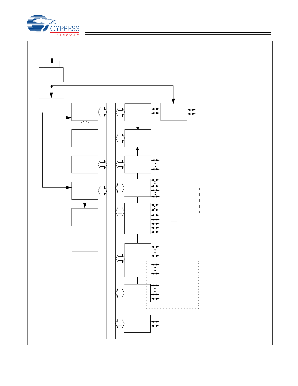
Logic Block Diagram
6-MHz crystal
PLL
48 MHz
CY7C64013C
CY7C64113C
Clock
Divider
6 MHz
12 MHz
12-MHz
8-bit
CPU
PROM
8 KB
RAM
256 byte
12-bit
Timer
Watchdog
Timer
Power-On
Reset
8-bit Bus
USB
SIE
Interrupt
Controller
GPIO
PORT 0
GPIO
PORT 1
GPIO/
HAPI
PORT 2
GPIO
USB
Transceiver
P0[7:0]
P1[2:0]
P1[7:3]
CY7C64113C only
P2[0,1,7]
P2[2]; Latch_Empty
P2[3]; Data_Ready
P2[4]; STB
P2[5]; OE
P2[6]; CS
High Current
P3[2:0]
Outputs
D+[0]
D–[0]
Upstream
USB Port
PORT 3
DAC
PORT
CY7C64113C only
I2C
Interface
*I2C-compatible interface enabled by firmware through
P2[1:0] or P1[1:0]
P3[7:3]
DAC[0]
DAC[2]
DAC[7]
SCLK
SDATA
Additional
High Current
Outputs
Document #: 38-08001 Rev. *B Page 8 of 51
[+] Feedback
Page 9
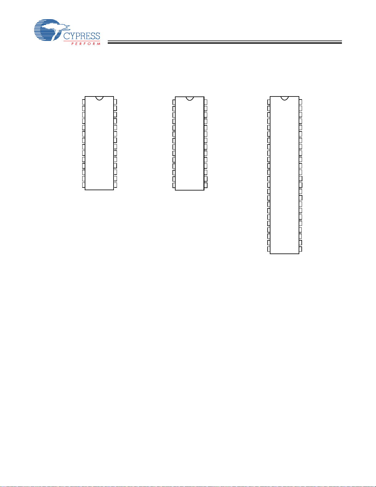
3.0 Pin Configurations
TOP VIEW
CY7C64013C
CY7C64113C
XTALOUT
XTALIN
V
REF
GND
P3[1]
D+[0]
D–[0]
P2[3]
P2[5]
P0[7]
P0[5]
P0[3]
P0[1]
P0[6]
CY7C64013C
28-pin SOIC
28
1
2
27
26
3
4
25
5
24
23
6
7
22
8
21
9
20
19
10
11
18
12
17
13
16
15
14
V
CC
P1[1]
P1[0]
P1[2]
P3[0]
P3[2]
GND
P2[2]
P2[4]
P2[6]
V
PP
P0[0]
P0[2]
P0[4]
XTALOUT
XTALIN
V
REF
P1[1]
GND
P3[1]
D+[0]
D–[0]
P2[3]
P2[5]
P0[7]
P0[5]
P0[3]
P0[1]
CY7C64013C
28-pin PDIP
1
28
2
27
26
3
4
25
5
24
23
6
7
22
8
21
9
20
19
10
11
18
12
17
13
16
15
14
V
CC
P1[0]
P1[2]
P3[0]
P3[2]
P2[2]
GND
P2[4]
P2[6]
V
PP
P0[0]
P0[2]
P0[4]
P0[6]
XTALOUT
XTALIN
V
REF
P1[3]
P1[5]
P1[7]
P3[1]
D+[0]
D–[0]
P3[3]
GND
P3[5]
P3[7]
P2[1]
P2[3]
GND
P2[5]
P2[7]
DAC[7]
P0[7]
P0[5]
P0[3]
P0[1]
DAC[1]
CY7C64113C
48-pin SSOP
48
1
2
47
46
3
4
45
5
44
43
6
7
42
8
41
9
40
39
10
11
38
12
37
13
36
35
14
15
34
16
33
17
32
18
31
19
30
29
20
21
28
22
27
23
26
24 25
V
CC
P1[1]
P1[0]
P1[2]
P1[4]
P1[6]
P3[0]
P3[2]
GND
P3[4]
NC
P3[6]
P2[0]
P2[2]
GND
P2[4]
P2[6]
DAC[0]
V
PP
P0[0]
P0[2]
P0[4]
P0[6]
DAC[2]
Document #: 38-08001 Rev. *B Page 9 of 51
[+] Feedback
Page 10

CY7C64013C
CY7C64113C
4.0 Product Summary Tables
4.1 Pin Assignments
Table 4-1. Pin Assignments
Name I/O 28-Pin SOIC 28-Pin PDIP 48-Pin SSOP Description
D+[0], D–[0] I/O 6, 7 7, 8 7, 8 Upstream port, USB differential data.
P0 I/O P0[7:0]
10, 14, 11, 15,
12, 16, 13, 17
P1 I/O P1[2:0]
25, 27, 26
P2 I/O P2[6:2]
19, 9, 20, 8,
21
P3 I/O P3[2:0]
23, 5, 24
DAC I/O DAC[7,2:0]
XTAL
IN
XTAL
OUT
V
PP
V
CC
GND IN 4, 22 5, 22 11, 16, 34, 40 Ground.
V
REF
NC 38 No Connect.
IN 2 2 2 6-MHz crystal or external clock input.
OUT 1 1 1 6-MHz crystal out.
IN 18 19 30 Programming voltage supply, tie to ground during
IN 28 28 48 Voltage supply.
IN 3 3 3 External 3.3V supply voltage for the differential data
P0[7:0]
11, 15, 12, 16,
13, 17, 14, 18
P1[2:0]
26, 4, 27
P2[6:2]
20, 10, 21,
9, 23
P3[2:0]
24, 6, 25
P0[7:0]
20, 26, 21, 27,
22, 28, 23, 29
P1[7:0]
6, 43, 5, 44,
4, 45, 47, 46
P2[7:0]
18, 32, 17, 33,
15, 35, 14, 36
P3[7:0]
13, 37, 12, 39,
10, 41, 7, 42
19, 25, 24, 31
GPIO Port 0 capable of sinking 7 mA (typical).
GPIO Port 1 capable of sinking 7 mA (typical).
GPIO Port 2 capable of sinking 7 mA (typical). HAPI
is also supported through P2[6:2].
GPIO Port 3, capable of sinking 12 mA (typical).
DAC Port with programmable current sink outputs.
DAC[1:0] offer a programmable range of 3.2 to 16 mA
typical. DAC[7,2] have a programmable sink current
range of 0.2 to 1.0 mA typical.
normal operation.
output buffers and the D+ pull-up.
4.2 I/O Register Summary
I/O registers are accessed via the I/O Read (IORD) and I/O Write (IOWR, IOWX) instructions. IORD reads data from the selected
port into the accumulator. IOWR performs the reverse; it writes data from the accumulator to the selected port. Indexed I/O Write
(IOWX) adds the contents of X to the address in the instruction to form the port address and writes data from the accumulator to
the specified port. Specifying address 0 (e.g., IOWX 0h) means the I/O register is selected solely by the contents of X.
All undefined registers are reserved. It is important not to write to reserved registers as this may cause an undefined operation
or increased current consumption during operation. When writing to registers with reserved bits, the reserved bits must be written
with ‘0.’
Table 4-2. I/O Register Summary
Register Name I/O Address Read/Write Function Page
Port 0 Data 0x00 R/W GPIO Port 0 Data 19
Port 1 Data 0x01 R/W GPIO Port 1 Data 19
Port 2 Data 0x02 R/W GPIO Port 2 Data 19
Port 3 Data 0x03 R/W GPIO Port 3 Data 20
Port 0 Interrupt Enable 0x04 W Interrupt Enable for Pins in Port 0 21
Port 1 Interrupt Enable 0x05 W Interrupt Enable for Pins in Port 1 21
Port 2 Interrupt Enable 0x06 W Interrupt Enable for Pins in Port 2 21
Port 3 Interrupt Enable 0x07 W Interrupt Enable for Pins in Port 3 21
Document #: 38-08001 Rev. *B Page 10 of 51
[+] Feedback
Page 11

CY7C64013C
CY7C64113C
Table 4-2. I/O Register Summary (continued)
Register Name I/O Address Read/Write Function Page
GPIO Configuration 0x08 R/W GPIO Port Configurations 20
HAPI and I2C Configuration 0x09 R/W HAPI Width and I2C Position Configuration 24
USB Device Address A 0x10 R/W USB Device Address A 34
EP A0 Counter Register 0x11 R/W USB Address A, Endpoint 0 Counter 35
EP A0 Mode Register 0x12 R/W USB Address A, Endpoint 0 Configuration 34
EP A1 Counter Register 0x13 R/W USB Address A, Endpoint 1 Counter 35
EP A1 Mode Register 0x14 R/W USB Address A, Endpoint 1 Configuration 35
EP A2 Counter Register 0x15 R/W USB Address A, Endpoint 2 Counter 35
EP A2 Mode Register 0x16 R/W USB Address A, Endpoint 2 Configuration 35
USB Status & Control 0x1F R/W USB Upstream Port Traffic Status and Control 34
Global Interrupt Enable 0x20 R/W Global Interrupt Enable 29
Endpoint Interrupt Enable 0x21 R/W USB Endpoint Interrupt Enables 29
Timer (LSB) 0x24 R Lower 8 Bits of Free-running Timer (1 MHz) 23
Timer (MSB) 0x25 R Upper 4 Bits of Free-running Timer 24
WDT Clear 0x26 W Watchdog Timer Clear 18
2
C Control & Status 0x28 R/W I2C Status and Control 25
I
2
C Data 0x29 R/W I2C Data 25
I
DAC Data 0x30 R/W DAC Data 22
DAC Interrupt Enable 0x31 W Interrupt Enable for each DAC Pin 23
DAC Interrupt Polarity 0x32 W Interrupt Polarity for each DAC Pin 23
DAC Isink 0x38-0x3F W Input Sink Current Control for each DAC Pin 22
Reserved 0x40 Reserved
EP A3 Counter Register 0x41 R/W USB Address A, Endpoint 3 Counter 35
EP A3 Mode Register 0x42 R/W USB Address A, Endpoint 3 Configuration 34
EP A4 Counter Register 0x43 R/W USB Address A, Endpoint 4 Counter 35
EP A4 Mode Register 0x44 R/W USB Address A, Endpoint 4 Configuration 35
Reserved 0x48 Reserved
Reserved 0x49 Reserved
Reserved 0x4A Reserved
Reserved 0x4B Reserved
Reserved 0x4C Reserved
Reserved 0x4D Reserved
Reserved 0x4E Reserved
Reserved 0x4F Reserved
Reserved 0x50 Reserved
Reserved 0x51 Reserved
Processor Status & Control 0xFF R/W Microprocessor Status and Control Register 26
Document #: 38-08001 Rev. *B Page 11 of 51
[+] Feedback
Page 12

CY7C64013C
CY7C64113C
4.3 Instruction Set Summary
Refer to the CYASM Assembler User’s Guide for more details.
Table 4-3. Instruction Set Summary
MNEMONIC operand opcode cycles MNEMONIC operand opcode cycles
HALT 00 7 NOP 20 4
ADD A,expr data 01 4 INC A acc 21 4
ADD A,[expr] direct 02 6 INC X x 22 4
ADD A,[X+expr] index 03 7 INC [expr] direct 23 7
ADC A,expr data 04 4 INC [X+expr] index 24 8
ADC A,[expr] direct 05 6 DEC A acc 25 4
ADC A,[X+expr] index 06 7 DEC X x 26 4
SUB A,expr data 07 4 DEC [expr] direct 27 7
SUB A,[expr] direct 08 6 DEC [X+expr] index 28 8
SUB A,[X+expr] index 09 7 IORD expr address 29 5
SBB A,expr data 0A 4 IOWR expr address 2A 5
SBB A,[expr] direct 0B 6 POP A 2B 4
SBB A,[X+expr] index 0C 7 POP X 2C 4
OR A,expr data 0D 4 PUSH A 2D 5
OR A,[expr] direct 0E 6 PUSH X 2E 5
OR A,[X+expr] index 0F 7 SWAP A,X 2F 5
AND A,expr data 10 4 SWAP A,DSP 30 5
AND A,[expr] direct 11 6 MOV [expr],A direct 31 5
AND A,[X+expr] index 12 7 MOV [X+expr],A index 32 6
XOR A,expr data 13 4 OR [expr],A direct 33 7
XOR A,[expr] direct 14 6 OR [X+expr],A index 34 8
XOR A,[X+expr] index 15 7 AND [expr],A direct 35 7
CMP A,expr data 16 5 AND [X+expr],A index 36 8
CMP A,[expr] direct 17 7 XOR [expr],A direct 37 7
CMP A,[X+expr] index 18 8 XOR [X+expr],A index 38 8
MOV A,expr data 19 4 IOWX [X+expr] index 39 6
MOV A,[expr] direct 1A 5 CPL 3A 4
MOV A,[X+expr] index 1B 6 ASL 3B 4
MOV X,expr data 1C 4 ASR 3C 4
MOV X,[expr] direct 1D 5 RLC 3D 4
reserved 1E RRC 3E 4
XPAGE 1F 4 RET 3F 8
MOV A,X 40 4 DI 70 4
MOV X,A 41 4 EI 72 4
MOV PSP,A 60 4 RETI 73 8
CALL addr 50 - 5F 10 JC addr C0-CF 5
JMP addr 80-8F 5 JNC addr D0-DF 5
CALL addr 90-9F 10 JACC addr E0-EF 7
JZ addr A0-AF 5 INDEX addr F0-FF 14
JNZ addr B0-BF 5
Document #: 38-08001 Rev. *B Page 12 of 51
[+] Feedback
Page 13

CY7C64013C
CY7C64113C
5.0 Programming Model
5.1 14-Bit Program Counter (PC)
The 14-bit program counter (PC) allows access to up to 8 KB of PROM available with the CY7C64x13C architecture. The top 32
bytes of the ROM in the 8 Kb part are reserved for testing purposes. The program counter is cleared during reset, such that the
first instruction executed after a reset is at address 0x0000h. Typically, this is a jump instruction to a reset handler that initializes
the application (see Interrupt Vectors on page 30).
The lower eight bits of the program counter are incremented as instructions are loaded and executed. The upper six bits of the
program counter are incremented by executing an XPAGE instruction. As a result, the last instruction executed within a 256-byte
“page” of sequential code should be an XPAGE instruction. The assembler directive “XPAGEON” causes the assembler to insert
XPAGE instructions automatically. Because instructions can be either one or two bytes long, the assembler may occasionally
need to insert a NOP followed by an XPAGE to execute correctly.
The address of the next instruction to be executed, the carry flag, and the zero flag are saved as two bytes on the program stack
during an interrupt acknowledge or a CALL instruction. The program counter, carry flag, and zero flag are restored from the
program stack during a RETI instruction. Only the program counter is restored during a RET instruction.
The program counter cannot be accessed directly by the firmware. The program stack can be examined by reading SRAM from
location 0x00 and up.
Document #: 38-08001 Rev. *B Page 13 of 51
[+] Feedback
Page 14

5.1.1 Program Memory Organization
after reset Address
14-bit PC 0x0000 Program execution begins here after a reset
0x0002 USB Bus Reset interrupt vector
0x0004 128-µs timer interrupt vector
0x0006 1.024-ms timer interrupt vector
0x0008 USB address A endpoint 0 interrupt vector
0x000A USB address A endpoint 1 interrupt vector
0x000C USB address A endpoint 2 interrupt vector
0x000E USB address A endpoint 3 interrupt vector
CY7C64013C
CY7C64113C
0x0010 USB address A endpoint 4 interrupt vector
0x0012 Reserved
0x0014 DAC interrupt vector
0x0016 GPIO interrupt vector
0x0018
0x001A
2
I
C interrupt vector
Program Memory begins here
0x1FDF 8 KB (-32) PROM ends here (CY7C64013C, CY7C64113C)
Document #: 38-08001 Rev. *B Page 14 of 51
[+] Feedback
Page 15
CY7C64013C
CY7C64113C
5.2 8-Bit Accumulator (A)
The accumulator is the general-purpose register for the microcontroller.
5.3 8-Bit Temporary Register (X)
The “X” register is available to the firmware for temporary storage of intermediate results. The microcontroller can perform indexed
operations based on the value in X. Refer to Section 5.6.3 for additional information.
5.4 8-Bit Program Stack Pointer (PSP)
During a reset, the program stack pointer (PSP) is set to 0x00 and “grows” upward from this address. The PSP may be set by
firmware, using the MOV PSP,A instruction. The PSP supports interrupt service under hardware control and CALL, RET, and
RETI instructions under firmware control. The PSP is not readable by the firmware.
During an interrupt acknowledge, interrupts are disabled and the 14-bit program counter, carry flag, and zero flag are written as
two bytes of data memory. The first byte is stored in the memory addressed by the PSP, then the PSP is incremented. The second
byte is stored in memory addressed by the PSP, and the PSP is incremented again. The overall effect is to store the program
counter and flags on the program “stack” and increment the PSP by two.
The Return from Interrupt (RETI) instruction decrements the PSP, then restores the second byte from memory addressed by the
PSP. The PSP is decremented again and the first byte is restored from memory addressed by the PSP. After the program counter
and flags have been restored from stack, the interrupts are enabled. The overall effect is to restore the program counter and flags
from the program stack, decrement the PSP by two, and reenable interrupts.
The Call Subroutine (CALL) instruction stores the program counter and flags on the program stack and increments the PSP by
two.
The Return from Subroutine (RET) instruction restores the program counter but not the flags from the program stack and decrements the PSP by two.
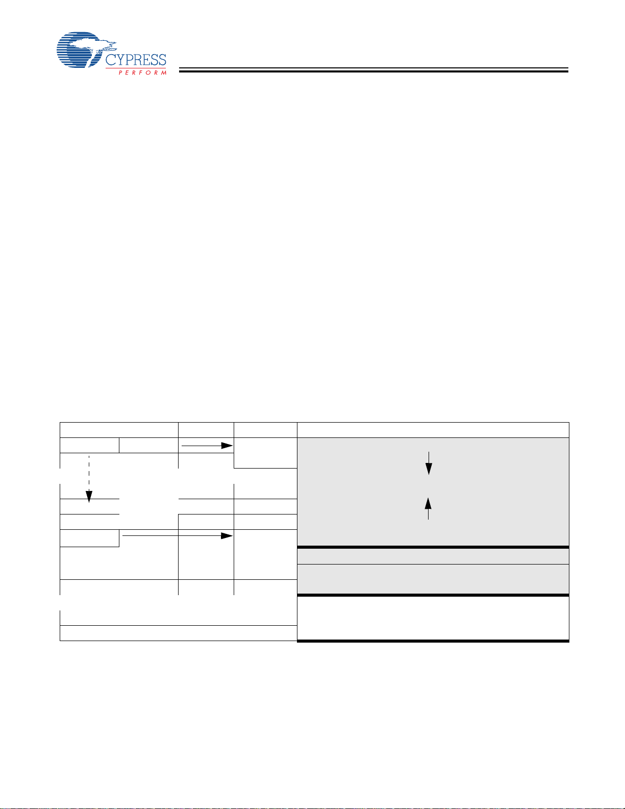
5.4.1 Data Memory Organization
The CY7C64x13C microcontrollers provide 256 bytes of data RAM. Normally, the SRAM is partitioned into four areas: program
stack, user variables, data stack, and USB endpoint FIFOs. The following is one example of where the program stack, data stack,
and user variables areas could be located.
After reset Address
8-bit DSP 8-bit PSP 0x00 Program Stack Growth
(Move DSP
8-bit DSP
Notes:
1. Refer to Section 5.5 for a description of DSP.
2. Endpoint sizes are fixed by the Endpoint Size Bit (I/O register 0x1F, Bit 7), see Table 18-1.
[1]
)
user selected Data Stack Growth
User variables
USB FIFO space for five endpoints
0xFF
[2]
Document #: 38-08001 Rev. *B Page 15 of 51
[+] Feedback
Page 16

CY7C64013C
CY7C64113C
5.5 8-Bit Data Stack Pointer (DSP)
The data stack pointer (DSP) supports PUSH and POP instructions that use the data stack for temporary storage. A PUSH
instruction pre-decrements the DSP, then writes data to the memory location addressed by the DSP. A POP instruction reads
data from the memory location addressed by the DSP, then post-increments the DSP.
During a reset, the DSP is reset to 0x00. A PUSH instruction when DSP equals 0x00 writes data at the top of the data RAM
(address 0xFF). This writes data to the memory area reserved for USB endpoint FIFOs. Therefore, the DSP should be indexed
at an appropriate memory location that does not compromise the Program Stack, user-defined memory (variables), or the USB
endpoint FIFOs.
For USB applications, the firmware should set the DSP to an appropriate location to avoid a memory conflict with RAM dedicated
to USB FIFOs. The memory requirements for the USB endpoints are described in Section 18.2. Example assembly instructions
to do this with two device addresses (FIFOs begin at 0xD8) are shown below:
MOV A,20h ; Move 20 hex into Accumulator (must be D8h or less)
SWAP A,DSP ; swap accumulator value into DSP register
5.6 Address Modes
The CY7C64013C and CY7C64113C microcontrollers support three addressing modes for instructions that require data
operands: data, direct, and indexed.
5.6.1 Data (Immediate)
“Data” address mode refers to a data operand that is actually a constant encoded in the instruction. As an example, consider the
instruction that loads A with the constant 0xD8:
• MOV A,0D8h
This instruction requires two bytes of code where the first byte identifies the “MOV A” instruction with a data operand as the
second byte. The second byte of the instruction is the constant “0xD8.” A constant may be referred to by name if a prior “EQU”
statement assigns the constant value to the name. For example, the following code is equivalent to the example shown above:
• DSPINIT: EQU 0D8h
• MOV A,DSPINIT
5.6.2 Direct
“Direct” address mode is used when the data operand is a variable stored in SRAM. In that case, the one byte address of the
variable is encoded in the instruction. As an example, consider an instruction that loads A with the contents of memory address
location 0x10:
• MOV A,[10h]
Normally, variable names are assigned to variable addresses using “EQU” statements to improve the readability of the assembler
source code. As an example, the following code is equivalent to the example shown above:
• buttons: EQU 10h
• MOV A,[buttons]
5.6.3 Indexed
“Indexed” address mode allows the firmware to manipulate arrays of data stored in SRAM. The address of the data operand is
the sum of a constant encoded in the instruction and the contents of the “X” register. Normally, the constant is the “base” address
of an array of data and the X register contains an index that indicates which element of the array is actually addressed:
•array: EQU 10h
•MOV X,3
• MOV A,[X+array]
This would have the effect of loading A with the fourth element of the SRAM “array” that begins at address 0x10. The fourth
element would be at address 0x13.
Document #: 38-08001 Rev. *B Page 16 of 51
[+] Feedback
Page 17

6.0 Clocking
XTALOUT
(pin 1)
CY7C64013C
CY7C64113C
XTALIN
(pin 2)
30 pF
Figure 6-1. Clock Oscillator On-Chip Circuit
The XTALIN and XTALOUT are the clock pins to the microcontroller. The user can connect an external oscillator or a crystal to
these pins. When using an external crystal, keep PCB traces between the chip leads and crystal as short as possible (less than
2 cm). A 6-MHz fundamental frequency parallel resonant crystal can be connected to these pins to provide a reference frequency
for the internal PLL. The two internal 30-pF load caps appear in series to the external crystal and would be equivalent to a 15-pF
load. Therefore, the crystal must have a required load capacitance of about 15–18 pF. A ceramic resonator does not allow the
microcontroller to meet the timing specifications of full speed USB and therefore a ceramic resonator is not recommended with
these parts.
An external 6-MHz clock can be applied to the XTALIN pin if the XTALOUT pin is left open. Grounding the XTALOUT pin when
driving XTALIN with an oscillator does not work because the internal clock is effectively shorted to ground.
To Internal PLL
30 pF
7.0 Reset
The CY7C64x13C supports two resets: Power-On Reset (POR) and a Watchdog Reset (WDR). Each of these resets causes:
• all registers to be restored to their default states,
• the USB Device Address to be set to 0,
• all interrupts to be disabled,
• the PSP and Data Stack Pointer (DSP) to be set to memory address 0x00.
The occurrence of a reset is recorded in the Processor Status and Control Register, as described in Section 15.0. Bits 4 and 6
are used to record the occurrence of POR and WDR, respectively. Firmware can interrogate these bits to determine the cause
of a reset.
Program execution starts at ROM address 0x0000 after a reset. Although this looks like interrupt vector 0, there is an important
difference. Reset processing does NOT push the program counter, carry flag, and zero flag onto program stack. The firmware
reset handler should configure the hardware before the “main” loop of code. Attempting to execute a RET or RETI in the firmware
reset handler causes unpredictable execution results.
7.1 Power-On Reset (POR)
When VCC is first applied to the chip, the Power-On Reset (POR) signal is asserted and the CY7C64x13C enters a “semi-suspend”
state. During the semi-suspend state, which is different from the suspend state defined in the USB specification, the oscillator
and all other blocks of the part are functional, except for the CPU. This semi-suspend time ensures that both a valid VCC level is
reached and that the internal PLL has time to stabilize before full operation begins. When the V
2.5V, and the oscillator is stable, the POR is deasserted and the on-chip timer starts counting. The first 1 ms of suspend time is
not interruptible, and the semi-suspend state continues for an additional 95 ms unless the count is bypassed by a USB Bus Reset
on the upstream port. The 95 ms provides time for V
If a USB Bus Reset occurs on the upstream port during the 95-ms semi-suspend time, the semi-suspend state is aborted and
program execution begins immediately from address 0x0000. In this case, the Bus Reset interrupt is pending but not serviced
until firmware sets the USB Bus Reset Interrupt Enable bit (bit 0 of register 0x20) and enables interrupts with the EI command.
The POR signal is asserted whenever V
again. Behavior is the same as described above.
drops below approximately 2.5V, and remains asserted until VCC rises above this level
CC
to stabilize at a valid operating voltage before the chip executes code.
CC
has risen above approximately
CC
7.2 Watchdog Reset (WDR)
The Watchdog Timer Reset (WDR) occurs when the internal Watchdog timer rolls over. Writing any value to the write-only
Watchdog Restart Register at address 0x26 clears the timer. The timer rolls over and WDR occurs if it is not cleared within t
(8 ms minimum) of the last clear. Bit 6 of the Processor Status and Control Register is set to record this event (the register contents
are set to 010X0001 by the WDR). A Watchdog Timer Reset lasts for 2 ms, after which the microcontroller begins execution at
ROM address 0x0000.
Document #: 38-08001 Rev. *B Page 17 of 51
WATCH
[+] Feedback
Page 18

CY7C64013C
CY7C64113C
t
WATCH
Last write to
Watchdog Timer
Register
The USB transmitter is disabled by a Watchdog Reset because the USB Device Address Register is cleared (see Section 18.1).
Otherwise, the USB Controller would respond to all address 0 transactions.
It is possible for the WDR bit of the Processor Status and Control Register (0xFF) to be set following a POR event. The WDR bit
should be ignored If the firmware interrogates the Processor Status and Control Register for a Set condition on the WDR bit and
if the POR (bit 3 of register 0xFF) bit is set.
No write to WDT
register, so WDR
goes HIGH
Figure 7-1. Watchdog Reset (WDR)
2 ms
Execution begins at
Reset Vector 0x0000
8.0 Suspend Mode
The CY7C64x13C can be placed into a low-power state by setting the Suspend bit of the Processor Status and Control register.
All logic blocks in the device are turned off except the GPIO interrupt logic and the USB receiver. The clock oscillator and PLL,
as well as the free-running and Watchdog timers, are shut down. Only the occurrence of an enabled GPIO interrupt or non-idle
bus activity at a USB upstream or downstream port wakes the part out of suspend. The Run bit in the Processor Status and
Control Register must be set to resume a part out of suspend.
The clock oscillator restarts immediately after exiting suspend mode. The microcontroller returns to a fully functional state 1 ms
after the oscillator is stable. The microcontroller executes the instruction following the I/O write that placed the device into suspend
mode before servicing any interrupt requests.
The GPIO interrupt allows the controller to wake-up periodically and poll system components while maintaining a very low average
power consumption. To achieve the lowest possible current during suspend mode, all I/O should be held at V
applies to internal port pins that may not be bonded in a particular package.
Typical code for entering suspend is shown below:
... ; All GPIO set to low-power state (no floating pins)
... ; Enable GPIO interrupts if desired for wake-up
mov a, 09h ; Set suspend and run bits
iowr FFh ; Write to Status and Control Register - Enter suspend, wait for USB activity (or GPIO Interrupt)
nop ; This executes before any ISR
... ; Remaining code for exiting suspend routine
or Gnd. This also
CC
Document #: 38-08001 Rev. *B Page 18 of 51
[+] Feedback
Page 19

9.0 General-Purpose I/O (GPIO) Ports
GPIO
CFG
OE
mode
2-bits
Q1
CY7C64013C
CY7C64113C
V
CC
Q2
Internal
Data Bus
Port Write
Port Read
Reg_Bit
STRB
(Latch is Transparent
except in HAPI mode)
Interrupt
Enable
Interrupt
Controller
Data
Out
Latch
Data
In
Latch
Data
Interrupt
Latch
Control
Control
14 kΩ
Q3*
GPIO
PIN
*Port 0,1,2: Low I
Port 3: High I
sink
sink
Figure 9-1. Block Diagram of a GPIO Pin
There are up to 32 GPIO pins (P0[7:0], P1[7:0], P2[7:0], and P3[7:0]) for the hardware interface. The number of GPIO pins
changes based on the package type of the chip. Each port can be configured as inputs with internal pull-ups, open drain outputs,
or traditional CMOS outputs. Port 3 offers a higher current drive, with typical current sink capability of 12 mA. The data for each
GPIO port is accessible through the data registers. Port data registers are shown in Figure 9-2 through Figure 9-5, and are set
to 1 on reset.
Port 0 Data ADDRESS 0x00
Bit # 76543210
Bit Name P0.7 P0.6 P0.5 P0.4 P0.3 P0.2 P0.1 P0.0
Read/Write R/W R/W R/W R/W R/W R/W R/W R/W
Reset 11111111
Figure 9-2. Port 0 Data
Port 1 Data ADDRESS 0x01
Bit # 76543210
Bit Name P1.7 P1.6 P1.5 P1.4 P1.3 P1.2 P1.1 P1.0
Read/Write R/W R/W R/W R/W R/W R/W R/W R/W
Reset 11111111
Figure 9-3. Port 1 Data
Port 2 Data ADDRESS 0x02
Bit # 76543210
Bit Name P2.7 P2.6 P2.5 P2.4 P2.3 P2.2 P2.1 P2.0
Read/Write R/W R/W R/W R/W R/W R/W R/W R/W
Reset 11111111
Figure 9-4. Port 2 Data
Document #: 38-08001 Rev. *B Page 19 of 51
[+] Feedback
Page 20

CY7C64013C
CY7C64113C
Port 3 Data ADDRESS 0x03
Bit # 76543210
Bit Name P3.7 P3.6 P3.5 P3.4 P3.3 P32 P3.1 P3.0
Read/Write R/W R/W R/W R/W R/W R/W R/W R/W
Reset 11111111
Figure 9-5. Port 3 Data
Special care should be taken with any unused GPIO data bits. An unused GPIO data bit, either a pin on the chip or a port bit that
is not bonded on a particular package, must not be left floating when the device enters the suspend state. If a GPIO data bit is
left floating, the leakage current caused by the floating bit may violate the suspend current limitation specified by the USB
Specifications. If a ‘1’ is written to the unused data bit and the port is configured with open drain outputs, the unused data bit
remains in an indeterminate state. Therefore, if an unused port bit is programmed in open-drain mode, it must be written with a
‘0.’ Notice that the CY7C64013C part always requires that the data bits P1[7:3], P2[7,1,0], and P3[7:3] be written with a ‘0.’
In normal non-HAPI mode, reads from a GPIO port always return the present state of the voltage at the pin, independent of the
settings in the Port Data Registers. If HAPI mode is activated for a port, reads of that port return latched data as controlled by the
HAPI signals (see Section 14.0). During reset, all of the GPIO pins are set to a high-impedance input state (‘1’ in open drain
mode). Writing a ‘0’ to a GPIO pin drives the pin LOW. In this state, a ‘0’ is always read on that GPIO pin unless an external source
overdrives the internal pull-down device.
9.1 GPIO Configuration Port
Every GPIO port can be programmed as inputs with internal pull-ups, outputs LOW or HIGH, or Hi-Z (floating, the pin is not driven
internally). In addition, the interrupt polarity for each port can be programmed. The Port Configuration bits (Figure 9-6) and the
Interrupt Enable bit (Figure 9-7 through Figure 9-10) determine the interrupt polarity of the port pins.
GPIO Configuration ADDRESS 0x08
Bit # 76543210
Bit Name Port 3
Read/Write R/W R/W R/W R/W R/W R/W R/W R/W
Reset 00000000
Config Bit 1
Port 3
Config Bit 0
Port 2
Config Bit 1
Port 2
Config Bit 0
Port 1
Config Bit 1
Port 1
Config Bit 0
Port 0
Config Bit 1
Port 0
Config Bit 0
Figure 9-6. GPIO Configuration Register
As shown in Table 9-1 below, a positive polarity on an input pin represents a rising edge interrupt (LOW to HIGH), and a negative
polarity on an input pin represents a falling edge interrupt (HIGH to LOW).
The GPIO interrupt is generated when all of the following conditions are met: the Interrupt Enable bit of the associated Port
Interrupt Enable Register is enabled, the GPIO Interrupt Enable bit of the Global Interrupt Enable Register (Figure 16-1) is
enabled, the Interrupt Enable Sense (bit 2, Figure 15-1) is set, and the GPIO pin of the port sees an event matching the interrupt
polarity.
The driving state of each GPIO pin is determined by the value written to the pin’s Data Register (Figure 9-2 through Figure 9-5)
and by its associated Port Configuration bits as shown in the GPIO Configuration Register (Figure 9-6). These ports are configured
on a per-port basis, so all pins in a given port are configured together. The possible port configurations are detailed in Table 9-1.
As shown in this table below, when a GPIO port is configured with CMOS outputs, interrupts from that port are disabled.
During reset, all of the bits in the GPIO Configuration Register are written with ‘0’ to select Hi-Z mode for all GPIO ports as the
default configuration.
Table 9-1. GPIO Port Output Control Truth Table and Interrupt Polarity
Port Config Bit 1 Port Config Bit 0 Data Register Output Drive Strength Interrupt Enable Bit Interrupt Polarity
1 1 0 Output LOW 0 Disabled
1 Resistive 1 – (Falling Edge)
1 0 0 Output LOW 0 Disabled
1 Output HIGH 1 Disabled
0 1 0 Output LOW 0 Disabled
1 Hi-Z 1 – (Falling Edge)
0 0 0 Output LOW 0 Disabled
1 Hi-Z 1 + (Rising Edge)
Document #: 38-08001 Rev. *B Page 20 of 51
[+] Feedback
Page 21

CY7C64013C
CY7C64113C
Q1, Q2, and Q3 discussed below are the transistors referenced in Figure 9-1. The available GPIO drive strength are:
• Output LOW Mode: The pin’s Data Register is set to ‘0’
Writing ‘0’ to the pin’s Data Register puts the pin in output LOW mode, regardless of the contents of the Port Configuration
Bits[1:0]. In this mode, Q1 and Q2 are OFF. Q3 is ON. The GPIO pin is driven LOW through Q3.
• Output HIGH Mode: The pin’s Data Register is set to 1 and the Port Configuration Bits[1:0] is set to ‘10’
In this mode, Q1 and Q3 are OFF. Q2 is ON. The GPIO is pulled up through Q2. The GPIO pin is capable of sourcing... of
current.
• Resistive Mode: The pin’s Data Register is set to 1 and the Port Configuration Bits[1:0] is set to ‘11’
Q2 and Q3 are OFF. Q1 is ON. The GPIO pin is pulled up with an internal 14kΩ resistor. In resistive mode, the pin may serve
as an input. Reading the pin’s Data Register returns a logic HIGH if the pin is not driven LOW by an external source.
• Hi-Z Mode: The pin’s Data Register is set to1 and Port Configuration Bits[1:0] is set either ‘00’ or ‘01’
Q1, Q2, and Q3 are all OFF. The GPIO pin is not driven internally. In this mode, the pin may serve as an input. Reading the
Port Data Register returns the actual logic value on the port pins.
9.2 GPIO Interrupt Enable Ports
Each GPIO pin can be individually enabled or disabled as an interrupt source. The Port 0–3 Interrupt Enable registers provide
this feature with an interrupt enable bit for each GPIO pin. When HAPI mode (discussed in Section 14.0) is enabled the GPIO
interrupts are blocked, including ports not used by HAPI, so GPIO pins cannot be used as interrupt sources.
During a reset, GPIO interrupts are disabled by clearing all of the GPIO interrupt enable ports. Writing a ‘1’ to a GPIO Interrupt
Enable bit enables GPIO interrupts from the corresponding input pin. All GPIO pins share a common interrupt, as discussed in
Section 16.7
Port 0 Interrupt Enable ADDRESS 0x04
Bit # 76543210
Bit Name P0.7 Intr Enable P0.6 Intr Enable P0.5 Intr Enable P0.4 Intr Enable P0.3 Intr Enable P0.2 Intr Enable P0.1 Intr Enable P0.0 Intr Enable
Read/Write WWWWWWWW
Reset 00000000
Figure 9-7. Port 0 Interrupt Enable
Bit # 76543210
Bit Name P1.7 Intr Enable P1.6 Intr Enable P1.5 Intr Enable P1.4 Intr Enable P1.3 Intr Enabl P1.2 Intr Enable P1.1 Intr Enable P1.0 Intr Enable
Read/Write WWWWWWWW
Reset 00000000
Figure 9-8. Port 1 Interrupt Enable
Port 2 Interrupt Enable ADDRESS 0x06
Bit # 76543210
Bit Name P2.7 Intr Enable P2.6 Intr Enable P2.5 Intr Enable P2.4 Intr Enable P2.3 Intr Enable P2.2 Intr Enable P2.1 Intr Enable P2.0 Intr Enable
Read/Write WWWWWWWW
Reset 00000000
Figure 9-9. Port 2 Interrupt Enable
Port 3 Interrupt Enable ADDRESS 0x07
Bit # 76543210
Bit Name Reserved
Read/Write WWWWWWWW
Reset 00000000
(Set to 0)
P3.6 Intr Enable P3.5 Intr Enable P3.4 Intr Enable P3.3 Intr Enable P3.2 Intr Enable P3.1 Intr Enable P3.0 Intr Enable
Figure 9-10. Port 3 Interrupt Enable
10.0 DAC Port
The CY7C64113C features a programmable current sink 4 bit port which is also known as a DAC port. Each of these port I/O
pins have a programmable current sink. Writing a ‘1’ to a DAC I/O pin disables the output current sink (Isink DAC) and drives the
I/O pin HIGH through an integrated 14-kΩ resistor. When a ‘0’ is written to a DAC I/O pin, the Isink DAC is enabled and the pullup resistor is disabled. This causes the I
the DAC port pin.
DAC to sink current to drive the output LOW. Figure 10-1 shows a block diagram of
sink
Document #: 38-08001 Rev. *B Page 21 of 51
[+] Feedback
Page 22

CY7C64013C
CY7C64113C
V
CC
Internal
Data Bus
Data
Out
Latch
DAC Write
Suspend
(Bit 3 of Register 0xFF)
Q1
14 kΩ
DAC
I/O Pin
4 bits
Isink
DAC
to Interrupt
Controller
Interrupt
Enable
Interrupt
Polarity
Internal
Buffer
DAC Read
Isink
Register
Interrupt Logic
Figure 10-1. Block Diagram of a DAC Pin
The amount of sink current for the DAC I/O pin is programmable over 16 values based on the contents of the DAC Isink Register
for that output pin. DAC[1:0] are high-current outputs that are programmable from 3.2 mA to 16 mA (typical). DAC[7:2] are lowcurrent outputs, programmable from 0.2 mA to 1.0 mA (typical).
When the suspend bit in Processor Status and Control Register (see Figure 15-1) is set, the Isink DAC block of the DAC circuitry
is disabled. Special care should be taken when the CY7C64x13C device is placed in the suspend mode. The DAC Port Data
Register (see Figure 10-2) should normally be loaded with all ‘1’s (0xFF) before setting the suspend bit. If any of the DAC bits
are set to ‘0’ when the device is suspended, that DAC input will float. The floating pin could result in excessive current consumption
by the device, unless an external load places the pin in a deterministic state.
DAC Port Data ADDRESS 0x30
Bit # 76543210
Bit Name DAC[7] Reserved Reserved Reserved Reserved DAC[2] DAC[1] DAC[0]
Read/Write R/W R/W R/W R/W R/W R/W R/W R/W
Reset 11111111
Figure 10-2. DAC Port Data
Bit [1..0]: High Current Output 3.2 mA to 16 mA typical
1= I/O pin is an output pulled HGH through the 14-kΩ resistor. 0 = I/O pin is an input with an internal 14-kΩ pull-up resistor
Bit [3..2]: Low Current Output 0.2 mA to 1 mA typical
1= I/O pin is an output pulled HGH through the 14-kΩ resistor. 0 = I/O pin is an input with an internal 14-kΩ pull-up resistor
10.1 DAC Isink Registers
Each DAC I/O pin has an associated DAC Isink register to program the output sink current when the output is driven LOW. The
first Isink register (0x38) controls the current for DAC[0], the second (0x39) for DAC[1], and so on until the Isink register at 0x3F
controls the current to DAC[7].
DAC Sink Register ADDRESS 0x38 -0x3F
Bit # 76543210
Bit Name Reserved Reserved Reserved Reserved Isink[3] Isink[2] Isink[1] Isink[0]
Read/Write WWWW
Reset ----0000
Figure 10-3. DAC Sink Register
Document #: 38-08001 Rev. *B Page 22 of 51
[+] Feedback
Page 23

CY7C64013C
CY7C64113C
Bit [4..0]: Isink [x] (x= 0..4)
Writing all ‘0’s to the Isink register causes 1/5 of the max current to flow through the DAC I/O pin. Writing all ‘1’s to the
Isink register provides the maximum current flow through the pin. The other 14 states of the DAC sink current are evenly
spaced between these two values.
Bit [7..5]: Reserved
10.2 DAC Port Interrupts
A DAC port interrupt can be enabled/disabled for each pin individually. The DAC Port Interrupt Enable register provides this
feature with an interrupt enable bit for each DAC I/O pin.All of the DAC Port Interrupt Enable register bits are cleared to ‘0’ during
a reset. All DAC pins share a common interrupt, as explained in Section 16.6.
DAC Port Interrupt ADDRESS 0x31
Bit # 76543210
Bit Name Enable Bit 7 Reserved Reserved Reserved Reserved Enable Bit 2 Enable Bit 1 Enable Bit 0
Read/Write WWWWWWWW
Reset 00000000
Figure 10-4. DAC Port Interrupt Enable
Bit [7..0]: Enable bit x (x= 0..2, 7)
1= Enables interrupts from the corresponding bit position; 0= Disables interrupts from the corresponding bit position
As an additional benefit, the interrupt polarity for each DAC pin is programmable with the DAC Port Interrupt Polarity register.
Writing a ‘0’ to a bit selects negative polarity (falling edge) that causes an interrupt (if enabled) if a falling edge transition occurs
on the corresponding input pin. Writing a ‘1’ to a bit in this register selects positive polarity (rising edge) that causes an interrupt
(if enabled) if a rising edge transition occurs on the corresponding input pin. All of the DAC Port Interrupt Polarity register bits are
cleared during a reset.
DAC Port Interrupt Polarity ADDRESS 0x32
Bit # 76543210
Bit Name Enable Bit 7 Reserved Reserved Reserved Reserved Enable Bit 2 Enable Bit 1 Enable Bit 0
Read/Write WWWWWWWW
Reset 00000000
Figure 10-5. DAC Port Interrupt Polarity
Bit [7..0]: Enable bit x (x= 0..2, 7)
1= Selects positive polarity (rising edge) that causes an interrupt (if enabled);
0= Selects negative polarity (falling edge) that causes an interrupt (if enabled)
11.0 12-Bit Free-Running Timer
The 12-bit timer provides two interrupts (128-µs and 1.024-ms) and allows the firmware to directly time events that are up to 4
ms in duration. The lower 8 bits of the timer can be read directly by the firmware. Reading the lower 8 bits latches the upper 4
bits into a temporary register. When the firmware reads the upper 4 bits of the timer, it is accessing the count stored in the
temporary register. The effect of this logic is to ensure a stable 12-bit timer value can be read, even when the two reads are
separated in time.
Timer LSB ADDRESS 0x24
Bit # 76543210
Bit Name Timer Bit 7 Timer Bit 6 Timer Bit 5 Timer Bit 4 Timer Bit 3 Timer Bit 2 Timer Bit 1 Timer Bit 0
Read/Write RRRRRRRR
Reset 00000000
Figure 11-1. Timer LSB Register
Bit [7:0]: Timer lower 8 bits
Document #: 38-08001 Rev. *B Page 23 of 51
[+] Feedback
Page 24

CY7C64013C
CY7C64113C
Timer MSB ADDRESS 0x25
Bit # 76543210
Bit Name Reserved Reserved Reserved Reserved Timer Bit 11 Timer Bit 10 Timer Bit 9 Timer Bit 8
Read/Write ----RRRR
Reset 00000000
Figure 11-2. Timer MSB Register
Bit [3:0]: Timer higher nibble
Bit [7:4]: Reserved
1.024-ms Interrupt
µs Interrupt
128-
10 9 78
6432
5
1 011
1-MHz Clock
L1 L0L2L3
D3 D2 D1 D0 D7 D6 D5 D4 D3 D2 D1 D0
To Timer Register
8
Figure 11-3. Timer Block Diagram
12.0 I2C and HAPI Configuration Register
Internal hardware supports communication with external devices through two interfaces: a two-wire I2C-compatible interface, and
a HAPI for 1, 2, or 3 byte transfers. The I
14.0, share a common configuration register (see Figure 12-1). All bits of this register are cleared on reset.
2
I
C Configuration ADDRESS 0x09
Bit # 76543210
Bit Name I
Read/Write R/W - R/W R/W R R R/W R/W
Reset 00000000
2
C Position Reserved LEMPTY
2
C-compatible interface and HAPI functions, discussed in detail in Sections 13.0 and
Polarity
DRDY
Polarity
Latch
Empty
Data
Ready
HAPI Port Width
Bit 1
HAPI Port Width
Bit 0
Figure 12-1. HAPI/I2C Configuration Register
Note: I2C-compatible function must be separately enabled as described in Section 13.0.
Bits [7,1:0] of the HAPI/I
Bits [5:2] are used in HAPI mode only, and are described in Section 14.0. Table 12-1 shows the HAPI port configurations, and
Table 12-2 shows I
packages, and to allow simultaneous HAPI and I
HAPI operation is enabled whenever either HAPI Port Width Bit (Bit 1 or 0) is non-zero. This affects GPIO operation as described
in Section 14.0. I
2
2
C Configuration Register control the pin out configuration of the HAPI and I2C-compatible interfaces.
2
C pin location configuration options. These I2C-compatible options exist due to pin limitations in certain
2
C-compatible operation.
C-compatible blocks must be separately enabled as described in Section 13.0.
Document #: 38-08001 Rev. *B Page 24 of 51
[+] Feedback
Page 25

CY7C64013C
CY7C64113C
Table 12-1. HAPI Port Configuration
Port Width (Bits[1:0]) HAPI Port Width
11 24 Bits: P3[7:0], P1[7:0], P0[7:0]
10 16 Bits: P1[7:0], P0[7:0]
01 8 Bits: P0[7:0]
00 No HAPI Interface
Table 12-2. I
13.0 I2C-compatible Controller
The I2C-compatible block provides a versatile two-wire communication with external devices, supporting master, slave, and multimaster modes of operation. The I
interrupts as needed to allow firmware to take appropriate action during transactions. While waiting for firmware response, the
hardware keeps the I2C-compatible bus idle if necessary.
The I2C-compatible block generates an interrupt to the microcontroller at the end of each received or transmitted byte, when a
stop bit is detected by the slave when in receive mode, or when arbitration is lost. Details of the interrupt responses are given in
Section 16.8.
2
The I
(Figure 13-2). The Data Register is implemented as separate read and write registers. Generally, the I
Register should only be monitored after the I
read misleading bit status if a transaction is underway.
2
The I
1 or GPIO port 2. Refer to Section 12.0 for the bit definitions and functionality of the HAPI/I
used to set the locations of the configurable I
0 of the I
regardless of the settings of the GPIO Configuration Register.The electrical characteristics of the I
same as that of GPIO ports 1 and 2. Note that the I
All control of the I
I2C Data ADDRESS 0x29
Bit # 76543210
Bit Name I
Read/Write R/WR/WR/WR/WR/WR/WR/WR/W
Reset XXXXXXXX
2
C Port Configuration
2
C Position (Bit[7]) Port Width (Bit[1]) I2C Position
I
2
X1I
00I
10I
2
C-compatible block functions by handling the low-level signaling in hardware, and issuing
C-compatible interface consists of two registers, an I2C Data Register (Figure 13-1) and an I2C Status and Control Register
2
C interrupt, as all bits are valid at that time. Polling this register at other times could
C SCL clock is connected to bit 0 of GPIO port 1 or GPIO port 2, and the I2C SDA data is connected to bit 1 of GPIO port
2
2
C Status & Control Register, the two LSB bits ([1:0]) of the corresponding GPIO port are placed in Open Drain mode,
2
C clock and data lines is performed by the I2C-compatible block.
2
C Data 7 I2C Data 6 I2C Data 5 I2C Data 4 I2C Data 3 I2C Data 2 I2C Data 1 I2C Data 0
C-compatible pins. Once the I2C-compatible functionality is enabled by setting bit
(max) is 2 mA @ V
OL
= 2.0 V for ports 1 and 2.
OL
C on P2[1:0], 0:SCL, 1:SDA
2
C on P1[1:0], 0:SCL, 1:SDA
2
C on P2[1:0], 0:SCL, 1:SDA
2
C Status and Control
2
C Configuration Register, which is
2
C-compatible interface is the
Figure 13-1. I2C Data Register
Bits [7..0] : I2C Data
2
Contains the 8 bit data on the I
I2C Status and Control
Bit # 76543210
Bit Name MSTR Mode Continue/Busy Xmit Mode ACK Addr ARB
Read/Write R/WR/WR/WR/WR/WR/WR/WR/W
Reset 00000000
C Bus
Lost/Restart
Received Stop I
2
C Enable
Figure 13-2. I2C Status and Control Register
The I2C Status and Control register bits are defined in Table 14-1, with a more detailed description following.
Document #: 38-08001 Rev. *B Page 25 of 51
[+] Feedback
Page 26

CY7C64013C
CY7C64113C
Table 13-1. I2C Status and Control Register Bit Definitions
Bit Name Description
2
0I
1 Received Stop Reads 1 only in slave receive mode, when I
2 ARB Lost/Restart Reads 1 to indicate master has lost arbitration. Reads 0 otherwise.
3 Addr Reads 1 during first byte after start/restart in slave mode, or if master loses arbitration.
4 ACK In receive mode, write 1 to generate ACK, 0 for no ACK.
5 Xmit Mode Write to 1 for transmit mode, 0 for receive mode.
6 Continue/Busy Write 1 to indicate ready for next transaction.
7 MSTR Mode Write to 1 for master mode, 0 for slave mode. This bit is cleared if master loses arbitration.
Bit 7 : MSTR Mode
Bit 6 : Continue / Busy
Bit 5 : Xmit Mode
Bit 4 : ACK
Bit 3 : Addr
Bit 2 : ARB Lost/Restart
C Enable When set to ‘1’, the I2C-compatible function is enabled. When cleared, I2C GPIO pins
operate normally.
2
C Stop bit detected (unless firmware did not
ACK the last transaction).
Write to 1 in master mode to perform a restart sequence (also set Continue bit).
Reads 0 otherwise. This bit should always be written as 0.
In transmit mode, reads 1 if ACK was received, 0 if no ACK received.
2
Reads 1 when I
C-compatible block is busy with a transaction, 0 when transaction is
complete.
Clearing from 1 to 0 generates Stop bit.
2
Setting this bit to 1 causes the I
C-compatible block to initiate a master mode transaction by sending a start bit and
transmitting the first data byte from the data register (this typically holds the target address and R/W bit). Subsequent bytes
are initiated by setting the Continue bit, as described below.
Clearing this bit (set to 0) causes the GPIO pins to operate normally
In master mode, the I
transmit or receive state. The I
2
C-compatible block generates the clock (SCK), and drives the data line as required depending on
2
C-compatible block performs any required arbitration and clock synchronization. IN the
event of a loss of arbitration, this MSTR bit is cleared, the ARB Lost bit is set, and an interrupt is generated by the
microcontroller. If the chip is the target of an external master that wins arbitration, then the interrupt is held off until the
transaction from the external master is completed.
When MSTR Mode is cleared from 1 to 0 by a firmware write, an I
2
C Stop bit is generated.
This bit is written by the firmware to indicate that the firmware is ready for the next byte transaction to begin. In other words,
the bit has responded to an interrupt request and has completed the required update or read of the data register. During a
read this bit indicates if the hardware is busy and is locking out additional writes to the I
locking allows the hardware to complete certain operations that may require an extended period of time. Following an I
interrupt, the I
2
C-compatible block does not return to the Busy state until firmware sets the Continue bit. This allows the
2
C Status and Control register. This
firmware to make one control register write without the need to check the Busy bit.
This bit is set by firmware to enter transmit mode and perform a data transmit in master or slave mode. Clearing this bit
sets the part in receive mode. Firmware generally determines the value of this bit from the R/W bit associated with the I
address packet. The Xmit Mode bit state is ignored when initially writing the MSTR Mode or the Restart bits, as these cases
always cause transmit mode for the first byte.
This bit is set or cleared by firmware during receive operation to indicate if the hardware should generate an ACK signal
on the I
2
C-compatible bus. Writing a 1 to this bit generates an ACK (SDA LOW) on the I2C-compatible bus at the ACK bit
time. During transmits (Xmit Mode = 1), this bit should be cleared.
This bit is set by the I2C-compatible block during the first byte of a slave receive transaction, after an I2C start or restart.
The Addr bit is cleared when the firmware sets the Continue bit. This bit allows the firmware to recognize when the master
has lost arbitration, and in slave mode it allows the firmware to recognize that a start or restart has occurred.
This bit is valid as a status bit (ARB Lost) after master mode transactions. In master mode, set this bit (along with the
Continue and MSTR Mode bits) to perform an I
2
C restart sequence. The I2C target address for the restart must be written
2
C
2
C
Document #: 38-08001 Rev. *B Page 26 of 51
[+] Feedback
Page 27

CY7C64013C
CY7C64113C
to the data register before setting the Continue bit. To prevent false ARB Lost signals, the Restart bit is cleared by hardware
during the restart sequence.
Bit 1 : Receive Stop
This bit is set when the slave is in receive mode and detects a stop bit on the bus. The Receive Stop bit is not set if the
firmware terminates the I
e.g. in receive mode if firmware sets the Continue bit and clears the ACK bit.
2
Bit 0 : I
C Enable
Set this bit to override GPIO definition with I
these pins are free to function as GPIOs. In I
of the GPIO configuration setting.
14.0 Hardware Assisted Parallel Interface (HAPI)
The CY7C64x13C processor provides a hardware assisted parallel interface for bus widths of 8, 16, or 24 bits, to accommodate
data transfer with an external microcontroller or similar device. Control bits for selecting the byte width are in the HAPI/I
Configuration Register (Figure 12-1), bits 1 and 0.
Signals are provided on Port 2 to control the HAPI interface. Table 14-1 describes these signals and the HAPI control bits in the
2
C Configuration Register. Enabling HAPI causes the GPIO setting in the GPIO Configuration Register (0x08) to be
HAPI/I
overridden. The Port 2 output pins are in CMOS output mode and Port 2 input pins are in input mode (open drain mode with Q3
OFF in Figure 9-1).
Table 14-1. Port 2 Pin and HAPI Configuration Bit Definitions
Pin Name Direction Description (Port 2 Pin)
P2[2] LatEmptyPin Out Ready for more input data from external interface.
P2[3] DReadyPin Out Output data ready for external interface.
P2[4] STB
P2[5] OE
P2[6] CS
Bit Name R/W Description (HAPI/I2C Configuration Register)
2 Data Ready R Asserted after firmware writes data to Port 0, until OE
3 Latch Empty R Asserted after firmware reads data from Port 0, until STB driven LOW.
4 DRDY Polarity R/W Determines polarity of Data Ready bit and DReadyPin:
5 LEMPTY Polarity R/W Determines polarity of Latch Empty bit and LatEmptyPin:
2
C transaction by not acknowledging the previous byte transmitted on the I2C-compatible bus,
2
C-compatible function on the two I2C-compatible pins. When this bit is cleared,
2
C-compatible mode, the two pins operate in open drain mode, independent
In Strobe signal for latching incoming data.
In Output Enable, causes chip to output data.
In Chip Select (Gates STB and OE).
driven LOW.
If 0, Data Ready is active LOW, DReadyPin is active HIGH.
If 1, Data Ready is active HIGH, DReadyPin is active LOW.
If 0, Latch Empty is active LOW, LatEmptyPin is active HIGH.
If 1, Latch Empty is active HIGH, LatEmptyPin is active LOW.
2
C
HAPI Read by External Device from CY7C64x13C:
In this case (see Figure 24-3), firmware writes data to the GPIO ports. If 16-bit or 24-bit transfers are being made, Port 0 should
be written last, since writes to Port 0 asserts the Data Ready bit and the DReady Pin to signal the external device that data is
available.
The external device then drives the OE
When OE
for the next output, again writing Port 0 last.
The Data Ready bit reads the opposite state from the external DReadyPin on pin P2[3]. If the DRDY Polarity bit is 0, DReadyPin
is active HIGH, and the Data Ready bit is active LOW.
HAPI Write by External Device to CY7C64x13C:
In this case (see Figure 24-4), the external device drives the STB
port pins. When this happens, the internal latches become full, which causes the Latch Empty bit to be deasserted. When STB
is returned HIGH (inactive), the HAPI/GPIO interrupt is generated. Firmware then reads the parallel ports to empty the HAPI
latches. If 16-bit or 24-bit transfers are being made, Port 0 should be read last because reads from Port 0 assert the Latch Empty
bit and the LatEmptyPin to signal the external device for more data.
The Latch Empty bit reads the opposite state from the external LatEmptyPin on pin P2[2]. If the LEMPTY Polarity bit is 0,
LatEmptyPin is active HIGH, and the Latch Empty bit is active LOW.
Document #: 38-08001 Rev. *B Page 27 of 51
is returned HIGH (inactive), the HAPI/GPIO interrupt is generated. At that point, firmware can reload the HAPI latches
and CS pins active (LOW), which causes the HAPI data to be output on the port pins.
and CS pins active (LOW) when it drives new data onto the
[+] Feedback
Page 28

CY7C64013C
CY7C64113C
15.0 Processor Status and Control Register
Processor Status and Control ADDRESS 0xFF
Bit # 76543210
Bit Name IRQ
Read/Write R R/W R/W R/W R/W R R/W R/W
Reset 00010001
Pending
Bit 0: Run
This bit is manipulated by the HALT instruction. When Halt is executed, all the bits of the Processor Status and Control
Register are cleared to 0. Since the run bit is cleared, the processor stops at the end of the current instruction. The processor
remains halted until an appropriate reset occurs (power-on or Watchdog). This bit should normally be written as a ‘1.’
Bit 1: Reserved
Bit 1 is reserved and must be written as a zero.
Bit 2: Interrupt Enable Sense
This bit indicates whether interrupts are enabled or disabled. Firmware has no direct control over this bit as writing a zero
or one to this bit position has no effect on interrupts. A ‘0’ indicates that interrupts are masked off and a ‘1’ indicates that
the interrupts are enabled. This bit is further gated with the bit settings of the Global Interrupt Enable Register (Figure 16-
1) and USB End Point Interrupt Enable Register (Figure 16-2). Instructions DI, EI, and RETI manipulate the state of this bit.
Bit 3: Suspend
Writing a ‘1’ to the Suspend bit halts the processor and cause the microcontroller to enter the suspend mode that significantly reduces power consumption. A pending, enabled interrupt or USB bus activity causes the device to come out of
suspend. After coming out of suspend, the device resumes firmware execution at the instruction following the IOWR which
put the part into suspend. An IOWR attempting to put the part into suspend is ignored if USB bus activity is present. See
Section 8.0 for more details on suspend mode operation.
Bit 4: Power-On Reset
The Power-On Reset is set to ‘1’ during a power-on reset. The firmware can check bits 4 and 6 in the reset handler to
determine whether a reset was caused by a power-on condition or a Watchdog timeout. A POR event may be followed by
a Watchdog reset before firmware begins executing, as explained below.
Bit 5: USB Bus Reset Interrupt
The USB Bus Reset Interrupt bit is set when the USB Bus Reset is detected on receiving a USB Bus Reset signal on the
upstream port. The USB Bus Reset signal is a single-ended zero (SE0) that lasts from 12 to 16 µs. An SE0 is defined as
the condition in which both the D+ line and the D– line are LOW at the same time.
Bit 6: Watchdog Reset
The Watchdog Reset is set during a reset initiated by the Watchdog Timer. This indicates the Watchdog Timer went for
more than t
WATCH
Bit 7: IRQ Pending
The IRQ pending, when set, indicates that one or more of the interrupts has been recognized as active. An interrupt remains
pending until its interrupt enable bit is set (Figure 16-1, Figure 16-2) and interrupts are globally enabled. At that point, the
internal interrupt handling sequence clears this bit until another interrupt is detected as pending.
During power-up, the Processor Status and Control Register is set to 00010001, which indicates a POR (bit 4 set) has occurred
and no interrupts are pending (bit 7 clear). During the 96 ms suspend at start-up (explained in Section 7.1), a Watchdog Reset
also occurs unless this suspend is aborted by an upstream SE0 before 8 ms. If a WDR occurs during the power-up suspend
interval, firmware reads 01010001 from the Status and Control Register after power-up. Normally, the POR bit should be cleared
so a subsequent WDR can be clearly identified. If an upstream bus reset is received before firmware examines this register, the
Bus Reset bit may also be set.
During a Watchdog Reset, the Processor Status and Control Register(Figure 15-1) is set to 01XX0001b, which indicates a
Watchdog Reset (bit 6 set) has occurred and no interrupts are pending (bit 7 clear). The Watchdog Reset does not effect the
state of the POR and the Bus Reset Interrupt bits.
Watchdog
Reset
USB Bus Reset
Interrupt
Power-On
Reset
Suspend Interrupt
Enable Sense
Reserved Run
Figure 15-1. Processor Status and Control Register
(8 ms minimum) between Watchdog clears. This can occur with a POR event, as noted below.
Document #: 38-08001 Rev. *B Page 28 of 51
[+] Feedback
Page 29

CY7C64013C
CY7C64113C
16.0 Interrupts
Interrupts are generated by the GPIO/DAC pins, the internal timers, I2C-compatible interface or HAPI operation, or on various
USB traffic conditions. All interrupts are maskable by the Global Interrupt Enable Register and the USB End Point Interrupt Enable
Register. Writing a ‘1’ to a bit position enables the interrupt associated with that bit position.
Global Interrupt Enable Register ADDRESS 0X20
Bit # 76543210
2
Bit Name Reserved I
Read/Write - R/W R/W - R/W R/W R/W R/W
Reset - 00X0000
C Interrupt
Enable
Bit 0 : USB Bus RST Interrupt Enable
1= Enable Interrupt on a USB Bus Reset; 0 = Disable interrupt on a USB Bus Reset (Refer to section 16.3)
Bit 1 :128-µs Interrupt Enable
1 = Enable Timer interrupt every 128 µs; 0 = Disable Timer Interrupt for every 128 µs.
Bit 2 : 1.024-ms Interrupt Enable
1= Enable Timer interrupt every 1.024 ms; 0 = Disable Timer Interrupt every 1.024 ms.
Bit 3 : Reserved
Bit 4 : DAC Interrupt Enable
1 = Enable DAC Interrupt; 0 = Disable DAC interrupt
Bit 5 : GPIO Interrupt Enable
1 = Enable Interrupt on falling/rising edge on any GPIO; 0 = Disable Interrupt on falling/rising edge on any GPIO (Refer to
section 14.7, 9.1 and 9.2.)
2
Bit 6 : I
C Interrupt Enable
1= Enable Interrupt on I2C related activity; 0 = Disable I2C related activity interrupt. (Refer to section 16.8).
Bit 7 : Reserved
USB Endpoint Interrupt Enable ADDRESS 0X21
Bit # 76543210
Bit Name Reserved Reserved Reserved EPB1 Interrupt
Read/Write - - - R/W R/W R/W R/W R/W
Reset - - -00000
Figure 16-2. USB Endpoint Interrupt Enable Register
GPIO Interrupt
Enable
DAC Interrupt
enable
Reserved 1.024-ms
Figure 16-1. Global Interrupt Enable Register
Enable
EPB0 Interrupt
Enable
Interrupt Enable
EPA2 Interrupt
Enable
128-µs Interrupt
Enable
EPA1 Interrupt
Enable
USB Bus RST
Interrupt Enable
EPA0 Interrupt
Enable
Bit 0: EPA0 Interrupt Enable
1= Enable Interrupt on data activity through endpoint A0; 0= Disable Interrupt on data activity through endpoint A0
Bit 1: EPA1 Interrupt Enable
1= Enable Interrupt on data activity through endpoint A1; 0= Disable Interrupt on data activity through endpoint A1
Bit 2: EPA2 Interrupt Enable
1= Enable Interrupt on data activity through endpoint A2; 0= Disable Interrupt on data activity through endpoint A2.
Bit 3: EPB0 Interrupt Enable
1= Enable Interrupt on data activity through endpoint B0; 0= Disable Interrupt on data activity through endpoint B0
Bit 4: EPB1 Interrupt Enable
1= Enable Interrupt on data activity through endpoint B1; 0= Disable Interrupt on data activity through endpoint B1
Bit [7..5] : Reserved
During a reset, the contents the Global Interrupt Enable Register and USB End Point Interrupt Enable Register are cleared,
effectively, disabling all interrupts
Document #: 38-08001 Rev. *B Page 29 of 51
[+] Feedback
Page 30

CY7C64013C
CY7C64113C
The interrupt controller contains a separate flip-flop for each interrupt. See Figure 16-3 for the logic block diagram of the interrupt
controller. When an interrupt is generated, it is first registered as a pending interrupt. It stays pending until it is serviced or a reset
occurs. A pending interrupt only generates an interrupt request if it is enabled by the corresponding bit in the interrupt enable
registers. The highest priority interrupt request is serviced following the completion of the currently executing instruction.
When servicing an interrupt, the hardware does the following
1. Disables all interrupts by clearing the Global Interrupt Enable bit in the CPU (the state of this bit can be read at Bit 2 of the
Processor Status and Control Register, Figure 15-1).
2. Clears the flip-flop of the current interrupt.
3. Generates an automatic CALL instruction to the ROM address associated with the interrupt being serviced (i.e., the Interrupt
Vector, see Section 16.1).
The instruction in the interrupt table is typically a JMP instruction to the address of the Interrupt Service Routine (ISR). The user
can re-enable interrupts in the interrupt service routine by executing an EI instruction. Interrupts can be nested to a level limited
only by the available stack space.
The Program Counter value as well as the Carry and Zero flags (CF, ZF) are stored onto the Program Stack by the automatic
CALL instruction generated as part of the interrupt acknowledge process. The user firmware is responsible for ensuring that the
processor state is preserved and restored during an interrupt. The PUSH A instruction should typically be used as the first
command in the ISR to save the accumulator value and the POP A instruction should be used to restore the accumulator value
just before the RETI instruction. The program counter CF and ZF are restored and interrupts are enabled when the RETI
instruction is executed.
The DI and EI instructions can be used to disable and enable interrupts, respectively. These instructions affect only the Global
Interrupt Enable bit of the CPU. If desired, EI can be used to re-enable interrupts while inside an ISR, instead of waiting for the
RETI that exists the ISR. While the global interrupt enable bit is cleared, the presence of a pending interrupt can be detected by
examining the IRQ Sense bit (Bit 7 in the Processor Status and Control Register).
16.1 Interrupt Vectors
The Interrupt Vectors supported by the USB Controller are listed in Table 16-1. The lowest-numbered interrupt (USB Bus Reset
interrupt) has the highest priority, and the highest-numbered interrupt (I
USB Reset Clear
1
USB Reset Int
1
AddrA ENP2 Int
I2C Int
CLR
D
Q
Enable [0]
CLK
CLR
D
CLK
CLR
1
D
CLK
(Reg 0x20)
Q
Enable [2]
(Reg 0x21)
Q
Enable [6]
(Reg 0x20)
USB Reset IRQ
128-µs CLR
128-µs IRQ
1-ms CLR
1-ms IRQ
AddrA EP0 CLR
AddrA EP0 IRQ
AddrA EP1 CLR
AddrA EP1 IRQ
AddrA EP2 CLR
AddrA EP2 IRQ
AddrB EP0 CLR
AddrB EP0 IRQ
AddrB EP1 CLR
AddrB EP1 IRQ
Hub CLR
Hub IRQ
DAC CLR
DAC IRQ
GPIO CLR
GPIO IRQ
2
I
C CLR
2
C IRQ
I
Interrupt Priority Encoder
2
C interrupt) has the lowest priority.
Interrupt
Vector
To CPU
CPU
IRQout
Global
Interrupt
Enable
Bit
CLR
Interrupt
Acknowledge
IRQ Sense
IRQ
Int Enable
Sense
Controlled by DI, EI, and
RETI Instructions
Figure 16-3. Interrupt Controller Function Diagram
Although Reset is not an interrupt, the first instruction executed after a reset is at PROM address 0x0000h—which corresponds
to the first entry in the Interrupt Vector Table. Because the JMP instruction is two bytes long, the interrupt vectors occupy two bytes.
Document #: 38-08001 Rev. *B Page 30 of 51
[+] Feedback
Page 31

CY7C64013C
CY7C64113C
Table 16-1. Interrupt Vector Assignments
Interrupt Vector Number ROM Address Function
Not Applicable 0x0000 Execution after Reset begins here
1 0x0002 USB Bus Reset interrupt
2 0x0004 128- µs timer interrupt
3 0x0006 1.024-ms timer interrupt
4 0x0008 USB Address A Endpoint 0 interrupt
5 0x000A USB Address A Endpoint 1 interrupt
6 0x000C USB Address A Endpoint 2 interrupt
7 0x000E USB Address A Endpoint 3 interrupt
8 0x0010 USB Address A Endpoint 4 interrupt
9 0x0012 Reserved
10 0x0014 DAC interrupt
11 0x0016 GPIO interrupt
12 0x0018 I
16.2 Interrupt Latency
Interrupt latency can be calculated from the following equation:
Interrupt latency = (Number of clock cycles remaining in the current instruction) + (10 clock cycles for the CALL instruction) +
(5 clock cycles for the JMP instruction)
For example, if a 5 clock cycle instruction such as JC is being executed when an interrupt occurs, the first instruction of the
Interrupt Service Routine executes a minimum of 16 clocks (1+10+5) or a maximum of 20 clocks (5+10+5) after the interrupt is
issued. For a 12-MHz internal clock (6-MHz crystal), 20 clock periods is 20 / 12 MHz = 1.667 µs.
2
C interrupt
16.3 USB Bus Reset Interrupt
The USB Controller recognizes a USB Reset when a Single Ended Zero (SE0) condition persists on the upstream USB port for
12–16 µs (the Reset may be recognized for an SE0 as short as 12 µs, but is always recognized for an SE0 longer than 16 µs).
SE0 is defined as the condition in which both the D+ line and the D– line are LOW. Bit 5 of the Status and Control Register is set
to record this event. The interrupt is asserted at the end of the Bus Reset. If the USB reset occurs during the start-up delay
following a POR, the delay is aborted as described in Section 7.1. The USB Bus Reset Interrupt is generated when the SE0 state
is deasserted.
A USB Bus Reset clears the following registers:
SIE Section:USB Device Address Registers (0x10, 0x40)
16.4 Timer Interrupt
There are two periodic timer interrupts: the 128- µs interrupt and the 1.024-ms interrupt. The user should disable both timer
interrupts before going into the suspend mode to avoid possible conflicts between servicing the timer interrupts first or the suspend
request first.
16.5 USB Endpoint Interrupts
There are five USB endpoint interrupts, one per endpoint. A USB endpoint interrupt is generated after the USB host writes to a
USB endpoint FIFO or after the USB controller sends a packet to the USB host. The interrupt is generated on the last packet of
the transaction (e.g., on the host’s ACK during an IN, or on the device ACK during on OUT). If no ACK is received during an IN
transaction, no interrupt is generated.
16.6 DAC Interrupt
Each DAC I/O pin can generate an interrupt, if enabled. The interrupt polarity for each DAC I/O pin is programmable. A positive
polarity is a rising edge input while a negative polarity is a falling edge input. All of the DAC pins share a single interrupt vector,
which means the firmware needs to read the DAC port to determine which pin or pins caused an interrupt.
If one DAC pin has triggered an interrupt, no other DAC pins can cause a DAC interrupt until that pin has returned to its inactive
(non-trigger) state or the corresponding interrupt enable bit is cleared. The USB Controller does not assign interrupt priority to
different DAC pins and the DAC Interrupt Enable Register is not cleared during the interrupt acknowledge process.
Document #: 38-08001 Rev. *B Page 31 of 51
[+] Feedback
Page 32

CY7C64013C
CY7C64113C
16.7 GPIO/HAPI Interrupt
Each of the GPIO pins can generate an interrupt, if enabled. The interrupt polarity can be programmed for each GPIO port as
part of the GPIO configuration. All of the GPIO pins share a single interrupt vector, which means the firmware needs to read the
GPIO ports with enabled interrupts to determine which pin or pins caused an interrupt. A block diagram of the GPIO interrupt
logic is shown in Figure 16-4. Refer to Sections 9.1 and 9.2 for more information of setting GPIO interrupt polarity and enabling
individual GPIO interrupts.
If one port pin has triggered an interrupt, no other port pins can cause a GPIO interrupt until that port pin has returned to its inactive
(non-trigger) state or its corresponding port interrupt enable bit is cleared. The USB Controller does not assign interrupt priority
to different port pins and the Port Interrupt Enable Registers are not cleared during the interrupt acknowledge process.
Port
GPIO
Pin
Configuration
Register
M
U
X
OR Gate
(1 input per
GPIO pin)
GPIO Interrupt
Flip Flop
D
1
CLR
Q
Interrupt
Priority
Encoder
IRQout
Interrupt
Vector
1 = Enable
0 = Disable
IRA
Port Interrupt
Enable Register
1 = Enable
0 = Disable
Global
GPIO Interrupt
Enable
(Bit 5, Register 0x20)
Figure 16-4. GPIO Interrupt Structure
When HAPI is enabled, the HAPI logic takes over the interrupt vector and blocks any interrupt from the GPIO bits, including
ports/bits not being used by HAPI. Operation of the HAPI interrupt is independent of the GPIO specific bit interrupt enables, and
is enabled or disabled only by bit 5 of the Global Interrupt Enable Register (Figure 16-1) when HAPI is enabled. The settings of
the GPIO bit interrupt enables on ports/bits not used by HAPI still effect the CMOS mode operation of those ports/bits. The effect
of modifying the interrupt bits while the Port Config bits are set to “10” is shown in Table 9-1. The events that generate HAPI
interrupts are described in Section 14.0.
16.8 I2C Interrupt
The I2C interrupt occurs after various events on the I2C-compatible bus to signal the need for firmware interaction. This generally
involves reading the I
2
C Data Register as appropriate, and finally writing the Status and Control Register to initiate the subsequent transaction. The
I
interrupt indicates that status bits are stable and it is safe to read and write the I
2
the I
C registers.
When enabled, the I
bits are in the I
1. In slave receive mode, after the slave receives a byte of data: The Addr bit is set, if this is the first byte since a start or restart
signal was sent by the external master. Firmware must read or write the data register as necessary, then set the ACK, Xmit
MODE, and Continue/Busy bits appropriately for the next byte.
2. In slave receive mode, after a stop bit is detected: The Received Stop bit is set, if the stop bit follows a slave receive transaction
where the ACK bit was cleared to 0, no stop bit detection occurs.
3. In slave transmit mode, after the slave transmits a byte of data: The ACK bit indicates if the master that requested the byte
acknowledged the byte. If more bytes are to be sent, firmware writes the next byte into the Data Register and then sets the
Xmit MODE and Continue/Busy bits as required.
4. In master transmit mode, after the master sends a byte of data. Firmware should load the Data Register if necessary, and
set the Xmit MODE, MSTR MODE, and Continue/Busy bits appropriately. Clearing the MSTR MODE bit issues a stop signal
2
to the I
C-compatible bus and return to the idle state.
2
C Status and Control Register (Figure 13-2) to determine the cause of the interrupt, loading/reading the
2
C registers. Refer to Section 13.0 for details on
2
C-compatible state machines generate interrupts on completion of the following conditions. The referenced
2
C Status and Control Register.
Document #: 38-08001 Rev. *B Page 32 of 51
[+] Feedback
Page 33

CY7C64013C
CY7C64113C
5. In master receive mode, after the master receives a byte of data: Firmware should read the data and set the ACK and
Continue/Busy bits appropriately for the next byte. Clearing the MSTR MODE bit at the same time causes the master state
machine to issue a stop signal to the I2C-compatible bus and leave the I2C-compatible hardware in the idle state.
6. When the master loses arbitration: This condition clears the MSTR MODE bit and sets the ARB Lost/Restart bit immediately
and then waits for a stop signal on the I
The Continue/Busy bit is cleared by hardware prior to interrupt conditions 1 to 4. Once the Data Register has been read or written,
firmware should configure the other control bits and set the Continue/Busy bit for subsequent transactions. Following an interrupt
from master mode, firmware should perform only one write to the Status and Control Register that sets the Continue/Busy bit,
without checking the value of the Continue/Busy bit. The Busy bit may otherwise be active and I
changed by the hardware during the transaction, until the I
17.0 USB Overview
The USB hardware consists of the logic for a full-speed USB Port. The full-speed serial interface engine (SIE) interfaces the
microcontroller to the USB bus. An external series resistor (R
the corresponding pins as possible, to meet the USB driver requirements of the USB specifications.
17.1 USB Serial Interface Engine (SIE)
The SIE allows the CY7C64x13C microcontroller to communicate with the USB host. The SIE simplifies the interface between
the microcontroller and USB by incorporating hardware that handles the following USB bus activity independently of the microcontroller:
• Bit stuffing/unstuffing
• Checksum generation/checking
• ACK/NAK/STALL
• Token type identification
• Address checking
Firmware is required to handle the following USB interface tasks:
• Coordinate enumeration by responding to SETUP packets
• Fill and empty the FIFOs
• Suspend/Resume coordination
• Verify and select DATA toggle values
2
C-compatible bus to generate the interrupt.
2
C interrupt occurs.
) must be placed in series with the D+ and D– lines, as close to
ext
2
C register contents may be
17.2 USB Enumeration
The USB device is enumerated under firmware control. The following is a brief summary of the typical enumeration process of
the CY7C64x13C by the USB host. For a detailed description of the enumeration process, refer to the USB specification.
In this description, ‘Firmware’ refers to embedded firmware in the CY7C64x13C controller.
1. The host computer sends a SETUP packet followed by a DATA packet to USB address 0 requesting the Device descriptor.
2. Firmware decodes the request and retrieves its Device descriptor from the program memory tables.
3. The host computer performs a control read sequence and Firmware responds by sending the Device descriptor over the USB
bus, via the on-chip FIFOs.
4. After receiving the descriptor, the host sends a SETUP packet followed by a DATA packet to address 0 assigning a new USB
address to the device.
5. Firmware stores the new address in its USB Device Address Register after the no-data control sequence completes.
6. The host sends a request for the Device descriptor using the new USB address.
7. Firmware decodes the request and retrieves the Device descriptor from program memory tables.
8. The host performs a control read sequence and Firmware responds by sending its Device descriptor over the USB bus.
9. The host generates control reads from the device to request the Configuration and Report descriptors.
10.Once the device receives a Set Configuration request, its functions may now be used.
17.3 USB Upstream Port Status and Control
USB status and control is regulated by the USB Status and Control Register, as shown in Figure 17-1. All bits in the register are
cleared during reset.
Document #: 38-08001 Rev. *B Page 33 of 51
[+] Feedback
Page 34

CY7C64013C
CY7C64113C
USB Status and Control ADDRESS 0x1F
Bit # 76543210
Bit Name Endpoint Size Endpoint Mode D+ Upstream D– Upstream Bus Activity Control Action
Read/Write R/W R/W R R R/W R/W R/W R/W
Reset 00000000
Bit 2
Figure 17-1. USB Status and Control Register
Bits[2..0] : Control Action
Set to control action as per Table 17-1.The three control bits allow the upstream port to be driven manually by firmware.
For normal USB operation, all of these bits must be cleared. Table 17-1 shows how the control bits affect the upstream port.
Table 17-1. Control Bit Definition for Upstream Port
Control Bits Control Action
000 Not Forcing (SIE Controls Driver)
001 Force D+[0] HIGH, D–[0] LOW
010 Force D+[0] LOW, D–[0] HIGH
011 Force SE0; D+[0] LOW, D–[0] LOW
100 Force D+[0] LOW, D–[0] LOW
101 Force D+[0] HiZ, D–[0] LOW
110 Force D+[0] LOW, D–[0] HiZ
111 Force D+[0] HiZ, D–[0] HiZ
Control Action
Bit 1
Control Action
Bit 0
Bit 3 : Bus Activity
This is a “sticky” bit that indicates if any non-idle USB event has occurred on the upstream USB port. Firmware should
check and clear this bit periodically to detect any loss of bus activity. Writing a ‘0’ to the Bus Activity bit clears it, while writing
a ‘1’ preserves the current value. In other words, the firmware can clear the Bus Activity bit, but only the SIE can set it.
Bits 4 and 5 : D– Upstream and D+ Upstream
These bits give the state of each upstream port pin individually: 1 = HIGH, 0 = LOW.
Bit 6 : Endpoint Mode
This bit used to configure the number of USB endpoints. See Section 18.2 for a detailed description.
Bit 7 : Endpoint Size
This bit used to configure the number of USB endpoints. See Section 18.2 for a detailed description.
18.0 USB Serial Interface Engine Operation
USB Device Address A includes up to five endpoints: EPA0, EPA1, EPA2, EPA3, and EPA4. Endpoint (EPA0) allows the USB
host to recognize, set-up, and control the device. In particular, EPA0 is used to receive and transmit control (including set-up)
packets.
18.1 USB Device Address
The USB Controller provides one USB Device Address with five endpoints. The USB Device Address Register contents are
cleared during a reset, setting the USB device address to zero and marking this address as disabled. Figure 18-1 shows the
format of the USB Address Registers.
USB Device Address ADDRESSES 0x10
Bit # 76543210
Bit Name Dev ice Address
Read/Write R/W R/W R/W R/W R/W R/W R/W R/W
Reset 00000000
Enable
Device Address
Bit 6
Device Address
Bit 5
Device Address
Bit 4
Device Address
Bit 3
Device Address
Bit 2
Device Address
Bit 1
Device Address
Bit 0
Figure 18-1. USB Device Address Registers
Document #: 38-08001 Rev. *B Page 34 of 51
[+] Feedback
Page 35

CY7C64013C
CY7C64113C
Bits[6..0] :Device Address
Firmware writes this bits during the USB enumeration process to the non-zero address assigned by the USB host.
Bit 7 :Device Address Enable
Must be set by firmware before the SIE can respond to USB traffic to the Device Address.
Bit 7 (Device Address Enable) in the USB Device Address Register must be set by firmware before the SIE can respond to USB
traffic to this address. The Device Addresses in bits [6:0] are set by firmware during the USB enumeration process to the nonzero address assigned by the USB host.
18.2 USB Device Endpoints
The CY7C64x13C controller supports one USB device address and five endpoints for communication with the host. The configuration of these endpoints, and associated FIFOs, is controlled by bits [7,6] of the USB Status and Control Register (0x1F). Bit 7
controls the size of the endpoints and bit 6 controls the number of endpoints. These configuration options are detailed in Table
18-1. The “unused” FIFO areas in the following table can be used by the firmware as additional user RAM space.
Table 18-1. Memory Allocation for Endpoints
USB Status And Control Register (0x1F) Bits [7, 6]
[0,0] [1,0] [0,1] [1,1]
Label
Address Size Label
unused 0xD8 8 unused 0xA8 8 EPA4 0xD8 8 EPA4 0xB0 8
unused 0xE0 8 unused 0xB0 8 EPA3 0xE0 8 EPA3 0xA8 8
EPA2 0xE8 8 EPA0 0xB8 8 EPA2 0xE8 8 EPA0 0xB8 8
EPA1 0xF0 8 EPA1 0xC0 32 EPA1 0xF0 8 EPA1 0xC0 32
EPA0 0xF8 8 EPA2 0xE0 32 EPA0 0xF8 8 EPA2 0xE0 32
Start
Start
Address Size Label
Start
Address Size Label
Start
Address Size
When the SIE writes data to a FIFO, the internal data bus is driven by the SIE; not the CPU. This causes a short delay in the
CPU operation. The delay is three clock cycles per byte. For example, an 8-byte data write by the SIE to the FIFO generates a
delay of 2 µs (3 cycles/byte * 83.33 ns/cycle * 8 bytes).
18.3 USB Control Endpoint Mode Register
All USB devices are required to have a Control Endpoint 0 (EPA0) that is used to initialize and control each USB address. Endpoint
0 provides access to the device configuration information and allows generic USB status and control accesses. Endpoint 0 is
bidirectional to both receive and transmit data. The other endpoints are unidirectional, but selectable by the user as IN or OUT
endpoints.
The endpoint mode register is cleared during reset. The endpoint zero EPA0 mode register uses the format shown in Figure 18-2.
USB Device Endpoint Zero Mode ADDRESSES 0x12)
Bit # 76543210
Bit Name Endpoint 0 SETUP
Read/Write R/W R/W R/W R/W R/W R/W R/W R/W
Reset 00000000
Received
Bits[3..0] : Mode
These sets the mode which control how the control endpoint responds to traffic.
Bit 4 : ACK
This bit is set whenever the SIE engages in a transaction to the register’s endpoint that completes with an ACK packet.
Bit 5: Endpoint 0 OUT Received
1= Token received is an OUT token. 0= Token received is not an OUT token. This bit is set by the SIE to report the type of
token received by the corresponding device address is an OUT token. The bit must be cleared by firmware as part of the
USB processing.
Endpoint 0 IN
Received
Endpoint 0 OUT
Received
ACK Mode Bit 3 Mode Bit 2 Mode Bit 1 Mode Bit 0
Figure 18-2. USB Device Endpoint Zero Mode Registers
Document #: 38-08001 Rev. *B Page 35 of 51
[+] Feedback
Page 36

CY7C64013C
CY7C64113C
Bit 6: Endpoint 0 IN Received
1= Token received is an IN token. 0= Token received is not an IN token. This bit is set by the SIE to report the type of token
received by the corresponding device address is an IN token. The bit must be cleared by firmware as part of the USB
processing.
Bit 7: Endpoint 0 SETUP Received
1= Token received is a SETUP token. 0= Token received is not a SETUP token. This bit is set ONLY by the SIE to report
the type of token received by the corresponding device address is a SETUP token. Any write to this bit by the CPU will
clear it (set it to 0). The bit is forced HIGH from the start of the data packet phase of the SETUP transaction until the start
of the ACK packet returned by the SIE. The CPU should not clear this bit during this interval, and subsequently, until the
CPU first does an IORD to this endpoint 0 mode register. The bit must be cleared by firmware as part of the USB processing.
Bits[6:0] of the endpoint 0 mode register are locked from CPU write operations whenever the SIE has updated one of these bits,
which the SIE does only at the end of the token phase of a transaction (SETUP... Data... ACK, OUT... Data... ACK, or IN... Data...
ACK). The CPU can unlock these bits by doing a subsequent read of this register. Only endpoint 0 mode registers are locked
when updated. The locking mechanism does not apply to the mode registers of other endpoints.
Because of these hardware locking features, firmware must perform an IORD after an IOWR to an endpoint 0 register. This verifies
that the contents have changed as desired, and that the SIE has not updated these values.
While the SETUP bit is set, the CPU cannot write to the endpoint zero FIFOs. This prevents firmware from overwriting an incoming
SETUP transaction before firmware has a chance to read the SETUP data. Refer to Table 18-1 for the appropriate endpoint zero
memory locations.
The Mode bits (bits [3:0]) control how the endpoint responds to USB bus traffic. The mode bit encoding is shown inTable 19-1.
Additional information on the mode bits can be found inTable 19-2.
18.4 USB Non-Control Endpoint Mode Registers
The format of the non-control endpoint mode register is shown in Figure 18-3.
USB Non-Control Device Endpoint Mode ADDRESSES 0x14, 0x16, 0x42, 0x44
Bit # 76543210
Bit Name STALL Reserved Reserved ACK Mode Bit 3 Mode Bit 2 Mode Bit 1 Mode Bit 0
Read/Write R/W R/W R/W R/W R/W R/W R/W R/W
Reset 00000000
Figure 18-3. USB Non-Control Device Endpoint Mode Registers
Bits[3..0] : Mode
These sets the mode which control how the control endpoint responds to traffic. The mode bit encoding is shown in Table
19-1
Bit 4 : ACK
This bit is set whenever the SIE engages in a transaction to the register’s endpoint that completes with an ACK packet.
Bits[6..5] : Reserved
Must be written zero during register writes.
Bit 7 : STALL
If this STALL is set, the SIE stalls an OUT packet if the mode bits are set to ACK-IN, and the SIE stalls an IN packet if the
mode bits are set to ACK-OUT. For all other modes, the STALL bit must be a LOW.
18.5 USB Endpoint Counter Registers
There are five Endpoint Counter registers, with identical formats for both control and non-control endpoints. These registers
contain byte count information for USB transactions, as well as bits for data packet status. The format of these registers is shown
in Figure 18-4:
USB Endpoint Counter ADDRESSES 0x11, 0x13, 0x15, 0x41, 0x43
Bit # 76543210
Bit Name Data 0/1 Toggle Data Valid Byte Count Bit 5 Byte Count Bit 4 Byte Count Bit 3 Byte Count Bit 2 Byte Count Bit 1 Byte Count Bit 0
Read/Write R/W R/W R/W R/W R/W R/W R/W R/W
Reset 00000000
Figure 18-4. USB Endpoint Counter Registers
Document #: 38-08001 Rev. *B Page 36 of 51
[+] Feedback
Page 37

CY7C64013C
CY7C64113C
Bits[5..0] : Byte Count
These counter bits indicate the number of data bytes in a transaction. For IN transactions, firmware loads the count with
the number of bytes to be transmitted to the host from the endpoint FIFO. Valid values are 0 to 32, inclusive. For OUT or
SETUP transactions, the count is updated by hardware to the number of data bytes received, plus 2 for the CRC bytes.
Valid values are 2 to 34, inclusive.
Bit 6 : Data Valid
This bit is set on receiving a proper CRC when the endpoint FIFO buffer is loaded with data during transactions. This bit is
used OUT and SETUP tokens only. If the CRC is not correct, the endpoint interrupt occurs, but Data Valid is cleared to a
zero.
Bit 7 : Data 0/1 Toggle
This bit selects the DATA packet’s toggle state: 0 for DATA0, 1 for DATA1. For IN transactions, firmware must set this bit to
the desired state. For OUT or SETUP transactions, the hardware sets this bit to the state of the received Data Toggle bit.
Whenever the count updates from a SETUP or OUT transaction on endpoint 0, the counter register locks and cannot be written
by the CPU. Reading the register unlocks it. This prevents firmware from overwriting a status update on incoming SETUP or OUT
transactions before firmware has a chance to read the data. Only endpoint 0 counter register is locked when updated. The locking
mechanism does not apply to the count registers of other endpoints.
18.6 Endpoint Mode/Count Registers Update and Locking Mechanism
The contents of the endpoint mode and counter registers are updated, based on the packet flow diagram in Figure 18-5. Two
time points, UPDATE and SETUP, are shown in the same figure. The following activities occur at each time point:
SETUP:
The SETUP bit of the endpoint 0 mode register is forced HIGH at this time. This bit is forced HIGH by the SIE until the end of the
data phase of a control write transfer. The SETUP bit can not be cleared by firmware during this time.
The affected mode and counter registers of endpoint 0 are locked from any CPU writes once they are updated. These registers
can be unlocked by a CPU read, only if the read operation occurs after the UPDATE. The firmware needs to perform a register
read as a part of the endpoint ISR processing to unlock the effected registers. The locking mechanism on mode and counter
registers ensures that the firmware recognizes the changes that the SIE might have made since the previous IO read of that
register.
UPDATE:
1. Endpoint Mode Register – All the bits are updated (except the SETUP bit of the endpoint 0 mode register).
2. Counter Registers – All bits are updated.
3. Interrupt – If an interrupt is to be generated as a result of the transaction, the interrupt flag for the corresponding endpoint is
set at this time. For details on what conditions are required to generate an endpoint interrupt, refer to Table 19-2.
4. The contents of the updated endpoint 0 mode and counter registers are locked, except the SETUP bit of the endpoint 0 mode
register which was locked earlier.
Document #: 38-08001 Rev. *B Page 37 of 51
[+] Feedback
Page 38

1. IN Token
CY7C64013C
CY7C64113C
H
O
S
T
Host To Device Device To Host
S
Y
N
C
S
Y
N
C
A
D
IN
D
R
Token Packet Data Packet
Host To Device
A
D
IN
D
R
Token Packet
E
N
D
P
E
N
D
P
C
R
C
5
C
R
C
5
UPDATE
D
S
A
Y
T
N
A
C
1/0
Device To Host
S
Y
NAK/STALL
N
C
Data Packet
Data
2. OUT or SETUP Token without CRC error
Host To Device
O
U
S
T
Y
/
N
Set
C
up
Token Packet
A
D
D
R
C
E
R
N
C
D
5
P
SETUP
Host To Device
D
S
A
Y
T
N
A
C
1/0
Data Packet
Data
C
R
C
16
C
R
C
16
UPDATE
Host To Device
S
A
Y
C
N
K
C
Hand
Shake
Packet
UPDATE
Device To Host
S
Y
N
C
Hand
Shake
Packet
D
E
V
I
C
E
ACK,
NAK,
STAL
3. OUT or SETUP Token with CRC error
Host To Device
O
U
S
Y
N
C
Document #: 38-08001 Rev. *B Page 38 of 51
A
T
D
/
D
Set
R
up
Token Packet
C
E
R
N
C
D
5
P
Figure 18-5. Token/Data Packet Flow Diagram
Host To Device
D
S
A
Y
T
N
A
C
1/0
Data Packet
Data
C
R
C
16
UPDATE only if FIFO is
written
[+] Feedback
Page 39

CY7C64013C
CY7C64113C
19.0 USB Mode Tables
Table 19-1. USB Register Mode Encoding
Mode Mode Bits SETUP IN OUT Comments
Disable 0000 ignore ignore ignore Ignore all USB traffic to this endpoint
Nak In/Out 0001 accept NAK NAK Forced from Setup on Control endpoint, from modes other than
0000
Status Out Only 0010 accept stall check For Control endpoints
Stall In/Out 0011 accept stall stall For Control endpoints
Ignore In/Out 0100 accept ignore ignore For Control endpoints
Isochronous Out 0101 ignore ignore always For Isochronous endpoints
Status In Only 0110 accept TX 0 BYte stall For Control Endpoints
Isochronous In 0111 ignore TX Count ignore For Isochronous endpoints
Nak Out 1000 ignore ignore NAK Is set by SIE on an ACK from mode 1001 (Ack Out)
Ack
Out(STALL
Ack
Out(STALL
Nak Out - Status In 1010 accept TX 0 BYte NAK Is set by SIE on an ACK from mode 1011 (Ack Out- Status In)
Ack Out - Status In 1011 accept TX 0 BYte ACK On issuance of an ACK this mode is changed by SIE to 1010
Nak In 1100 ignore NAK ignore Is set by SIE on an ACK from mode 1101 (Ack In)
Ack
IN(STALL
Ack
IN(STALL
Nak In - Status Out 1110 accept NAK check Is set by SIE on an ACK from mode 1111 (Ack In - Status Out)
Ack I n - Status O ut 1111 accept TX Count check O n issuance of an ACK this mode is changed by SIE to 1110
[3]
[3]
[3]
[3]
=0)
=1)
=0)
=1)
1001
1001
1101
1101
ignore
ignore
ignore
ignore
ignore
ignore
TX Count
stall
ACK
stall
ignore
ignore
On issuance of an ACK this mode is changed by SIE to 1000
(NAK Out)
(NAK Out - Status In)
On issuance of an ACK this mode is changed by SIE to 1100
(NAK In)
(NAK In - Status Out)
Mode
This lists the mnemonic given to the different modes that can be set in the Endpoint Mode Register by writing to the lower nibble
(bits 0..3). The bit settings for different modes are covered in the column marked “Mode Bits”. The Status IN and Status OUT
represent the Status stage in the IN or OUT transfer involving the control endpoint.
Mode Bits
These column lists the encoding for different modes by setting Bits[3..0] of the Endpoint Mode register. This modes represents
how the SIE responds to different tokens sent by the host to an endpoint. For instance, if the mode bits are set to “0001” (NAK
IN/OUT), the SIE will respond with an
• ACK on receiving a SETUP token from the host
• NAK on receiving an OUT token from the host
• NAK on receiving an IN token from the host
Refer to section 13.0 for more information on the SIE functioning
SETUP, IN and OUT
These columns shows the SIE’s response to the host on receiving a SETUP, IN and OUT token depending on the mode set in
the Endpoint Mode Register.
A “Check” on the OUT token column, implies that on receiving an OUT token the SIE checks to see whether the OUT packet is
of zero length and has a Data Toggle (DTOG) set to ‘1.’ If the DTOG bit is set and the received OUT Packet has zero length, the
OUT is ACKed to complete the transaction. If either of this condition is not met the SIE will respond with a STALLL or just ignore
the transaction.
A “TX Count” entry in the IN column implies that the SIE transmit the number of bytes specified in the Byte Count (bits 3..0 of the
Endpoint Count Register) to the host in response to the IN token received.
A “TX0 Byte” entry in the IN column implies that the SIE transmit a zero length byte packet in response to the IN token received
from the host.
An “Ignore” in any of the columns means that the device will not send any handshake tokens (no ACK) to the host.
Document #: 38-08001 Rev. *B Page 39 of 51
[+] Feedback
Page 40

CY7C64013C
CY7C64113C
An “Accept” in any of the columns means that the device will respond with an ACK to a valid SETUP transaction tot he host.
Comments
Some Mode Bits are automatically changed by the SIE in response to certain USB transactions. For example, if the Mode Bits
[3:0] are set to '1111' which is ACK IN-Status OUT mode as shown in table 22-1, the SIE will change the endpoint Mode Bits [3:0]
to NAK IN-Status OUT mode (1110) after ACK’ing a valid status stage OUT token. The firmware needs to update the mode for
the SIE to respond appropriately. See Table 18-1 for more details on what modes will be changed by the SIE. A disabled endpoint
will remain disabled until changed by firmware, and all endpoints reset to the disabled mode (0000). Firmware normally enables
the endpoint mode after a SetConfiguration request.
Any SETUP packet to an enabled endpoint with mode set to accept SETUPs will be changed by the SIE to 0001 (NAKing INs
and OUTs). Any mode set to accept a SETUP will send an ACK handshake to a valid SETUP token.
The control endpoint has three status bits for identifying the token type received (SETUP, IN, or OUT), but the endpoint must be
placed in the correct mode to function as such. Non-Control endpoints should not be placed into modes that accept SETUPs.
Note that most modes that control transactions involving an ending ACK, are changed by the SIE to a corresponding mode which
NAKs subsequent packets following the ACK. Exceptions are modes 1010 and 1110.
Note: The SIE offers an “Ack out–Status in” mode and not an “Ack out–Nak in” mode. Therefore, if following the status stage of
a Control Write transfer a USB host were to immediately start the next transfer, the new Setup packet could override the data
payload of the data stage of the previous Control Write.
Properties of
Incoming Packets
3 2 1 0 Token count buffer dval DTOG DVAL COUNT Setup In Out ACK 3 2 1 0 Response Int
Endpoint Mode
encoding
Received Token
(SETUP/IN/OUT)
The validity of the received data
The quality status of the DMA buffer
The number of received bytes Acknowledge phase completed
Legend: TX : transmit UC : unchanged
RX : receive TX0 :Transmit 0 length packet
available for Control endpoint only
x: don’t care
Changes to the Internal Register made by the SIE on receiving an incoming packet
Byte Count (bits 0..5, Figure 17-4)
Data Valid (bit 6, Figure 17-4)
Data0/1 (bit7 Figure 17-4)
from the host Interrupt
PID Status Bits
(Bit[7..5], Figure 17-2)
Endpoint Mode bits
Changed by the SIE
SIE’s Response
to the Host
The response of the SIE can be summarized as follows:
1. The SIE will only respond to valid transactions, and will ignore non-valid ones.
2. The SIE will generate an interrupt when a valid transaction is completed or when the FIFO is corrupted. FIFO corruption occurs
during an OUT or SETUP transaction to a valid internal address, that ends with a non-valid CRC.
3. An incoming Data packet is valid if the count is <
Endpoint Size + 2 (includes CRC) and passes all error checking;
4. An IN will be ignored by an OUT configured endpoint and visa versa.
5. The IN and OUT PID status is updated at the end of a transaction.
6. The SETUP PID status is updated at the beginning of the Data packet phase.
7. The entire Endpoint 0 mode register and the Count register are locked to CPU writes at the end of any transaction to that
endpoint in which an ACK is transferred. These registers are only unlocked by a CPU read of the register, which should be
done by the firmware only after the transaction is complete. This represents about a 1- µs window in which the CPU is locked
from register writes to these USB registers. Normally the firmware should perform a register read at the beginning of the
Endpoint ISRs to unlock and get the mode register information. The interlock on the Mode and Count registers ensures that
Document #: 38-08001 Rev. *B Page 40 of 51
[+] Feedback
Page 41

CY7C64013C
CY7C64113C
the firmware recognizes the changes that the SIE might have made during the previous transaction. Note that the setup bit of
the mode register is NOT locked. This means that before writing to the mode register, firmware must first read the register to
make sure that the setup bit is not set (which indicates a setup was received, while processing the current USB request). This
read will of course unlock the register. So care must be taken not to overwrite the register elsewhere.
Table 19-2. Details of Modes for Differing Traffic Conditions (see Table 19-1 for the decode legend)
SETUP (if accepting SETUPs)
Properties of Incoming Packet Changes made by SIE to Internal Registers and Mode Bits
Mode Bits token count buffer dval DTOG DVAL COUNT Setup In Out ACK Mode Bits Response Intr
See Table 19-1 Setup <= 10 data valid updates 1 updates 1 UC UC 1 0 0 0 1 ACK yes
See Table 19-1 Setup > 10 junk x updates updates updates 1 UC UC UC NoChange ignore yes
See Table 19-1 Setup x junk invalid updates 0 updates 1 UC UC UC NoChange ignore yes
Properties of Incoming Packet Changes made by SIE to Internal Registers and Mode Bits
Mode Bits token count buffer dval DTOG DVAL COUNT Setup In Out ACK Mode Bits Response Intr
DISABLED
0 0 0 0 x x UC x UC UC UC UC UC UC UC NoChange ignore no
Nak In/Out
0 0 0 1 Out x UC x UC UC UC UC UC 1 UC NoChange NAK yes
0 0 0 1 In x UC x UC UC UC UC 1 UC UC NoChange NAK yes
Ignore In/Out
0 1 0 0 Out x UC x UC UC UC UC UC UC UC NoChange ignore no
0 1 0 0 In x UC x UC UC UC UC UC UC UC NoChange ignore no
Stall In/Out
0 0 1 1 Out x UC x UC UC UC UC UC 1 UC NoChange Stall yes
0 0 1 1 In x UC x UC UC UC UC 1 UC UC NoChange Stall yes
CONTROL WRITE
Properties of Incoming Packet Changes made by SIE to Internal Registers and Mode Bits
Mode Bits token count buffer dval DTOG DVAL COUNT Setup In Out ACK Mode Bits Response Intr
Normal Out/premature status In
1 0 1 1 Out <= 10 data valid updates 1 updates UC UC 1 1 1 0 1 0 ACK yes
1 0 1 1 Out > 10 junk x updates updates updates UC UC 1 UC NoChange ignore yes
1 0 1 1 Out x junk invalid updates 0 updates UC UC 1 UC NoChange ignore yes
1 0 1 1 In x UC x UC UC UC UC 1 UC 1 NoChange TX 0 yes
NAK Out/premature status In
1 0 1 0 Out <= 10 UC valid UC UC UC UC UC 1 UC NoChange NAK yes
1 0 1 0 Out > 10 UC x UC UC UC UC UC UC UC NoChange ignore no
1 0 1 0 Out x UC invalid UC UC UC UC UC UC UC NoChange ignore no
1 0 1 0 In x UC x UC UC UC UC 1 UC 1 NoChange TX 0 yes
Status In/extra Out
0 1 1 0 Out <= 10 UC valid UC UC UC UC UC 1 UC 0 0 1 1 Stall yes
0 1 1 0 Out > 10 UC x UC UC UC UC UC UC UC NoChange ignore no
0 1 1 0 Out x UC invalid UC UC UC UC UC UC UC NoChange ignore no
0 1 1 0 In x UC x UC UC UC UC 1 UC 1 NoChange TX 0 yes
CONTROL READ
Properties of Incoming Packet Changes made by SIE to Internal Registers and Mode Bits
Mode Bits token count buffer dval DTOG DVAL COUNT Setup In Out ACK Mode Bits Response Intr
Normal In/premature status Out
1 1 1 1 Out 2 UC valid 1 1 updates UC UC 1 1 NoChange ACK yes
1 1 1 1 Out 2 UC valid 0 1 updates UC UC 1 UC 0 0 1 1 Stall yes
1 1 1 1 Out !=2 UC valid updates 1 updates UC UC 1 UC 0 0 1 1 Stall yes
1 1 1 1 Out > 10 UC x UC UC UC UC UC UC UC NoChange ignore no
1 1 1 1 Out x UC invalid UC UC UC UC UC UC UC NoChange ignore no
1 1 1 1 In x UC x UC UC UC UC 1 UC 1 1 1 1 0 ACK (back) yes
Nak In/premature status Out
1 1 1 0 Out 2 UC valid 1 1 updates UC UC 1 1 NoChange ACK yes
1 1 1 0 Out 2 UC valid 0 1 updates UC UC 1 UC 0 0 1 1 Stall yes
Document #: 38-08001 Rev. *B Page 41 of 51
[+] Feedback
Page 42

CY7C64013C
CY7C64113C
Table 19-2. Details of Modes for Differing Traffic Conditions (see Table 19-1 for the decode legend) (continued)
1 1 1 0 Out !=2 UC valid updates 1 updates UC UC 1 UC 0 0 1 1 Stall yes
1 1 1 0 Out > 10 UC x UC UC UC UC UC UC UC NoChange ignore no
1 1 1 0 Out x UC invalid UC UC UC UC UC UC UC NoChange ignore no
1 1 1 0 In x UC x UC UC UC UC 1 UC UC NoChange NAK yes
Status Out/extra In
0 0 1 0 Out 2 UC valid 1 1 updates UC UC 1 1 NoChange ACK yes
0 0 1 0 Out 2 UC valid 0 1 updates UC UC 1 UC 0 0 1 1 Stall yes
0 0 1 0 Out !=2 UC valid updates 1 updates UC UC 1 UC 0 0 1 1 Stall yes
0 0 1 0 Out > 10 UC x UC UC UC UC UC UC UC NoChange ignore no
0 0 1 0 Out x UC invalid UC UC UC UC 1 UC UC NoChange ignore no
0 0 1 0 In x UC x UC UC UC UC 1 UC UC 0 0 1 1 Stall yes
OUT ENDPOINT
Properties of Incoming Packet Changes made by SIE to Internal Registers and Mode Bits
Mode Bits token count buffer dval DTOG DVAL COUNT Setup In Out ACK Mode Bits Response Intr
Normal Out/erroneous In
1 0 0 1 Out <= 10 data valid updates 1 updates UC UC UC 1 1 0 0 0 ACK yes
1 0 0 1 Out > 10 junk x updates updates updates UC UC UC UC NoChange ignore yes
1 0 0 1 Out x junk invalid updates 0 updates UC UC UC UC NoChange ignore yes
1 0 0 1 In x UC x UC UC UC UC UC UC UC NoChange ignore no
1 0 0 1 In x UC x UC UC UC UC UC UC UC NoChange Stall no
NAK Out/erroneous In
1 0 0 0 Out <= 10 UC valid UC UC UC UC UC 1 UC NoChange NAK yes
1 0 0 0 Out > 10 UC x UC UC UC UC UC UC UC NoChange ignore no
1 0 0 0 Out x UC invalid UC UC UC UC UC UC UC NoChange ignore no
1 0 0 0 In x UC x UC UC UC UC UC UC UC NoChange ignore no
Isochronous endpoint (Out)
0 1 0 1 Out x updates updates updates updates updates UC UC 1 1 NoChange RX yes
0 1 0 1 In x UC x UC UC UC UC UC UC UC NoChange ignore no
IN ENDPOINT
Properties of Incoming Packet Changes made by SIE to Internal Registers and Mode Bits
Mode Bits token count buffer dval DTOG DVAL COUNT Setup In Out ACK Mode Bits Response Intr
Normal In/erroneous Out
1 1 0 1 Out x UC x UC UC UC UC UC UC UC NoChange ignore no
1 1 0 1 Out x UC x UC UC UC UC UC UC UC NoChange stall no
1 1 0 1 In x UC x UC UC UC UC 1 UC 1 1 1 0 0 ACK (back) yes
NAK In/erroneous Out
1 1 0 0 Out x UC x UC UC UC UC UC UC UC NoChange ignore no
1 1 0 0 In x UC x UC UC UC UC 1 UC UC NoChange NAK yes
Isochronous endpoint (In)
0 1 1 1 Out x UC x UC UC UC UC UC UC UC NoChange ignore no
0 1 1 1 In x UC x UC UC UC UC 1 UC UC NoChange TX yes
Note:
3. STALL bit is bit 7 of the USB Non-Control Device Endpoint Mode registers. For more information, refer to Sec.
(STALL
(STALL
(STALL
(STALL
[3]
[3]
[3]
[3]
= 0)
= 1)
= 0)
= 1)
Document #: 38-08001 Rev. *B Page 42 of 51
[+] Feedback
Page 43

20.0 Register Summary
CY7C64013C
CY7C64113C
Address Register Name Bit 7 Bit 6 Bit 5 Bit 4 Bit 3 Bit 2 Bit 1 Bit 0
0x00 Port 0 Data P0.7 P0.6 P0.5 P0.4 P0.3 P0.2 P0.1 P0.0 BBBBBBBB 11111111
0x01 Port 1 Data P1.7 P1.6 P1.5 P1.4 P1.3 P1.2 P1.1 P1.0
0x02 Port 2 Data P2.7 P2.6 P2.5 P2.4 P2.3 P2.2 P2.1 P2.0
0x03 Port 3 Data P3.7 P3.6 P3.5 P3.4 P3.3 P3.2 P3.1 P3.0 BBBBBBBB 11111111
0x04 Port 0 Interrupt Enable P0.7 Intr
0x05 Port 1 Interrupt Enable P1.7 Intr
0x06 Port 2 Interrupt Enable P2.7 Intr
0x07 Port 3 Interrupt Enable Reserved Reserved Reserved Reserved Reserved Reserved P3.1 Intr
0x08 GPIO Configuration Port 3
GPIO CONFIGURATION PORTS 0, 1, 2 AND 3
0x09 HAPI/I2C Configuration I2C Position Reserved Reserved Reserved Reserved Reserved I2C Port
C
2
I
HAPI
0x10 USB Device Address A Device
0x11 EP A0 Counter
Register
0x12 EP A0 Mode Register Endpoint0
0x13 EP A1 Counter
CONFIGURATION
ENDPOINT A0, AI AND A2
CS
USB
INTERRUPT
TIMER
C
2
I
DAC PORT
0x38- 0x3F DAS Isink x x6 x x x 3 x2 x x WWWWWWWW
CONFIGURATION
ENDPOINT A3, A4
Register
0x14 EP A1 Mode Register STALL - - ACK Mode Bit 3 Mode Bit 2 Mode Bit 1 Mode Bit 0 BBBBBBBB 00000000
0x15 EP A2 Counter
Register
0x16 EP A2 Mode Register STALL - - ACK Mode Bit 3 Mode Bit 2 Mode Bit 1 Mode Bit 0 BBBBBBBB 00000000
0x1F USB Status and Control Endpoint
0x20 Global Interrupt Enable Reserved I2C
0x21 Endpoint Interrupt
Enable
0x24 Timer (LSB) Timer Bit 7 Timer Bit 6 Timer Bit 5 Timer Bit 4 Timer Bit 3 Timer Bit 2 Timer Bit 1 Timer Bit 0 RRRRRRRR 00000000
0x25 Timer (MSB) Reserved Reserved Reserved Reserved Time r Bi t 11 Time r Bi t 10 Time Bit 9 Time r Bi t 8 ----rrrr ----0000
0x26 WDT Clear x x6 x x x 3 x2 x x WWWWWWWW xxxxxxxx
0x28 I2C Control and Status MSTR
0x29 I2C Data I2C Data 7 I2C Data 6 I2C Data 5 I2C Data 4 I2C Data 3 I2C Data 2 I2C Data 1 I2C Data 0 BBBBBBBB XXXXXXXX
0x30 DAC Data Timer Bit 7 Timer Bit 6 Timer Bit 5 Timer Bit 4 Timer Bit 3 Timer Bit 2 Time r Bi t 1 Timer Bi t 0 RRRRRRRR 00000000
0x31 DAC Interrupt Enable) Reserved Reserved Reserved Reserved Time r Bi t 11 Time r Bit 1 0 Time Bit 9 Time r Bit 8 ----rrrr ----0000
0x32 DAC Interrupt Polarity
0x40 Reserved Reserved Reserved Reserved Reserved Reserved Reserved Reserved Reserved BBBBBBBB 00000000
0x41 EP A3 Counter Register Data 0/1
0x42 EP A3 Mode Register Endpoint 0
0x43 EP A4 Counter Register Data 0/1
0x44 EP A4 Mode Register STALL - - ACK Mode Bit 3 Mode Bit 2 Mode Bit 1 Mode Bit 0
Enable
Enable
Enable
Config Bit 1
Address A
Enable
Data 0/1
Tog g le
SETUP
Received
Data 0/1
Tog g le
Data 0/1
Tog g le
Size
Reserved Reserved Reserved EPB1
Mode
Tog g le
SETUP
Received
Tog g le
P0.6 Intr
Enable
P1.6 Intr
Enable
P2.6 Intr
Enable
Port 3
Config Bit 0
Device
Address A
Bit 6
Data Valid Byte Count
Endpoint0
Received
Data Valid Byte Count
Data Valid Byte Count
Endpoint
ModeD+UpstreamD–Upstream
Interrupt
Enable
Continue/
Busy
Data Valid Byte Count
Endpoint 0
Received
Data Valid Byte Count
IN
IN
P0.5 Intr
Enable
P1.5 Intr
Enable
P2.5 Intr
Enable
Port 2
Config Bit 1
Device
Address A
Bit 5
Bit 5
Endpoint0
OUT
Received
Bit 5
Bit 5
GPIO
Interrupt
Enable
Xmit
Mode
Bit 5
Endpoint 0
OUT
Received
Bit 5
Config Bit 0
Address A
Byte Count
Byte Count
Byte Count
Reserved USB Hub
Byte Count
Byte Count
P0.4 Intr
Enable
P1.4 Intr
Enable
P2.4 Intr
Enable
Port 2
Device
Bit 4
Bit 4
ACK Mode Bit 3 Mode Bit 2 Mode Bit 1 Mode Bit 0 BBBBBBBB 00000000
Bit 4
Bit 4
Interrupt
Enable
ACK Addr ARB Lost/
Bit 4
ACK Mode Bit 3 Mode Bit 2 Mode Bit 1 Mode Bit 0
Bit 4
P0.3 Intr
Enable
Reserved P1.2 Intr
P2.3 Intr
Enable
Port 1
Config Bit 1
Device
Address A
Bit 3
Byte Count
Bit 3
Byte Count
Bit 3
Byte Count
Bit 3
Bus Activity Control
Interrupt
Enable
EPB0
Interrupt
Enable
Byte Count
Bit 3
Byte Count
Bit 3
P0.2 Intr
Enable
Enable
Reserved Reserved Reserved WW WWWWWW 00000000
Port 1
Config Bit 0
Device
Address A
Bit 2
Byte Count
Bit 2
Byte Count
Bit 2
Byte Count
Bit 2
Bit 2
1.024-ms
Interrupt
Enable
EPA2
Interrupt
Enable
Restart
Byte Count
Bit 2
Byte Count
Bit 2
P0.1 Intr
Enable
P1.1 Intr
Enable
Enable
Port 0
Config Bit 1
Width
Device
Address A
Bit 1
Byte Count
Bit 1
Byte Count
Bit 1
Byte Count
Bit 1
Control
Bit 1
128-µs
Interrupt
Enable
EPA1
Interrupt
Enable
Received
Stop
Byte Count
Bit 1
Byte Count
Bit 1
P0.0 Intr
Enable
P1.0 Intr
Enable
P3.0 Intr
Enable
Port 0
Config Bit 0
Reserved BBBBBBBB 00000000
Device
Address A
Bit 0
Byte Count
Bit 0
Byte Count
Bit 0
Byte Count
Bit 0
Control
Bit 0
USB Bus
RESET
Interrupt
Enable
EPA0
Interrupt
Enable
I2C
Enable
Byte Count
Bit 0
Byte Count
Bit 0
Both/-
BBBBBBBB 11111111
BBBBBBBB 11111111
WWWWWWWW 00000000
WWWWWWWW 00000000
WWWWWWWW 00000000
BBBBBBBB 00000000
BBBBBBBB 00000000
BBBBBBBB 00000000
BBBBBBBB 00000000
BBBBBBBB 00000000
BBRRBBBB -0xx0000
-BBBBBBB -0000000
---BBBBB ---000 00
BBBBBBBB 00000000
BBBBBBBB 00000000
BBBBBBBB 00000000
BBBBBBBB 00000000
BBBBBBBB 00000000
Read/Write/
Default/
Reset
Document #: 38-08001 Rev. *B Page 43 of 51
[+] Feedback
Page 44

CY7C64013C
CY7C64113C
Address Register Name Bit 7 Bit 6 Bit 5 Bit 4 Bit 3 Bit 2 Bit 1 Bit 0
0x48 Reserved Reserved Reserved Reserved Reserved Reserved Reserved Reserved Reserved Reserved 00000000
0x49 Reserved Reserved Reserved Reserved Reserved Reserved Reserved Reserved Reserved Reserved 00000000
0x4A Reserved Reserved Reserved Reserved Reserved Reserved Reserved Reserved Reserved Reserved 00000000
0x4B Reserved Reserved Reserved Reserved Reserved Reserved Reserved Reserved Reserved Reserved 00000000
0x4C Reserved Reserved Reserved Reserved Reserved Reserved Reserved Reserved Reserved Reserved --000000
0x4D Reserved Reserved Reserved Reserved Reserved Reserved Reserved Reserved Reserved Reserved 00000000
0x4E Reserved Reserved Reserved Reserved Reserved Reserved Reserved Reserved Reserved Reserved 00000000
RESERVED
0x4F Reserved Reserved Reserved Reserved Reserved Reserved Reserved Reserved Reserved Reserved 00000000
0x50 Reserved Reserved Reserved Reserved Reserved Reserved Reserved Reserved Reserved Reserved 00000000
0x51 Reserved Reserved Reserved Reserved Reserved Reserved Reserved Reserved Reserved Reserved 00000000
0x52 Reserved Reserved Reserved Reserved Reserved Reserved Reserved Reser ved Reserved Reserved 00000000
0xFF Process Status &
Note:
B: Read and Write
W: Write
R: Read
Control
IRQ
Pending
Watchdog
Reset
USB Bus
Reset
Interrupt
Power-On
Reset
Suspend Interrupt
Enable
Sense
Reserved Run RBBBBRBB 00010001
Both/-
21.0 Sample Schematic
Read/Write/
USB-B
Vbus
D–
D+
GND
SHELL
Optional
2.2 µF
Vref
4.7 nF
250VAC
10M
1.5K
(R
0V
UUP
)
Vbus
22x2(R
3.3V Regulator
IN
OUT
GND
0V
)
ext
D0–
D0+
XTALO
6.000 MHz
XTALI
GND
GND
Vpp
.01 µF
CC
V
0V
Vref
2.2 µF
.01 µF
0V
Vref
Default/
Reset
0V
Document #: 38-08001 Rev. *B Page 44 of 51
[+] Feedback
Page 45

CY7C64013C
CY7C64113C
22.0 Absolute Maximum Ratings
Storage Temperature ..........................................................................................................................................–65°C to +150°C
Ambient Temperature with Power Applied .................................................................................................................0°C to +70°C
Supply voltage on V
DC Input Voltage........................................................................................................................................... –0.5V to +VCC+0.5V
DC Voltage Applied to Outputs in High Z State............................................................................................. –0.5V to +V
Power Dissipation ............................................................................................................................................................. 500 mW
Static Discharge Voltage ................................................................................................................................................... >2000V
Latch-up Current ............................................................................................................................................................ >200 mA
Max Output Sink Current into Port 0, 1, 2, 3, and DAC[1:0] Pins ...................................................................................... 60 mA
Max Output Sink Current into DAC[7:2] Pins ...................................................................................................................... 10 mA
23.0 Electrical Characteristics
f
= 6 MHz; Operating Temperature = 0 to 70°C, VCC = 4.0V to 5.25V
OSC
Parameter Description Conditions Min. Max. Unit
V
REF
V
pp
I
CC
I
SB1
I
ref
I
il
V
di
V
cm
V
se
C
in
I
lo
R
ext
R
UUP
t
vccs
V
UOH
V
UOL
Z
O
R
up
V
ITH
V
H
V
OL
V
OH
Notes:
4. Power-on Reset occurs whenever the voltage on V
5. This is based on transitions every 2 full-speed bit times on average.
relative to VSS....................................................................................................................–0.5V to +7.0V
CC
+0.5V
CC
General
Reference Voltage 3.3V ±5% 3.15 3.45 V
Programming Voltage (disabled) –0.4 0.4 V
VCC Operating Current No GPIO source current 50 mA
Supply Current—Suspend Mode 50 µA
V
Operating Current Note 5 30 mA
REF
Input Leakage Current Any pin 1 µA
USB Interface
Differential Input Sensitivity | (D+)–(D–) | 0.2 V
Differential Input Common Mode Range 0.8 2.5 V
Single Ended Receiver Threshold 0.8 2.0 V
Transceiver Capacitance 20 pF
Hi-Z State Data Line Leakage 0 V < V
< 3.3 V –10 10 µA
in
External USB Series Resistor In series with each USB pin 19 21 Ω
External Upstream USB Pull-up Resistor 1.5 kΩ ±5%, D+ to V
REG
1.425 1.575 kΩ
Power On Reset
VCC Ramp Rate Linear ramp 0V to V
CC
[4]
0100ms
USB Upstream
Static Output High 15 kΩ ±5% to Gnd 2.8 3.6 V
Static Output Low 1.5 kΩ ±5% to V
USB Driver Output Impedance Including R
Resistor 28 44 Ω
ext
REF
0.3 V
General Purpose I/O (GPIO)
Pull-up Resistance (typical 14 kΩ) 8.0 24.0 kΩ
Input Threshold Voltage All ports, LOW to HIGH edge 20% 40% V
Input Hysteresis Voltage All ports, HIGH to LOW edge 2% 8% V
Port 0,1,2,3 Output Low Voltage IOL = 3 mA
I
= 8 mA
OL
0.4
2.0
CC
CC
V
V
Output High Voltage IOH = 1.9 mA (all ports 0,1,2,3) 2.4 V
is below approximately 2.5V.
CC
Document #: 38-08001 Rev. *B Page 45 of 51
[+] Feedback
Page 46

CY7C64013C
CY7C64113C
23.0 Electrical Characteristics (continued)
f
= 6 MHz; Operating Temperature = 0 to 70°C, VCC = 4.0V to 5.25V
OSC
Parameter Description Conditions Min. Max. Unit
DAC Interface
R
up
I
sink0(0)
I
sink0(F)
I
sink1(0)
I
sink1(F)
I
range
T
ratio
I
sinkDAC
I
lin
DAC Pull-up Resistance (typical 14 kΩ) 8.0 24.0 kΩ
DAC[7:2] Sink current (0) V
DAC[7:2] Sink current (F) V
DAC[1:0] Sink current (0) V
DAC[1:0] Sink current (F) V
Programmed Isink Ratio: max/min V
Tracking Ratio DAC[1:0] to DAC[7:2] V
DAC Sink Current V
Differential Nonlinearity DAC Port
= 2.0V DC 0.1 0.3 mA
out
= 2.0V DC 0.5 1.5 mA
out
= 2.0V DC 1.6 4.8 mA
out
= 2.0V DC 8 24 mA
out
= 2.0V DC
out
= 2.0V
out
= 2.0V DC 1.6 4.8 mA
out
[6]
[7]
[8]
46
14 22
0.6 LSB
24.0 Switching Characteristics (f
= 6.0 MHz)
OSC
Parameter Description Min. Max. Unit
Clock Source
f
OSC
t
cyc
t
CH
t
CL
t
rfs
t
ffs
t
rfmfs
t
dratefs
Clock Rate 6 ±0.25% MHz
Clock Period 166.25 167.08 ns
Clock HIGH time 0.45 t
Clock LOW time 0.45 t
USB Full Speed Signaling
[9]
CYC
CYC
Transition Rise Time 4 20 ns
Transition Fall Time 4 20 ns
Rise / Fall Time Matching; (tr/tf) 90 111 %
Full Speed Date Rate 12 ±0.25% Mb/s
DAC Interface
t
sink
Current Sink Response Time 0.8 µs
HAPI Read Cycle Timing
t
RD
t
OED
t
OEZ
t
OEDR
Read Pulse Width 15 ns
OE LOW to Data Valid
OE HIGH to Data High-Z
OE LOW to Data_Ready Deasserted
[10, 11]
[11]
[10, 11]
40 ns
20 ns
060ns
HAPI Write Cycle Timing
t
WR
t
DSTB
t
STBZ
t
STBLE
Write Strobe Width 15 ns
[10, 11]
[11]
[11]
5ns
15 ns
050ns
Data Valid to STB HIGH (Data Set-up Time)
STB HIGH to Data High-Z (Data Hold Time)
STB LOW to Latch_Empty Deasserted
Timer Signals
t
watch
Notes:
6. Irange: I
7. T
8. I
9. Per Table 7-6 of revision 1.1 of USB specification.
10. For 25-pF load.
11. Assumes chip select CS
sinkn
= I
ratio
sink1
measured as largest step size vs. nominal according to measured full scale and zero programmed values.
lin
Watchdog Timer Period 8.192 14.336 ms
(15)/ I
[1:0](n)/I
(0) for the same pin.
sinkn
[7:2](n) for the same n, programmed.
sink0
is asserted (LOW).
ns
ns
Document #: 38-08001 Rev. *B Page 46 of 51
[+] Feedback
Page 47
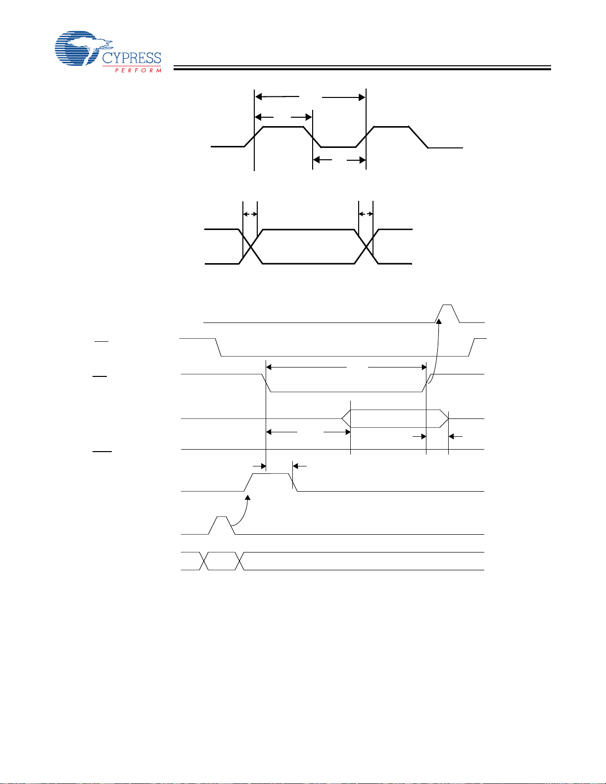
CY7C64013C
CY7C64113C
t
CYC
t
CH
CLOCK
t
CL
Figure 24-1. Clock Timing
D+
D−
Interrupt Generated
CS (P2.6, input)
OE (P2.5, input)
DATA (output)
(P2.4, input)
STB
DReadyPin (P2.3, output)
(Shown for DRDY Polarity=0)
t
r
OED
90%
t
RD
90%
10%
Figure 24-2. USB Data Signal Timing
t
t
OEDR
(Ready)
t
r
10%
D[23:0]
t
Int
OEZ
Internal Write
Internal Addr
Figure 24-3. HAPI Read by External Interface from USB Microcontroller
Document #: 38-08001 Rev. *B Page 47 of 51
Port0
[+] Feedback
Page 48

CY7C64013C
CY7C64113C
Interrupt Generated
CS
(P2.6, input)
STB
(P2.4, input)
DATA (input)
OE (P2.5, input)
LEmptyPin (P2.2, output)
(Shown for LEMPTY Polarity=0)
Internal Read
Internal Addr
Figure 24-4. HAPI Write by External Device to USB Microcontroller
t
STBLE
t
WR
D[23:0]
t
DSTB
(not empty)
t
STBZ
Int
Port0
25.0 Ordering Information
Ordering Code PROM Size Package Type
CY7C64013C-SXC 8 KB 28-Pin (300-Mil) SOIC Commercial
CY7C64013C-PXC 8 KB 28-Pin (300-Mil) PDIP Commercial
CY7C64013C-SXCT 8 KB 28-Pin (300-Mil) SOIC - Tape Reel Commercial
CY7C64113C-PVXC 8 KB 48-Pin (300-Mil) SSOP Commercial
Operating
Range
Document #: 38-08001 Rev. *B Page 48 of 51
[+] Feedback
Page 49

26.0 Package Diagrams
48-Lead Shrunk Small Outline Package
CY7C64013C
CY7C64113C
0.115[2.92]
0.160[4.06]
0.140[3.55]
0.190[4.82]
0.090[2.28]
0.110[2.79]
28-Lead (300-Mil) PDIP
SEE LEAD END OPTION
15 28
1.345[34.16]
1.385[35.18]
0.055[1.39]
0.065[1.65]
LEAD END OPTION
(LEAD #1, 14, 15 & 28)
0.015[0.38]
0.020[0.50]
51-85061-*C
114
0.260[6.60]
0.295[7.49]
0.030[0.76]
0.080[2.03]
SEATING PLANE
0.120[3.05]
0.140[3.55]
0.015[0.38]
0.060[1.52]
SEE LEAD END OPTION
DIMENSIONS IN INCHES [MM]
REFERENCE JEDEC MO-095
PACKAGE WEIGHT: 2.15 gms
0.290[7.36]
0.325[8.25]
0.009[0.23]
0.012[0.30]
0.310[7.87]
0.385[9.78]
MIN.
MAX.
3° MIN.
51-85014-*D
Document #: 38-08001 Rev. *B Page 49 of 51
[+] Feedback
Page 50

26.0 Package Diagrams (continued)
28-Lead (300-Mil) Molded SOIC
CY7C64013C
CY7C64113C
15 28
0.697[17.70]
0.713[18.11]
0.050[1.27]
TYP.
0.013[0.33]
0.019[0.48]
114
PIN1ID
0.291[7.39]
0.300[7.62]
0.026[0.66]
0.032[0.81]
0.092[2.33]
0.105[2.67]
0.004[0.10]
0.0118[0.30]
NOTE :
1. JEDEC STD REF MO-119
2. BODY LENGTH DIMENSION DOES NOT INCLUDE MOLD PROTRUSION/END FLASH,BUT
DOES INCLUDE MOLD MISMATCH AND ARE MEASURED AT THE MOLD PARTING LINE.
MOLD PROTRUSION/END FLASH SHALL NOT EXCEED 0.010 in (0.254 mm) PER SIDE
3. DIMENSIONS IN INCHES
4. PACKAGE WEIGHT 0.85gms
0.394[10.01]
0.419[10.64]
SEATING PLANE
*
*
0.004[0.10]
MIN.
MAX.
S28.3 STANDARD PKG.
SZ28.3 LEAD FREE PKG.
PART #
0.015[0.38]
0.050[1.27]
0.0091[0.23]
0.0125[3.17]
51-85026-*D
*
All product and company names mentioned in this document are the trademarks of their respective holders.
Document #: 38-08001 Rev. *B Page 50 of 51
© Cypress Semiconductor Corporation, 2006. The information contained herein is subject to change without notice. Cypress Semiconductor Corporation assumes no responsibility for the use
of any circuitry other than circuitry embodied in a Cypress product. Nor does it convey or imply any license under patent or other rights. Cypress products are not warranted nor intended to be
used for medical, life support, life saving, critical control or safety applications, unless pursuant to an express written agreement with Cypress. Furtherm ore, Cypress does not authori ze its
products for use as critical components in life-support systems where a malfunction or failure may reasonably be expected to result in significant injury to the user. The inclusion of Cypress
products in life-support systems application implies that the manufacturer assumes all risk of such use and in doing so indemnifies Cypress against all charges.
[+] Feedback
Page 51

CY7C64013C
CY7C64113C
Document History Page
Document Title: CY7C64013C, CY7C64113C Full-Speed USB (12 Mbps) Function
Document Number: 38-08001
REV. ECN NO.
** 109962 12/16/01 SZV Change from Spec number: 38-00626 to 38-08001
*A 129715 02/05/04 MON Added register bit definitions
*B 429099 See ECN TYJ Changed part numbers to the ‘C’ types. Included ‘Cypress Perform’ logo.
Issue
Date
Orig. of
Change Description of Change
Added default bit state of each register
Corrected the Schematic (location of the Pull up on D+)
Added register summary
Modified tables 19-1 and 19-2
Provided more explanation regarding locking/unlocking mechanism of the
mode register.
Updated part numbers in the Ordering section.
Document #: 38-08001 Rev. *B Page 51 of 51
[+] Feedback
 Loading...