


enCoRe USB™ CY7C63722/23
CY7C63743
CY7C63722/23
CY7C63743
enCoRe™ USB
Combination Low-Speed USB & PS/2
Peripheral Controller
Cypress Semiconductor Corporation • 3901 North First Street • San Jose, CA 95134 • 408-943-2600
Document #: 38-08022 Rev. ** Revised October 1, 2002

FOR
FOR
enCoRe™ USB CY7C63722/23
CY7C63743
TABLE OF CONTENTS
1.0 FEATURES ..................................................................................................................................... 5
2.0 FUNCTIONAL OVERVIEW .............................................................................................................6
2.1 enCoRe USB - The New USB Standard ....................................................................................6
3.0 LOGIC BLOCK DIAGRAM ............................................................................................................. 7
4.0 PIN CONFIGURATIONS .................................................................................................................7
5.0 PIN ASSIGNMENTS ....................................................................................................................... 7
6.0 PROGRAMMING MODEL ............................................................................................................... 8
6.1 Program Counter (PC) ...............................................................................................................8
6.2 8-bit Accumulator (A) ................................................................................................................. 8
6.3 8-bit Index Register (X) .............................................................................................................. 8
6.4 8-bit Program Stack Pointer (PSP) ............................................................................................ 8
6.5 8-bit Data Stack Pointer (DSP) .................................................................................................. 9
6.6 Address Modes ..........................................................................................................................9
6.6.1 Data ..................................................................................................................................................9
6.6.2 Direct ................................................................................................................................................ 9
6.6.3 Indexed ............................................................................................................................................ 9
7.0 INSTRUCTION SET SUMMARY ...................................................................................................10
8.0 MEMORY ORGANIZATION .......................................................................................................... 11
8.1 Program Memory Organization
................................................................................................ 11
8.2 Data Memory Organization ...................................................................................................... 12
8.3 I/O Register Summary .............................................................................................................13
9.0 CLOCKING .................................................................................................................................... 14
9.1 Internal/External Oscillator Operation ...................................................................................... 15
9.2 External Oscillator .................................................................................................................... 16
10.0 RESET ......................................................................................................................................... 16
10.1 Low-voltage Reset (LVR) .......................................................................................................16
10.2 Brown Out Reset (BOR) ........................................................................................................ 16
10.3 Watchdog Reset (WDR) ........................................................................................................17
11.0 SUSPEND MODE ........................................................................................................................17
11.1 Clocking Mode on Wake-up from Suspend ...........................................................................18
11.2 Wake-up Timer ...................................................................................................................... 18
12.0 GENERAL PURPOSE I/O PORTS ............................................................................................. 18
12.1 Auxiliary Input Port ................................................................................................................. 21
13.0 USB SERIAL INTERFACE ENGINE (SIE) ................................................................................. 22
13.1 USB Enumeration .................................................................................................................. 22
13.2 USB Port Status and Control .................................................................................................22
14.0 USB DEVICE ............................................................................................................................... 24
14.1 USB Address Register ........................................................................................................... 24
14.2 USB Control Endpoint ............................................................................................................24
14.3 USB Non-control Endpoints ................................................................................................... 25
14.4 USB Endpoint Counter Registers ..........................................................................................26
15.0 USB REGULATOR OUTPUT ......................................................................................................27
Document #: 38-08022 Rev. ** Page 2 of 58

FOR
FOR
enCoRe™ USB CY7C63722/23
CY7C63743
16.0 PS/2 OPERATION ....................................................................................................................... 27
17.0 SERIAL PERIPHERAL INTERFACE (SPI) ................................................................................. 28
17.1 Operation as an SPI Master ................................................................................................... 29
17.2 Master SCK Selection ............................................................................................................29
17.3 Operation as an SPI Slave .....................................................................................................29
17.4 SPI Status and Control ..........................................................................................................30
17.5 SPI Interrupt ........................................................................................................................... 31
17.6 SPI Modes for GPIO Pins ......................................................................................................31
18.0 12-BIT FREE-RUNNING TIMER .................................................................................................31
19.0 TIMER CAPTURE REGISTERS .................................................................................................32
20.0 PROCESSOR STATUS AND CONTROL REGISTER ...............................................................35
21.0 INTERRUPTS .............................................................................................................................. 36
21.1 Interrupt Vectors .................................................................................................................... 37
21.2 Interrupt Latency .................................................................................................................... 37
21.3 Interrupt Sources ...................................................................................................................37
22.0 USB MODE TABLES .................................................................................................................. 42
23.0 REGISTER SUMMARY ............................................................................................................... 47
24.0 ABSOLUTE MAXIMUM RATINGS ............................................................................................. 48
25.0 DC CHARACTERISTICS ............................................................................................................48
26.0 SWITCHING CHARACTERISTICS .............................................................................................50
27.0 ORDERING INFORMATION ....................................................................................................... 55
28.0 PACKAGE DIAGRAMS ..............................................................................................................55
LIST OF FIGURES
Figure 8-1. Program Memory Space with Interrupt Vector Table ........................................................ 11
Figure 8-2. Data Memory Organization ............................................................................................... 12
Figure 9-1. Clock Oscillator On-chip Circuit ......................................................................................... 14
Figure 9-2. Clock Configuration Register (Address 0xF8) ................................................................... 14
Figure 10-1. Watchdog Reset (WDR, Address 0x26) .......................................................................... 17
Figure 12-1. Block Diagram of GPIO Port (one pin shown) ................................................................. 19
Figure 12-2. Port 0 Data (Address 0x00) ............................................................................................. 19
Figure 12-3. Port 1 Data (Address 0x01) ............................................................................................. 19
Figure 12-4. GPIO Port 0 Mode0 Register (Address 0x0A) ................................................................. 20
Figure 12-5. GPIO Port 0 Mode1 Register (Address 0x0B) ................................................................. 20
Figure 12-6. GPIO Port 1 Mode0 Register (Address 0x0C) ................................................................ 20
Figure 12-7. GPIO Port 1 Mode1 Register (Address 0x0D) ................................................................ 20
Figure 12-8. Port 2 Data Register (Address 0x02) ..............................................................................21
Figure 13-1. USB Status and Control Register (Address 0x1F) .......................................................... 23
Figure 14-1. USB Device Address Register (Address 0x10) ............................................................... 24
Figure 14-2. Endpoint 0 Mode Register (Address 0x12) ..................................................................... 25
Figure 14-3. USB Endpoint EP1, EP2 Mode Registers (Addresses 0x14 and 0x16) .......................... 26
Figure 14-4. Endpoint 0,1,2 Counter Registers (Addresses 0x11, 0x13 and 0x15) ............................26
Figure 17-1. SPI Block Diagram .......................................................................................................... 28
Figure 16-1. Diagram of USB-PS/2 System Connections ................................................................... 28
Figure 17-2. SPI Data Register (Address 0x60) .................................................................................. 29
Figure 17-3. SPI Control Register (Address 0x61) ..............................................................................30
Document #: 38-08022 Rev. ** Page 3 of 58

FOR
FOR
enCoRe™ USB CY7C63722/23
CY7C63743
Figure 17-4. SPI Data Timing .............................................................................................................. 31
Figure 18-1. Timer LSB Register (Address 0x24) ................................................................................31
Figure 18-2. Timer MSB Register (Address 0x25) ............................................................................... 32
Figure 18-3. Timer Block Diagram ....................................................................................................... 32
Figure 19-1. Capture Timers Block Diagram ....................................................................................... 33
Figure 19-2. Capture Timer A-Rising, Data Register (Address 0x40) ................................................. 33
Figure 19-3. Capture Timer A-Falling, Data Register (Address 0x41) ................................................. 34
Figure 19-4. Capture Timer B-Rising, Data Register (Address 0x42) ................................................. 34
Figure 19-5. Capture Timer B-Falling, Data Register (Address 0x43) ................................................. 34
Figure 19-6. Capture Timer Status Register (Address 0x45) .............................................................. 34
Figure 19-7. Capture Timer Configuration Register (Address 0x44) ................................................... 34
Figure 20-1. Processor Status and Control Register (Address 0xFF) ................................................. 35
Figure 21-1. Global Interrupt Enable Register (Address 0x20) ............................................................ 38
Figure 21-2. Endpoint Interrupt Enable Register (Address 0x21) ........................................................ 39
Figure 21-3. Interrupt Controller Logic Block Diagram ........................................................................40
Figure 21-4. Port 0 Interrupt Enable Register (Address 0x04) ............................................................ 40
Figure 21-5. Port 1 Interrupt Enable Register (Address 0x05) ............................................................ 40
Figure 21-6. Port 0 Interrupt Polarity Register (Address 0x06) ............................................................ 41
Figure 21-7. Port 1 Interrupt Polarity Register (Address 0x07) ............................................................ 41
Figure 21-8. GPIO Interrupt Diagram .................................................................................................. 41
Figure 26-1. Clock Timing .................................................................................................................... 51
Figure 26-2. USB Data Signal Timing ..................................................................................................51
Figure 26-3. Receiver Jitter Tolerance ................................................................................................ 52
Figure 26-4. Differential to EOP Transition Skew and EOP Width ...................................................... 52
Figure 26-5. Differential Data Jitter ...................................................................................................... 52
Figure 26-7. SPI Slave Timing, CPHA = 0 ........................................................................................... 53
Figure 26-6. SPI Master Timing, CPHA = 0 ......................................................................................... 53
Figure 26-8. SPI Master Timing, CPHA = 1 ......................................................................................... 54
Figure 26-9. SPI Slave Timing, CPHA = 1 ........................................................................................... 54
LIST OF TABLES
Table 8-1. I/O Register Summary ........................................................................................................13
Table 11-1. Wake-up Timer Adjust Settings ........................................................................................ 18
Table 12-1. Ports 0 and 1 Output Control Truth Table ........................................................................21
Table 13-1. Control Modes to Force D+/D– Outputs ........................................................................... 24
Table 17-1. SPI Pin Assignments ........................................................................................................31
Table 19-1. Capture Timer Prescalar Settings (Step size and range for FCLK = 6 MHz) ...................35
Table 21-1. Interrupt Vector Assignments ...........................................................................................37
Table 22-1. USB Register Mode Encoding for Control and Non-Control Endpoints ............................42
Table 22-2. Decode table for Table 22-3: “Details of Modes for Differing Traffic Conditions” .............44
Table 22-3. Details of Modes for Differing Traffic Conditions ..............................................................45
Table 28-1. CY7C63722-XC Probe Pad Coordinates in microns ((0,0) to bond pad centers) ............57
Document #: 38-08022 Rev. ** Page 4 of 58

FOR
FOR
enCoRe™ USB CY7C63722/23
CY7C63743
1.0 Features
• enCoRe™ USB - enhanced Component Reduction
— Internal oscillator eliminates the need for an external crystal or resonator
— Interface can auto-configure to operate as PS/2 or USB without the need for external components to switch between
modes (no GPIO pins needed to manage dual mode capability)
— Internal 3.3V regulator for USB pull-up resistor
— Configurable GPIO for real-world interface without external components
• Flexible, cost-effective solution for applications that combine PS/2 and low-speed USB, such as mice, gamepads,
joysticks, and many others.
• USB Specification Compliance
— Conforms to USB Specification, Version 2.0
— Conforms to USB HID Specification, Version 1.1
— Supports 1 Low-Speed USB device address and 3 data endpoints
— Integrated USB transceiver
— 3.3V regulated output for USB pull-up resistor
• 8-bit RISC microcontroller
— Harvard architecture
— 6-MHz external ceramic resonator or internal clock mode
— 12-MHz internal CPU clock
— Internal memory
— 256 bytes of RAM
— 8 Kbytes of EPROM
— Interface can auto-configure to operate as PS/2 or USB
— No external components for switching between PS/2 and USB modes
— No GPIO pins needed to manage dual mode capability
•I/O ports
— Up to 16 versatile General Purpose I/O (GPIO) pins, individually configurable
— High current drive on any GPIO pin: 50 mA/pin current sink
— Each GPIO pin supports high-impedance inputs, internal pull-ups, open drain outputs or traditional CMOS outputs
— Maskable interrupts on all I/O pins
• SPI serial communication block
— Master or slave operation
— 2 Mbit/s transfers
• Four 8-bit Input Capture registers
— Two registers each for two input pins
— Capture timer setting with 5 prescaler settings
— Separate registers for rising and falling edge capture
— Simplifies interface to RF inputs for wireless applications
• Internal low-power wake-up timer during suspend mode
— Periodic wake-up with no external components
• Optional 6-MHz internal oscillator mode
— Allows fast start-up from suspend mode
• Watchdog Reset (WDR)
• Low-voltage Reset at 3.75V
• Internal brown-out reset for suspend mode
• Improved output drivers to reduce EMI
• Operating voltage from 4.0V to 5.5VDC
• Operating temperature from 0 to 70 degrees Celsius
• CY7C63723 available in 18-pin SOIC, 18-pin PDIP
• CY7C63743 available in 24-pin SOIC, 24-pin PDIP
• CY7C63722 available in DIE form
• Industry standard programmer support
Document #: 38-08022 Rev. ** Page 5 of 58

FOR
FOR
enCoRe™ USB CY7C63722/23
CY7C63743
2.0 Functional Overview
2.1 enCoRe USB - The New USB Standard
Cypress has re-invented its leadership position in the low-speed USB market with a new family of innovative microcontrollers.
Introducing...enCoRe USB—“enhanced Component Reduction.” Cypress has leveraged its design expertise in USB solutions to
create a new family of low-speed USB microcontrollers that enables peripheral developers to design new products with a minimum
number of components. At the heart of the enCoRe USB technology is the breakthrough design of a crystal-less oscillator. By
integrating the oscillator into our chip, an external crystal or resonator is no longer needed. We have also integrated other external
components commonly found in low-speed USB applications such as pull-up resistors, wake-up circuitry, and a 3.3V regulator.
All of this adds up to a lower system cost.
The CY7C637xx is an 8-bit RISC One Time Programmable (OTP) microcontroller. The instruction set has been optimized specifically for USB and PS/2 operations, although the microcontrollers can be used for a variety of other embedded applications.
The CY7C637xx features up to 16 general purpose I/O (GPIO) pins to support USB, PS/2 and other applications. The I/O pins
are grouped into two ports (Port 0 to 1) where each pin can be individually configured as inputs with internal pull-ups, open drain
outputs, or traditional CMOS outputs with programmable drive strength of up to 50 mA output drive. Additionally, each I/O pin can
be used to generate a GPIO interrupt to the microcontroller. Note the GPIO interrupts all share the same “GPIO” interrupt vector.
The CY7C637xx microcontrollers feature an internal oscillator. With the presence of USB traffic, the internal oscillator can be set
to precisely tune to USB timing requirements (6 MHz ±1.5%). Optionally, an external 6-MHz ceramic resonator can be used to
provide a higher precision reference for USB operation. This clock generator reduces the clock-related noise emissions (EMI).
The clock generator provides the 6- and 12-MHz clocks that remain internal to the microcontroller.
The CY7C637xx has 8 Kbytes of EPROM and 256 bytes of data RAM for stack space, user variables, and USB FIFOs.
These parts include low-voltage reset logic, a watchdog timer, a vectored interrupt controller, a 12-bit free-running timer, and
capture timers. The low-voltage reset (LVR) logic detects when power is applied to the device, resets the logic to a known state,
and begins executing instructions at EPROM address 0x0000. LVR will also reset the part when V
voltage range. The watchdog timer can be used to ensure the firmware never gets stalled for more than approximately 8 ms.
The microcontroller supports 10 maskable interrupts in the vectored interrupt controller. Interrupt sources include the USB
Bus-Reset, the 128-µs and 1.024-ms outputs from the free-running timer, three USB endpoints, two capture timers, an internal
wake-up timer and the GPIO ports. The timers bits cause periodic interrupts when enabled. The USB endpoints interrupt after
USB transactions complete on the bus. The capture timers interrupt whenever a new timer value is saved due to a selected GPIO
edge event. The GPIO ports have a level of masking to select which GPIO inputs can cause a GPIO interrupt. For additional
flexibility, the input transition polarity that causes an interrupt is programmable for each GPIO pin. The interrupt polarity can be
either rising or falling edge.
The free-running 12-bit timer clocked at 1 MHz provides two interrupt sources as noted above (128 µs and 1.024 ms). The timer
can be used to measure the duration of an event under firmware control by reading the timer at the start and end of an event,
and subtracting the two values. The four capture timers save a programmable 8 bit range of the free-running timer when a GPIO
edge occurs on the two capture pins (P0.0, P0.1).
The CY7C637xx includes an integrated USB serial interface engine (SIE) that supports the integrated peripherals. The hardware
supports one USB device address with three endpoints. The SIE allows the USB host to communicate with the function integrated
into the microcontroller. A 3.3V regulated output pin provides a pull-up source for the external USB resistor on the D– pin.
The USB D+ and D– USB pins can alternately be used as PS/2 SCLK and SDATA signals, so that products can be designed to
respond to either USB or PS/2 modes of operation. PS/2 operation is supported with internal pull-up resistors on SCLK and
SDATA, the ability to disable the regulator output pin, and an interrupt to signal the start of PS/2 activity. No external components
are necessary for dual USB and PS/2 systems, and no GPIO pins need to be dedicated to switching between modes. Slow edge
rates operate in both modes to reduce EMI.
drops below the operating
CC
Document #: 38-08022 Rev. ** Page 6 of 58
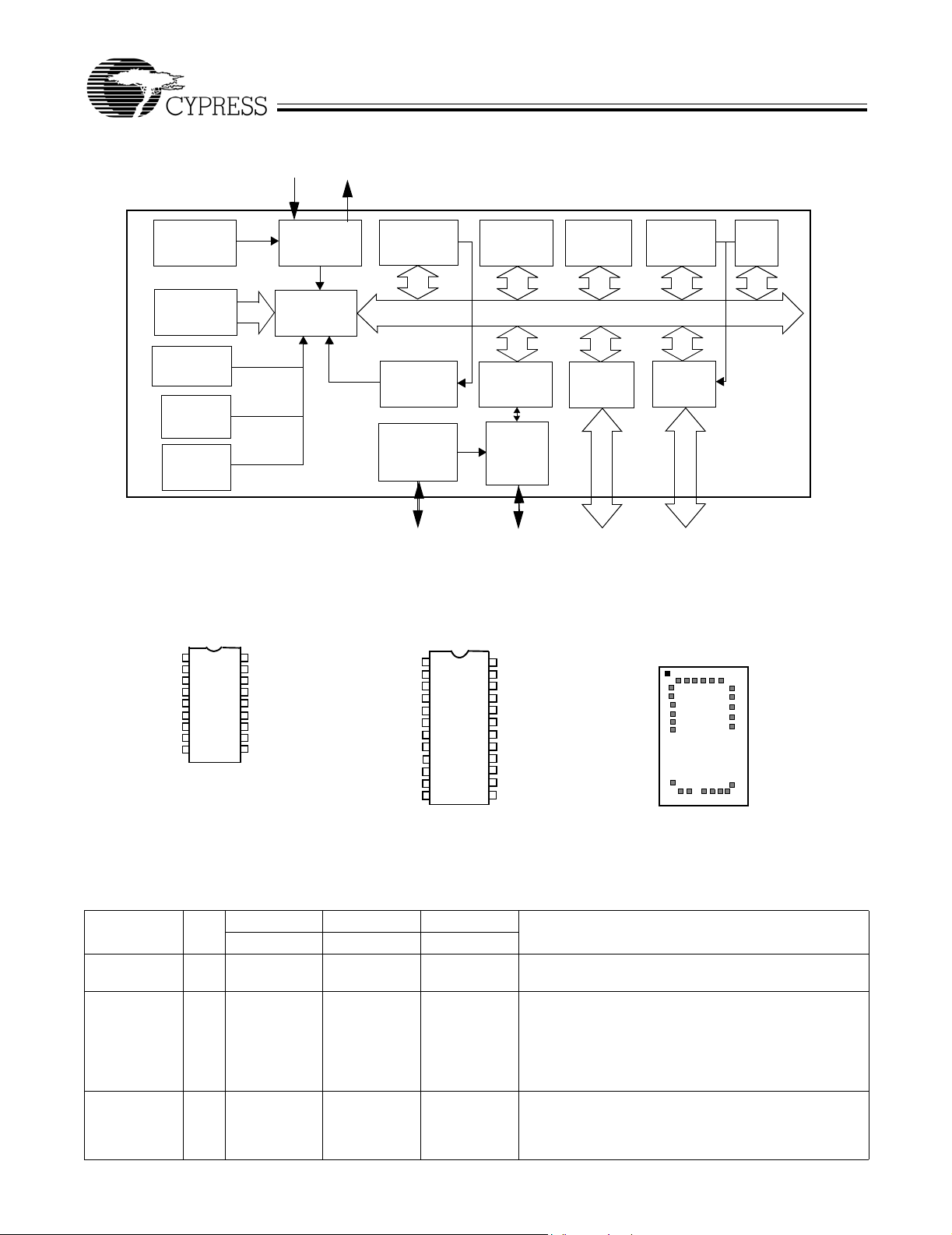
3.0 Logic Block Diagram
FOR
FOR
enCoRe™ USB CY7C63722/23
CY7C63743
XTALOUT XTALIN/P2.1
Internal
Oscillator
EPROM
8K Byte
Brown-out
Reset
Watch
Dog
Timer
Low
Voltage
Reset
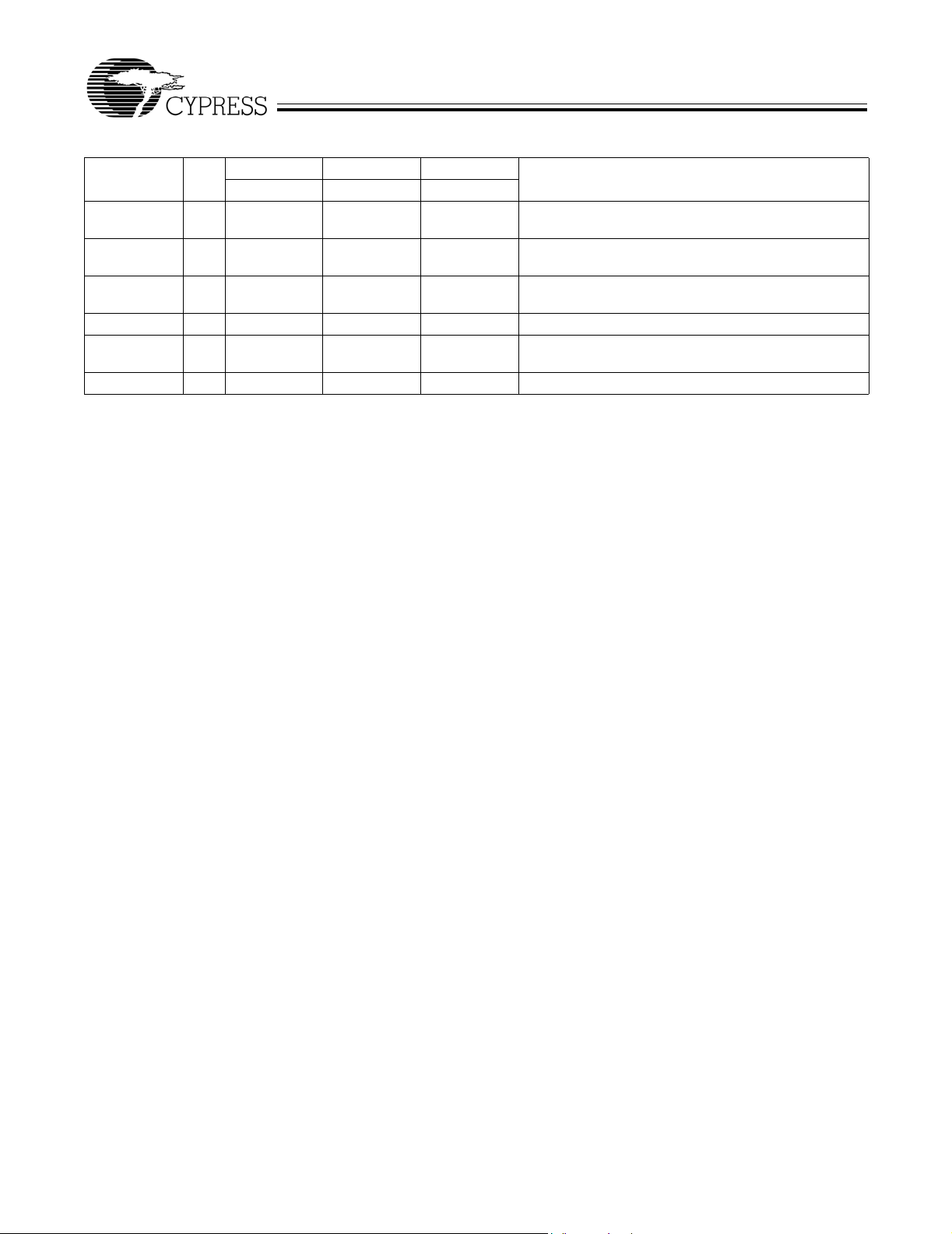
4.0 Pin Configurations
CY7C63723
18-pin SOIC/PDIP
P0.0
P0.1
P0.2
P0.3
VSS
VPP
VREG/P2.0
XTALIN/P2.1
1
2
3
4
5
6
7
8
9
18
17
16
15
14P1.0
13
12
11
10
P0.4
P0.5
P0.6
P0.7
P1.1
D+/SCLK
D–/SDATA
VCC
XTALOUT
Xtal
Oscillator
8-bit
RISC
Core
Wake-Up
Timer
Interrupt
Controller
3.3V
Regulator
VREG/P2.0
CY7C63743
24-pin SOIC/PDIP
P0.0
P0.1
P0.2
P0.3
P1.0
P1.2
P1.4
P1.6
VSS
VPP
VREG/P2.0
XTALIN/P2.1
Top View
1
2
3
4
5
6
7
8
9
10
11
12
RAM
256 Byte
USB
Engine
USB &
PS/2
Xcvr
D+,D–
P0.4
24
23
P0.5
P0.6
22
21
P0.7
P1.1
20
P1.3
19
18
P1.5
17
P1.7
16
D+/SCLK
D–/SDATA
15
VCC
14
XTALOUT
13
12-bit
Timer
Port 1
GPIO
P1.0–P1.7
Capture
Timers
Port 0
GPIO
P0.0–P0.7
CY7C63722-XC
3 P0.2
2 P0.1
P0.3
4
P1.0
5
6
P1.2
P1.4
7
P1.6
8
9
VSS
VSS
10
111213
VPP
VREG
DIE
1 P0.0
25 P0.4
SPI
24 P0.5
23 P0.6
P0.7
22
P1.1
21
20
P1.3
19
P1.5
18
P1.7
17
D+/SCLK
15
16
14
VCC
D-/SDATA
XTALOUT
XTALIN/P2.1
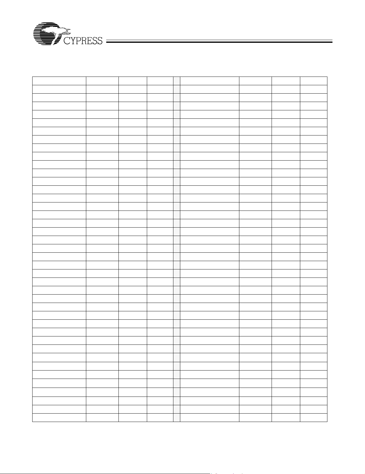
5.0 Pin Assignments
CY7C63723 CY7C63743 CY7C63722
Name I/O
D–/SDATA,
D+/SCLK
P0[7:0] I/O 1, 2, 3, 4,
I/O 12
13
15, 16, 17, 18
15
16
1, 2, 3, 4,
21, 22, 23, 24
16
17
1, 2, 3, 4,
22, 23, 24, 25
USB differential data lines (D– and D+), or PS/2 clock
and data signals (SDATA and SCLK)
GPIO Port 0 capable of sinking up to 50 mA/pin, or
sinking controlled low or high programmable current.
Can also source 2 mA current, provide a resistive
pull-up, or serve as a high-impedance input. P0.0 and
P0.1 provide inputs to Capture Timers A and B, respectively.
P1[7:0] I/O 5, 14 5, 6, 7, 8,
17, 18, 19, 20
5, 6, 7, 8,
18, 19, 20, 21
IO Port 1 capable of sinking up to 50 mA/pin, or sinking
controlled low or high programmable current. Can also
source 2 mA current, provide a resistive pull-up, or
serve as a high-impedance input.
Document #: 38-08022 Rev. ** Page 7 of 58
Description18-Pin 24-Pin 25-Pad
FOR
FOR
enCoRe™ USB CY7C63722/23
CY7C63743
5.0 Pin Assignments (continued)
CY7C63723 CY7C63743 CY7C63722
Name I/O
XTALIN/P2.1 IN 9 12 13 6-MHz ceramic resonator or external clock input, or
XTALOUT OUT 10 13 14 6-MHz ceramic resonator return pin or internal oscillator
V
PP
V
CC
VREG/P2.0 8 11 12 Voltage supply for 1.3-kΩ USB pull-up resistor (3.3V
V
SS
7 10 11 Programming voltage supply, ground for normal
11 14 15 Voltage supply
6 9 9, 10 Ground
P2.1 input
output
operation
nominal). Also serves as P2.0 input.
6.0 Programming Model
Refer to the CYASM Assembler User’s Guide for more details on firmware operation with the CY7C637xx microcontrollers.
Description18-Pin 24-Pin 25-Pad
6.1 Program Counter (PC)
The 14-bit program counter (PC) allows access for up to 8 Kbytes of EPROM using the CY7C637xx architecture. The program
counter is cleared during reset, such that the first instruction executed after a reset is at address 0x0000. This instruction is
typically a jump instruction to a reset handler that initializes the application.
The lower 8 bits of the program counter are incremented as instructions are loaded and executed. The upper 6 bits of the program
counter are incremented by executing an XPAGE instruction. As a result, the last instruction executed within a 256-byte “page”
of sequential code should be an XPAGE instruction. The assembler directive “XPAGEON” will cause the assembler to insert
XPAGE instructions automatically. As instructions can be either one or two bytes long, the assembler may occasionally need to
insert a NOP followed by an XPAGE for correct execution.
The program counter of the next instruction to be executed, carry flag, and zero flag are saved as two bytes on the program stack
during an interrupt acknowledge or a CALL instruction. The program counter, carry flag, and zero flag are restored from the
program stack only during a RETI instruction.
Please note the program counter cannot be accessed directly by the firmware. The program stack can be examined by reading
SRAM from location 0x00 and up.
6.2 8-bit Accumulator (A)
The accumulator is the general-purpose, do everything register in the architecture where results are usually calculated.
6.3 8-bit Index Register (X)
The index register “X” is available to the firmware as an auxiliary accumulator. The X register also allows the processor to perform
indexed operations by loading an index value into X.
6.4 8-bit Program Stack Pointer (PSP)
During a reset, the program stack pointer (PSP) is set to zero. This means the program “stack” starts at RAM address 0x00 and
“grows” upward from there. Note that the program stack pointer is directly addressable under firmware control, using the MOV
PSP,A instruction. The PSP supports interrupt service under hardware control and CALL, RET, and RETI instructions under
firmware control.
During an interrupt acknowledge, interrupts are disabled and the program counter, carry flag, and zero flag are written as two
bytes of data memory. The first byte is stored in the memory addressed by the program stack pointer, then the PSP is incremented.
The second byte is stored in memory addressed by the program stack pointer and the PSP is incremented again. The net effect
is to store the program counter and flags on the program “stack” and increment the program stack pointer by two.
The return from interrupt (RETI) instruction decrements the program stack pointer, then restores the second byte from memory
addressed by the PSP. The program stack pointer is decremented again and the first byte is restored from memory addressed
by the PSP. After the program counter and flags have been restored from stack, the interrupts are enabled. The effect is to restore
the program counter and flags from the program stack, decrement the program stack pointer by two, and re-enable interrupts.
The call subroutine (CALL) instruction stores the program counter and flags on the program stack and increments the PSP by two.
Document #: 38-08022 Rev. ** Page 8 of 58

FOR
FOR
enCoRe™ USB CY7C63722/23
CY7C63743
The return from subroutine (RET) instruction restores the program counter, but not the flags, from program stack and decrements
the PSP by two.
Note that there are restrictions in using the JMP, CALL, and INDEX instructions across the 4-KB boundary of the program memory.
Refer to the CYASM Assembler User’s Guide for a detailed description.
6.5 8-bit Data Stack Pointer (DSP)
The data stack pointer (DSP) supports PUSH and POP instructions that use the data stack for temporary storage. A PUSH
instruction will pre-decrement the DSP, then write data to the memory location addressed by the DSP. A POP instruction will read
data from the memory location addressed by the DSP, then post-increment the DSP.
During a reset, the Data Stack Pointer will be set to zero. A PUSH instruction when DSP equals zero will write data at the top of
the data RAM (address 0xFF). This would write data to the memory area reserved for a FIFO for USB endpoint 0. In non-USB
applications, this works fine and is not a problem.
For USB applications, the firmware should set the DSP to an appropriate location to avoid a memory conflict with RAM dedicated
to USB FIFOs. The memory requirements for the USB endpoints are shown in Section 8.2. For example, assembly instructions
to set the DSP to 20h (giving 32 bytes for program and data stack combined) are shown below:
MOV A,20h ; Move 20 hex into Accumulator (must be D8h or less to avoid USB FIFOs)
SWAP A,DSP ; swap accumulator value into DSP register
6.6 Address Modes
The CY7C637xx microcontrollers support three addressing modes for instructions that require data operands: data, direct, and
indexed.
6.6.1 Data
The “Data” address mode refers to a data operand that is actually a constant encoded in the instruction. As an example, consider
the instruction that loads A with the constant 0x30:
• MOV A, 30h
This instruction will require two bytes of code where the first byte identifies the “MOV A” instruction with a data operand as the
second byte. The second byte of the instruction will be the constant “0xE8h”. A constant may be referred to by name if a prior
“EQU” statement assigns the constant value to the name. For example, the following code is equivalent to the example shown
above:
• DSPINIT: EQU 30h
• MOV A,DSPINIT
6.6.2 Direct
“Direct” address mode is used when the data operand is a variable stored in SRAM. In that case, the one byte address of the
variable is encoded in the instruction. As an example, consider an instruction that loads A with the contents of memory address
location 0x10h:
• MOV A, [10h]
In normal usage, variable names are assigned to variable addresses using “EQU” statements to improve the readability of the
assembler source code. As an example, the following code is equivalent to the example shown above:
• buttons: EQU 10h
• MOV A,[buttons]
6.6.3 Indexed
“Indexed” address mode allows the firmware to manipulate arrays of data stored in SRAM. The address of the data operand is
the sum of a constant encoded in the instruction and the contents of the “X” register. In normal usage, the constant will be the
“base” address of an array of data and the X register will contain an index that indicates which element of the array is actually
addressed:
• array: EQU 10h
•MOV X,3
• MOV A,[x+array]
This would have the effect of loading A with the fourth element of the SRAM “array” that begins at address 0x10h. The fourth
element would be at address 0x13h.
Document #: 38-08022 Rev. ** Page 9 of 58
FOR
FOR
enCoRe™ USB CY7C63722/23
CY7C63743
7.0 Instruction Set Summary
Refer to the CYASM Assembler User’s Guide for detailed information on these instructions. Note that conditional jump instructions
(i.e., JC, JNC, JZ, JNZ) take 5 cycles if jump is taken, 4 cycles if no jump.
MNEMONIC Operand Opcode Cycles
HALT 00 7
ADD A,expr data 01 4
ADD A,[expr] direct 02 6 INC X x 22 4
ADD A,[X+expr] index 03 7
ADC A,expr data 04 4
ADC A,[expr] direct 05 6 DEC A acc 25 4
ADC A,[X+expr] index 06 7 DEC X x 26 4
SUB A,expr data 07 4
SUB A,[expr] direct 08 6 DEC [X+expr] index 28 8
SUB A,[X+expr] index 09 7
SBB A,expr data 0A 4
SBB A,[expr] direct 0B 6 POP A 2B 4
SBB A,[X+expr] index 0C 7 POP X 2C 4
OR A,expr data 0D 4
OR A,[expr] direct 0E 6 PUSH X 2E 5
OR A,[X+expr] index 0F 7 SWAP A,X 2F 5
AND A,expr data 10 4
AND A,[expr] direct 11 6 MOV [expr],A direct 31 5
AND A,[X+expr] index 12 7 MOV [X+expr],A index 32 6
XOR A,expr data 13 4
XOR A,[expr] direct 14 6 OR [X+expr],A index 34 8
XOR A,[X+expr] index 15 7 AND [expr],A direct 35 7
CMP A,expr data 16 5
CMP A,[expr] direct 17 7 XOR [expr],A direct 37 7
CMP A,[X+expr] index 18 8 XOR [X+expr],A index 38 8
MOV A,expr data 19 4
MOV A,[expr] direct 1A 5 CPL 3A 4
MOV A,[X+expr] index 1B 6
MOV X,expr data 1C 4
MOV X,[expr] direct 1D 5
reserved 1E
XPAGE 1F 4
MOV A,X 40 4
MOV X,A 41 4
MOV PSP,A 60 4
CALL addr 50 - 5F 10
JMP addr 80-8F 5
CALL addr 90-9F 10
JZ addr A0-AF 5 (or 4) JACC addr E0-EF 7
JNZ addr B0-BF 5 (or 4)
MNEMONIC Operand Opcode Cycles
NOP 20 4
INC A acc 21 4
INC [expr] direct 23 7
INC [X+expr] index 24 8
DEC [expr] direct 27 7
IORD expr address 29 5
IOWR expr address 2A 5
PUSH A 2D 5
SWAP A,DSP 30 5
OR [expr],A direct 33 7
AND [X+expr],A index 36 8
IOWX [X+expr] index 39 6
ASL 3B 4
ASR 3C 4
RLC 3D 4
RRC 3E 4
RET 3F 8
DI 70 4
EI 72 4
RETI 73 8
JC addr C0-CF 5 (or 4)
JNC addr D0-DF 5 (or 4)
INDEX addr F0-FF 14
Document #: 38-08022 Rev. ** Page 10 of 58
8.0 Memory Organization
FOR
FOR
enCoRe™ USB CY7C63722/23
CY7C63743
8.1 Program Memory Organization
After reset Address
14 -bit PC 0x0000 Program execution begins here after a reset.
[1]
0x0002 USB Bus Reset interrupt vector
0x0004 128-µs timer interrupt vector
0x0006 1.024-ms timer interrupt vector
0x0008 USB endpoint 0 interrupt vector
0x000A USB endpoint 1 interrupt vector
0x000C USB endpoint 2 interrupt vector
0x000E SPI interrupt vector
0x0010 Capture timer A interrupt Vector
0x0012 Capture timer B interrupt vector
0x0014 GPIO interrupt vector
0x0016 Wake-up interrupt vector
0x0018 Program Memory begins here
0x1FDF 8 KB PROM ends here (8K - 32 bytes). See Note below
Figure 8-1. Program Memory Space with Interrupt Vector Table
Note:
1. The upper 32 bytes of the 8K PROM are reserved. Therefore, the user’s program must not overwrite this space.
Document #: 38-08022 Rev. ** Page 11 of 58
FOR
FOR
enCoRe™ USB CY7C63722/23
CY7C63743
8.2 Data Memory Organization
The CY7C637xx microcontrollers provide 256 bytes of data RAM. In normal usage, the SRAM is partitioned into four areas:
program stack, data stack, user variables and USB endpoint FIFOs as shown below:
After reset Address
8-bit DSP 8-bit PSP 0x00 Program Stack Growth
(User’s firmware moves
DSP)
8-bit DSP User Selected Data Stack Growth
User Variables
0xE8
USB FIFO for Address A endpoint 2
0xF0
0xF8
Top of RAM Memory 0xFF
Figure 8-2. Data Memory Organization
USB FIFO for Address A endpoint 1
USB FIFO for Address A endpoint 0
Document #: 38-08022 Rev. ** Page 12 of 58
FOR
FOR
enCoRe™ USB CY7C63722/23
CY7C63743
8.3 I/O Register Summary
I/O registers are accessed via the I/O Read (IORD) and I/O Write (IOWR, IOWX) instructions. IORD reads the selected port into
the accumulator. IOWR writes data from the accumulator to the selected port. Indexed I/O Write (IOWX) adds the contents of X
to the address in the instruction to form the port address and writes data from the accumulator to the specified port. Note that
specifying address 0 with IOWX (e.g., IOWX 0h) means the I/O port is selected solely by the contents of X.
Note: All bits of all registers are cleared to all zeros on reset, except the Processor Status and Control Register (Figure 20-1).
All registers not listed are reserved, and should never be written by firmware. All bits marked as reserved should always be written
as 0 and be treated as undefined by reads.
Table 8-1. I/O Register Summary
Register Name I/O Address Read/Write Function Fig.
Port 0 Data 0x00 R/W GPIO Port 0 12-2
Port 1 Data 0x01 R/W GPIO Port 1 12-3
Port 2 Data 0x02 R Auxiliary input register for D+, D–, VREG, XTALIN 12-8
Port 0 Interrupt Enable 0x04 W Interrupt enable for pins in Port 0 21-4
Port 1 Interrupt Enable 0x05 W Interrupt enable for pins in Port 1 21-5
Port 0 Interrupt Polarity 0x06 W Interrupt polarity for pins in Port 0 21-6
Port 1 Interrupt Polarity 0x07 W Interrupt polarity for pins in Port 1 21-7
Port 0 Mode0 0x0A W Controls output configuration for Port 0 12-4
Port 0 Mode1 0x0B W 12-5
Port 1 Mode0 0x0C W Controls output configuration for Port 1 12-6
Port 1 Mode1 0x0D W 12-7
USB Device Address 0x10 R/W USB Device Address register 14-1
EP0 Counter Register 0x11 R/W USB Endpoint 0 counter register 14-4
EP0 Mode Register 0x12 R/W USB Endpoint 0 configuration register 14-2
EP1 Counter Register 0x13 R/W USB Endpoint 1 counter register 14-4
EP1 Mode Register 0x14 R/W USB Endpoint 1 configuration register 14-3
EP2 Counter Register 0x15 R/W USB Endpoint 2 counter register 14-4
EP2 Mode Register 0x16 R/W USB Endpoint 2 configuration register 14-3
USB Status & Control 0x1F R/W USB status and control register 13-1
Global Interrupt Enable 0x20 R/W Global interrupt enable register 21-1
Endpoint Interrupt Enable 0x21 R/W USB endpoint interrupt enables 21-2
Timer (LSB) 0x24 R Lower 8 bits of free-running timer (1 MHz) 18-1
Timer (MSB) 0x25 R Upper 4 bits of free-running timer 18-2
WDR Clear 0x26 W Watchdog Reset clear -
Capture Timer A Rising 0x40 R Rising edge Capture Timer A data register 19-2
Capture Timer A Falling 0x41 R Falling edge Capture Timer A data register 19-3
Capture Timer B Rising 0x42 R Rising edge Capture Timer B data register 19-4
Capture Timer B Falling 0x43 R Falling edge Capture Timer B data register 19-5
Capture TImer Configuration 0x44 R/W Capture Timer configuration register 19-7
Capture Timer Status 0x45 R Capture Timer status register 19-6
SPI Data 0x60 R/W SPI read and write data register 17-2
SPI Control 0x61 R/W SPI status and control register 17-3
Clock Configuration 0xF8 R/W Internal / External Clock configuration register 9-2
Processor Status & Control 0xFF R/W Processor status and control 20-1
Document #: 38-08022 Rev. ** Page 13 of 58
FOR
FOR
enCoRe™ USB CY7C63722/23
CY7C63743
9.0 Clocking
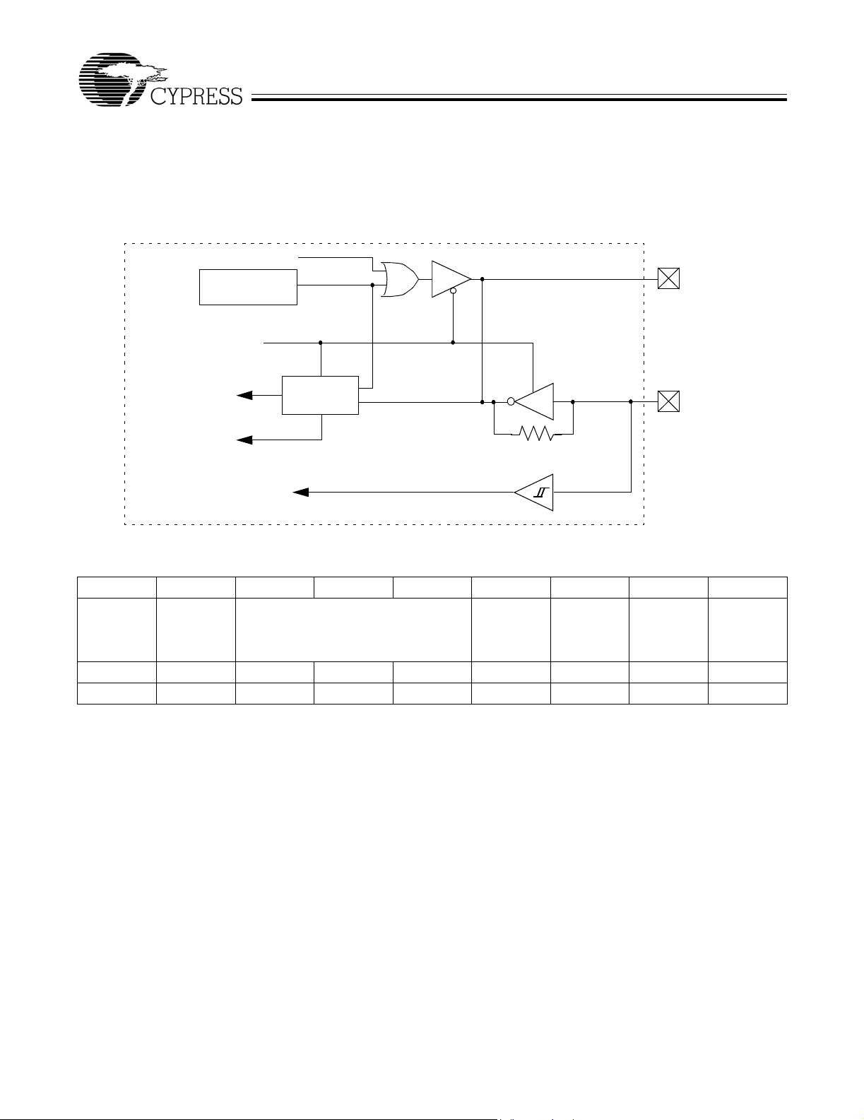
The chip can be clocked from either the internal on-chip clock, or from an oscillator based on an external resonator/crystal, as
shown in Figure 9-1. No additional capacitance is included on chip at the XTALIN/OUT pins. Operation is controlled by the Clock
Configuration Register, Figure 9-2.
Int Clk Output Disable
Internal Osc
Ext Clk Enable
XTALOUT
Clk2x (12 MHz)
(to Microcontroller)
Clk1x (6 MHz)
(to USB SIE)
Port 2.1
Bit # 76543210
Bit Name Ext. Clock
Resume
Delay
Read/Write R/W R/W R/W R/W R/W R/W R/W R/W
Reset 00000000
Bit 7: Ext. Clock Resume Delay
External Clock Resume Delay bit selects the delay time when switching to the external oscillator from the internal oscillator
mode, or when waking from suspend mode with the external oscillator enabled.
1 = 4 ms delay.
0 = 128 µs delay.
The delay gives the oscillator time to start up. The shorter time is adequate for operation with ceramic resonators, while the
longer time is preferred for start-up with a crystal. (These times do not include an initial oscillator start-up time which depends
on the resonating element. This time is typically 50–100 µs for ceramic resonators and 1–10 ms for crystals). Note that this
bit only selects the delay time for the external clock mode. When waking from suspend mode with the internal oscillator (Bit 0
is LOW), the delay time is only 8 µs in addition to a delay of approximately 1 µs for the oscillator to start.
Bit [6:4]: Wake-up Timer Adjust Bit [2:0]
The Wake-up Timer Adjust Bits are used to adjust the Wake-up timer period.
If the Wake-up interrupt is enabled in the Global Interrupt Enable Register, the microcontroller will generate wake-up interrupts
periodically. The frequency of these periodical wake-up interrupts is adjusted by setting the Wake-up Timer Adjust Bit [2:0],
as described in Section 11.2. One common use of the wake-up interrupts is to generate periodical wake-up events during
suspend mode to check for changes, such as looking for movement in a mouse, while maintaining a low average power.
Clock
Doubler
Figure 9-1. Clock Oscillator On-chip Circuit
Wake-up Timer Adjust Bit [2:0] Low-voltage
Reset
Disable
Figure 9-2. Clock Configuration Register (Address 0xF8)
Precision
USB
Clocking
Enable
Internal
Clock
Output
Disable
XTALIN
External
Oscillator
Enable
Document #: 38-08022 Rev. ** Page 14 of 58

FOR
FOR
enCoRe™ USB CY7C63722/23
CY7C63743
Bit 3: Low-voltage Reset Disable
When V
microcontroller enters a partial suspend state for a period of t
execution begins from address 0x0000 after this t
executes code. See Section 10.1 for more details.
1 = Disables the LVR circuit.
0 = Enables the LVR circuit.
Bit 2: Precision USB Clocking Enable
The Precision USB Clocking Enable only affects operation in internal oscillator mode. In that mode, this bit must be set to
1 to cause the internal clock to automatically precisely tune to USB timing requirements (6 MHz ±1.5%). The frequency
may have a looser initial tolerance at power-up, but all USB transmissions from the chip will meet the USB specification.
1 = Enabled. The internal clock accuracy is 6 MHz ±1.5% after USB traffic is received.
0 = Disabled. The internal clock accuracy is 6 MHz ±5%.
Bit 1: Internal Clock Output Disable
The Internal Clock Output Disable is used to keep the internal clock from driving out to the XTALOUT pin. This bit has no effect
in the external oscillator mode.
1 = Disable internal clock output. XTALOUT pin will drive HIGH.
0 = Enable the internal clock output. The internal clock is driven out to the XTALOUT pin.
drops below V
CC
(see Section 25.0 for the value of V
LVR
delay period. This provides time for VCC to stabilize before the part
START
) and the Low-voltage Reset circuit is enabled, the
LVR
(see Section 26.0 for the value of t
START
START
). Program
Bit 0: External Oscillator Enable
At power-up, the chip operates from the internal clock by default. Setting the External Oscillator Enable bit HIGH disables the
internal clock, and halts the part while the external resonator/crystal oscillator is started. Clearing this bit has no immediate
effect, although the state of this bit is used when waking out of suspend mode to select between internal and external clock.
In internal clock mode, XTALIN pin will be configured as an input with a weak pull-down and can be used as a GPIO input
(P2.1).
1 = Enable the external oscillator. The clock is switched to external clock mode, as described in Section 9.1.
0 = Enable the internal oscillator.
9.1 Internal/External Oscillator Operation
The internal oscillator provides an operating clock, factory set to a nominal frequency of 6 MHz. This clock requires no external
components. At power-up, the chip operates from the internal clock. In this mode, the internal clock is buffered and driven to the
XTALOUT pin by default, and the state of the XTALIN pin can be read at Port 2.1. While the internal clock is enabled, its output
can be disabled at the XTALOUT pin by setting the Internal Clock Output Disable bit of the Clock Configuration Register.
Setting the External Oscillator Enable bit of the Clock Configuration Register HIGH disables the internal clock, and halts the part
while the external resonator/crystal oscillator is started. The steps involved in switching from Internal to External Clock mode are
as follows:
1. At reset, chip begins operation using the internal clock.
2. Firmware sets Bit 0 of the Clock Configuration Register. For example,
mov A, 1h ; Set Bit 0 HIGH (External Oscillator Enable bit). Bit 7 cleared gives faster start-up
iowr F8h ; Write to Clock Configuration Register
3. Internal clocking is halted, the internal oscillator is disabled, and the external clock oscillator is enabled.
4. After the external clock becomes stable, chip clocks are re-enabled using the external clock signal. (Note that the time for the
external clock to become stable depends on the external resonating device; see next section.)
5. After an additional delay the CPU is released to run. This delay depends on the state of the Ext. Clock Resume Delay bit of
the Clock Configuration Register. The time is 128 µs if the bit is 0, or 4 ms if the bit is 1.
6. Once the chip has been set to external oscillator, it can only return to internal clock when waking from suspend mode. Clearing
bit 0 of the Clock Configuration Register will not re-enable internal clock mode until suspend mode is entered. See Section
11.0 for more details on suspend mode operation.
If the Internal Clock is enabled, the XTALIN pin can serve as a general purpose input, and its state can be read at Port 2, Bit 1
(P2.1). Refer to Figure 12-8 for the Port 2 Data Register. In this mode, there is a weak pull-down at the XTALIN pin. This input
cannot provide an interrupt source to the CPU.
Document #: 38-08022 Rev. ** Page 15 of 58

FOR
FOR
enCoRe™ USB CY7C63722/23
CY7C63743
9.2 External Oscillator
The user can connect a low-cost ceramic resonator or an external oscillator to the XTALIN/XTALOUT pins to provide a precise
reference frequency for the chip clock, as shown in Figure 9-1. The external components required are a ceramic resonator or
crystal and any associated capacitors. To run from the external resonator, the External Oscillator Enable bit of the Clock Configuration Register must be set to 1, as explained in the previous section.
Start-up times for the external oscillator depend on the resonating device. Ceramic resonator based oscillators typically start in
less than 100 µs, while crystal based oscillators take longer, typically 1 to 10 ms. Board capacitance should be minimized on the
XTALIN and XTALOUT pins by keeping the traces as short as possible.
An external 6-MHz clock can be applied to the XTALIN pin if the XTALOUT pin is left open.
10.0 Reset
The USB Controller supports three types of resets. The effects of the reset are listed below. The reset types are:
1. Low-voltage Reset (LVR)
2. Brown Out Reset (BOR)
3. Watchdog Reset (WDR)
The occurrence of a reset is recorded in the Processor Status and Control Register (Figure 20-1). Bits 4 (Low-voltage or Brown-out
Reset bit) and 6 (Watchdog Reset bit) are used to record the occurrence of LVR/BOR and WDR respectively. The firmware can
interrogate these bits to determine the cause of a reset.
The microcontroller begins execution from ROM address 0x0000 after a LVR, BOR, or WDR reset. Although this looks like
interrupt vector 0, there is an important difference. Reset processing does NOT push the program counter, carry flag, and zero
flag onto program stack. Attempting to execute either a RET or RETI in the reset handler will cause unpredictable execution
results.
The following events take place on reset. More details on the various resets are given in the following sections.
1. All registers are reset to their default states (all bits cleared, except in Processor Status and Control Register).
2. GPIO and USB pins are set to high-impedance state.
3. The VREG pin is set to high-impedance state.
4. Interrupts are disabled.
5. USB operation is disabled and must be enabled by firmware if desired, as explained in Section 14.1.
6. For a BOR or LVR, the external oscillator is disabled and Internal Clock mode is activated, followed by a time-out period t
for VCC to stabilize. A WDR does not change the clock mode, and there is no delay for VCC stabilization on a WDR. Note that
the External Oscillator Enable (Bit 0, Figure 9-2) will be cleared by a WDR, but it does not take effect until suspend mode is
entered.
7. The Program Stack Pointer (PSP) and Data Stack Pointer (DSP) reset to address 0x00. Firmware should move the DSP for
USB applications, as explained in Section 6.5.
8. Program execution begins at address 0x0000 after the appropriate time-out period.
START
10.1 Low-voltage Reset (LVR)
When V
the point where V
of t
START
wait for V
As long as the LVR circuit is enabled, this reset sequence repeats whenever the V
be disabled by firmware by setting the Low-voltage Reset Disable bit in the Clock Configuration Register (Figure 9-2). In addition,
the LVR is automatically disabled in suspend mode to save power. If the LVR was enabled before entering suspend mode, it
becomes active again once the suspend mode ends.
When LVR is disabled during normal operation (i.e., by writing ‘0’ to the Low-voltage Reset Disable bit in the Clock Configuration
Register), the chip may enter an unknown state if V
normal operation. If LVR is disabled (i.e., by firmware or during suspend mode), a secondary low-voltage monitor, BOR, becomes
active, as described in the next section. The LVR/BOR Reset bit of the Processor Status and Control Register (Figure 20-1), is
set to ‘1’ if either a LVR or BOR has occurred.
is first applied to the chip, the internal oscillator is started and the Low-voltage Reset is initially enabled by default. At
CC
(see Section 26.0 for the value of t
to stabilize before it begins executing code from address 0x0000.
CC
has risen above V
CC
(see Section 25.0 for the value of V
LVR
). During this t
START
drops below V
CC
START
), an internal counter starts counting for a period
LVR
time, the microcontroller enters a partial suspend state to
pin voltage drops below V
CC
. Therefore, LVR should be enabled at all times during
LVR
. The LVR can
LVR
10.2 Brown Out Reset (BOR)
The Brown Out Reset (BOR) circuit is always active and behaves like the POR. BOR is asserted whenever the V
the device is below an internally defined trip voltage of approximately 2.5V. The BOR re-enables LVR. That is, once V
Document #: 38-08022 Rev. ** Page 16 of 58
voltage to
CC
CC
drops
FOR
FOR
enCoRe™ USB CY7C63722/23
CY7C63743
and trips BOR, the part remains in reset until V
resumes, and the microcontroller starts executing code from address 0x00 after the t
In suspend mode, only the BOR detection is active, giving a reset if V
suspended and code is not executing, this lower reset voltage is safe for retaining the state of all registers and memory. Note that
rises above V
CC
. At that point, the t
LVR
drops below approximately 2.5V. Since the device is
CC
delay occurs before normal operation
START
delay.
START
in suspend mode, LVR is disabled as discussed in Section 10.1.
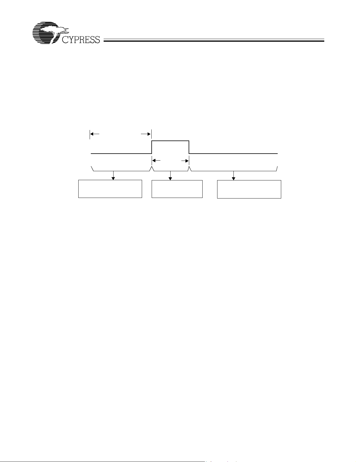
10.3 Watchdog Reset (WDR)
The Watchdog Timer Reset (WDR) occurs when the internal Watchdog timer rolls over. Writing any value to the write-only
Watchdog Reset Register at address 0x26 will clear the timer. The timer will roll over and WDR will occur if it is not cleared within
(see Figure 10-1) of the last clear. Bit 6 (Watchdog Reset bit) of the Processor Status and Control Register is set to record
t
WATCH
this event (see Section 20.0 for more details). A Watchdog Timer Reset typically lasts for 2–4 ms, after which the microcontroller
begins execution at ROM address 0x0000.
t
WATCH = 10.1 to
14.6 ms
WDR
(at F
OSC
= 6 MHz)
2–4 ms
At least 10.1 ms
since last write to WDR
WDR goes HIGH
for 2–4 ms
Execution begins at
ROM Address 0x0000
Figure 10-1. Watchdog Reset (WDR, Address 0x26)
11.0 Suspend Mode
The CY7C637xx parts support a versatile low-power suspend mode. In suspend mode, only an enabled interrupt or a LOW state
on the D–/SDATA pin will wake the part. Two options are available. For lowest power, all internal circuits can be disabled, so only
an external event will resume operation. Alternatively, a low-power internal wake-up timer can be used to trigger the wake-up
interrupt. This timer is described in Section 11.2, and can be used to periodically poll the system to check for changes, such as
looking for movement in a mouse, while maintaining a low average power.
The CY7C637xx is placed into a low-power state by setting the Suspend bit of the Processor Status and Control Register
(Figure 20-1). All logic blocks in the device are turned off except the GPIO interrupt logic, the D–/SDATA pin input receiver, and
(optionally) the wake-up timer. The clock oscillators, as well as the free-running and watchdog timers are shut down. Only the
occurrence of an enabled GPIO interrupt, wake-up interrupt, SPI slave interrupt, or a LOW state on the D–/SDATA pin will wake
the part from suspend (D– LOW indicates non-idle USB activity). Once one of these resuming conditions occurs, clocks will be
restarted and the device returns to full operation after the oscillator is stable and the selected delay period expires. This delay
period is determined by selection of internal vs. external clock, and by the state of the Ext. Clock Resume Delay as explained in
Section 9.0.
In suspend mode, any enabled and pending interrupt will wake the part up. The state of the Interrupt Enable Sense bit (Bit 2,
Figure 20-1) does not have any effect. As a result, any interrupts not intended for waking from suspend should be disabled through
the Global Interrupt Enable Register and the USB End Point Interrupt Enable Register (Section 21.0).
If a resuming condition exists when the suspend bit is set, the part will still go into suspend and then awake after the appropriate
delay time. The Run bit in the Processor Status and Control Register must be set for the part to resume out of suspend.
Once the clock is stable and the delay time has expired, the microcontroller will execute the instruction following the I/O write that
placed the device into suspend mode before servicing any interrupt requests.
To achieve the lowest possible current during suspend mode, all I/O should be held at either V
bit interrupts (Figure 21-4 and Figure 21-5) should be disabled for any pins that are not being used for a wake-up interrupt. This
or ground. In addition, the GPIO
CC
should be done even if the main GPIO Interrupt Enable (Figure 21-1) is off.
Typical code for entering suspend is shown below:
... ; All GPIO set to low-power state (no floating pins, and bit interrupts disabled unless using for wake-up)
... ; Enable GPIO and/or wake-up timer interrupts if desired for wake-up
... ; Select clock mode for wake-up (see Section 11.1)
mov a, 09h ; Set suspend and run bits
iowr FFh ; Write to Status and Control Register - Enter suspend, wait for GPIO / wake-up interrupt or USB activity
nop ; This executes before any ISR
... ; Remaining code for exiting suspend routine
Document #: 38-08022 Rev. ** Page 17 of 58
FOR
FOR
enCoRe™ USB CY7C63722/23
CY7C63743
11.1 Clocking Mode on Wake-up from Suspend
When exiting suspend on a wake-up event, the device can be configured to run in either Internal or External Clock mode. The
mode is selected by the state of the External Oscillator Enable bit in the Clock Configuration Register (Figure 9-2). Using the
Internal Clock saves the external oscillator start-up time and keeps that oscillator off for additional power savings. The external
oscillator mode can be activated when desired, similar to operation at power-up.
The sequence of events for these modes is as follows:
Wake in Internal Clock Mode:
1. Before entering suspend, clear bit 0 of the Clock Configuration Register. This selects Internal clock mode after suspend.
2. Enter suspend mode by setting the suspend bit of the Processor Status and Control Register.
3. After a wake-up event, the internal clock starts immediately (within 2 µs).
4. A time-out period of 8 µs passes, and then firmware execution begins.
5. At some later point, to activate External Clock mode, set bit 0 of the Clock Configuration Register. This halts the internal clocks
while the external clock becomes stable. After an additional time-out (128 µs or 4 ms, see Section 9.0), firmware execution
resumes.
Wake in External Clock Mode:
1. Before entering suspend, the external clock must be selected by setting bit 0 of the Clock Configuration Register. Make sure
this bit is still set when suspend mode is entered. This selects External clock mode after suspend.
2. Enter suspend mode by setting the suspend bit of the Processor Status and Control Register.
3. After a wake-up event, the external oscillator is started. The clock is monitored for stability (this takes approximately 50–100 µs
with a ceramic resonator).
4. After an additional time-out period (128 µs or 4 ms, see Section 9.0), firmware execution resumes.
11.2 Wake-up Timer
The wake-up timer runs whenever the wake-up interrupt is enabled, and is turned off whenever that interrupt is disabled.
Operation is independent of whether the device is in suspend mode or if the global interrupt bit is enabled. Only the Wake-up
Timer Interrupt Enable bit (Figure 21-1) controls the wake-up timer.
Once this timer is activated, it will give interrupts after its time-out period (see below). These interrupts continue periodically until
the interrupt is disabled. Whenever the interrupt is disabled, the wake-up timer is reset, so that a subsequent enable always
results in a full wake-up time.
The wake-up timer can be adjusted by the user through the Wake-up Timer Adjust bits in the Clock Configuration Register
(Figure 9-2). These bits clear on reset. In addition to allowing the user to select a range for the wake-up time, a firmware algorithm
can be used to tune out initial process and operating condition variations in this wake-up time. This can be done by timing the
wake-up interrupt time with the accurate 1.024-ms timer interrupt, and adjusting the Timer Adjust bits accordingly to approximate
the desired wake-up time.
Table 11-1. Wake-up Timer Adjust Settings
Adjust Bits [2:0]
(Bits [6:4] in Figure 9-2) Wake-up Time
000 (reset state) 1 * t
001 2 * t
010 4 * t
011 8 * t
100 16 * t
101 32 * t
110 64 * t
111 128 * t
See Section 26.0 for the value of t
WAKE
WAKE
WAKE
WAKE
WAKE
WAKE
WAKE
WAKE
WAKE
12.0 General Purpose I/O Ports
Ports 0 and 1 provide up to 16 versatile GPIO pins that can be read or written (the number of pins depends on package type).
Figure 12-1 shows a diagram of a GPIO port pin.
Document #: 38-08022 Rev. ** Page 18 of 58
 Loading...