

CYPRESS CY7C63742 User Manual

enCoRe
PRELIMINARY
USB™ CY7C63722/23
CY7C63742/43
CY7C63722/23
CY7C63742/43
enCoRe™
USB
Combination Low-Speed USB & PS/2
Peripheral Controller
Cypress Semiconductor Corporation
• 3901 North First Street • San Jose • CA 95134 • 408-943-2600
May 25, 2000

FOR
FOR
enCoRe™
USB CY7C63722/23
PRELIMINARY
CY7C63742/43
TABLE OF CONTENTS
1.0 FEATURES .....................................................................................................................................5
2.0 FUNCTIONAL OVERVIEW .............................................................................................................6
2.1 enCoRe USB - The New USB Standard .......................................................................................6
3.0 LOGIC BLOCK DIAGRAM .............................................................................................................7
4.0 PIN CONFIGURATIONS .................................................................................................................7
5.0 PIN ASSIGNMENTS .......................................................................................................................7
6.0 PROGRAMMING MODEL ...............................................................................................................8
6.1 Program Counter (PC) ...................................................................................................................8
6.2 8-bit Accumulator (A) ....................................................................................................................8
6.3 8-bit Index Register (X) ..................................................................................................................8
6.4 8-bit Program Stack Pointer (PSP) ...............................................................................................8
6.5 8-bit Data Stack Pointer (DSP) ......................................................................................................8
6.6 Address Modes ..............................................................................................................................9
6.6.1 Data ........................................................................................................................................................9
6.6.2 Direct .....................................................................................................................................................9
6.6.3 Indexed ..................................................................................................................................................9
7.0 INSTRUCTION SET SUMMARY ...................................................................................................10
8.0 MEMORY ORGANIZATION ..........................................................................................................11
8.1 Program Memory Organization .................................................................................................. 1 1
8.2 Data Memory Organization .........................................................................................................12
8.3 I/O Register Summary .................................................................................................................13
9.0 CLOCKING ....................................................................................................................................14
9.1 Internal / External Oscillator Operation .....................................................................................15
9.2 External Oscillator .......................................................................................................................15
10.0 RESET .........................................................................................................................................15
10.1 Low Voltage Reset (LVR) ..........................................................................................................16
10.2 Brown Out Reset (BOR) ......... ............... ... ............... ............... .............. ............... ...................... 1 6
10.3 Watch Dog Reset (WDR) ....................... .............. ............... .... .............. ............... ...................... 1 6
11.0 SUSPEND MODE ..................... ............... .............. ............... ............... .............. ..........................1 6
11.1 Clocking Mode on Wake-up from Suspend .............................................................................1 7
11.2 Wake-up Timer ...........................................................................................................................17
12.0 GENERAL PURPOSE I/O PORTS .............................................................................................18
12.1 Auxiliary Input Port ................................ .............. ............... ............... .............. ..........................2 0
13.0 USB SERIAL INTERFACE ENGINE (SIE) .................................................................................20
13.1 USB Enumeration ......................................................................................................................21
13.2 USB Port Status and Control ....................................................................................................21
14.0 USB DEVICE ...............................................................................................................................22
14.1 USB Address Register ..............................................................................................................2 2
14.2 USB Control Endpoint ...............................................................................................................22
14.3 USB Non-Control Endpoints (2) ............................................................................................... 2 3
14.4 USB Endpoint Counter Registers ............................................................................................ 2 3
15.0 USB REGULATOR OUTPUT ......................................................................................................24
2

FOR
FOR
enCoRe™
USB CY7C63722/23
PRELIMINARY
TABLE OF CONTENTS
(continued)
CY7C63742/43
16.0 PS/2 OPERATION ...... .............. ............... .............. ............... ............... .............. ..........................24
17.0 SERIAL PERIPHERAL INTERFACE (SPI) .................................................................................25
17.1 Operation as an SPI Master ......................................................................................................26
17.2 Master SCK Selection ................................................................................................................26
17.3 Operation as an SPI Slave ........................................................................................................2 7
17.4 SPI Status and Control ..............................................................................................................27
17.5 SPI Interrupt ...............................................................................................................................28
17.6 SPI modes for GPIO pins ..........................................................................................................28
18.0 12-BIT FREE-RUNNING TIMER .................................................................................................29
19.0 TIMER CAPTURE REGI STERS ........................... ............... ............... .............. ............... ...........30
20.0 PROCESSOR STATUS AND CONTROL REGISTER ............ .............. ............... ............... .......32
21.0 INTERRUPTS ..............................................................................................................................33
21.1 Interrupt Vectors ........................................................................................................................34
21.2 Interrupt Latency .......................................................................................................................35
21.3 Interrupt Sources .......................................................................................................................35
21.3.1 USB Bus Reset or PS/2 Activit y ............... ......... .......................... .......... .......................... ................35
21.3.2 Free Running Timer Interrupts ........................................................................................................35
21.3.3 USB Endpoint Int e r ru pts ................... .......... ......... .......... ......... .........................................................35
21.3.4 SPI Inte rru pt .. ......... .......... .................................................................................... .............................35
21.3.5 Capture Timer Interrupts .................................................................................................................35
21.3.6 GPIO Inte rrupt ... .......... ......... .......... ................................. ......... .......... ......... ......................................35
21.3.7 Wake-up Interrupt .............................................................................................................................37
22.0 USB MODE TABLES ..................................................................................................................37
23.0 ABSOLUTE MAXIMUM RATINGS .............................................................................................4 0
24.0 DC CHARACTERISTICS ............................................................................................................4 1
25.0 SWITCHING CHARACTERISTICS .............................................................................................4 2
26.0 ORDERING INFORMATION .......................................................................................................47
27.0 PACKAGE DIAGRAMS ..............................................................................................................47
LIST OF FIGURES
Figure 8-1. Program Memory Space with Interrupt Vector Table ..................................................11
Figure 9-1. Clock Oscillator On-chip Circuit ...................................................................................14
Figure 9-2. Clock Configuration Register (Address 0xF8) .............................................................14
Figure 10-1. Watch Dog Reset (WDR) ..............................................................................................16
Figure 12-1. Block Diagram of GPIO P ort (one pin shown) ............... ............... .............. ...............18
Figure 12-2. Port 0 Data (Add r ess 0x00)
..........................................................................................19
Figure 12-3. Port 1 Data (Address 0x01) ..........................................................................................19
Figure 12-4. GPIO Port 0 Mode0 Register (Address 0x0A) ............................................................19
Figure 12-5. GPIO Port 0 Mode1 Register (Address 0x0B) ............................................................20
Figure 12-6. GPIO Port 1 Mode0 Register (Address 0x0C) ............................................................20
Figure 12-7. GPIO Port 1 Mode1 Register (Address 0x0D) ............................................................20
Figure 12-8. Port 2 Data Register (Address 0x02) .............................. ............... .............. ...............20
Figure 13-1. USB Status and Control Register (Address 0x1F) ....................................................21
Figure 14-1. USB Device Address Register (Address 0x10) ..........................................................22
Figure 14-2. USB EP0 Mode Register (Address 0x12) ....................................................................22
3

FOR
FOR
enCoRe™
USB CY7C63722/23
PRELIMINARY
LIST OF FIGURES
(continued)
CY7C63742/43
Figure 14-3. USB Endpoint EP1, EP2 Mode Registers (Addresses 0x14, 0x16) ..........................2 3
Figure 14-4. USB Device Counter Registers (Addresses 0x11h, 0x13h, 0x15) ............................23
Figure 16-1. Diagram of USB - PS/2 Syste m Connections ............. ............... ............... .............. ....25
Figure 17-1. SPI Block Diagram ........................................................................................................26
Figure 17-2. SPI Data Register (Address 0x60) ...............................................................................26
Figure 17-3. SPI Control Register (Address 0x61) ..........................................................................27
Figure 17-4. SPI Data Timing ............................................................................................................28
Figure 18-1. Timer LSB Register (Address 0x24) ...........................................................................29
Figure 18-2. Timer MSB Register (Address 0x25) ...........................................................................29
Figure 18-3. Timer Block Diagram ....................................................................................................29
Figure 19-1. Capture Timers Block Diagram ...................................................................................30
Figure 19-2. Capture Timer A-Rising, Data Register (Address 0x40) ...........................................31
Figure 19-3. Capture Timer A-Falling, Data Register (Address 0x41) ......................... .............. ....31
Figure 19-4. Capture Timer B-Rising, Data Register (Address 0x42) ...........................................31
Figure 19-5. Capture Timer B-Falling, Data Register (Address 0x43) ......................... .............. ....31
Figure 19-6. Capture Timers Configuration Register (Address 0x44) ............. .............. ...............31
Figure 19-7. Capture Timers Status Register (Address 0x45) .......................................................31
Figure 20-1. Processor Status and Control Register (Address 0xFF) ..........................................32
Figure 21-1. Global Interrupt Enable Register 0x20h (read/write) .................... .............. ...............33
Figure 21-2. USB End Point Interrupt Enable Register (Address 0x21) .......................................33
Figure 21-3. Interrupt Controller Logic Block Diagram ..................................................................34
Figure 21-4. Port 0 Interrupt Enable Register (Address 0x04) ....... ............... ............... .............. ....36
Figure 21-5. Port 1 Interrupt Enable Register (Address 0x05) ....... ............... ............... .............. ....36
Figure 21-6. Port 0 Interrupt Polarity Register (Address 0x06) .....................................................36
Figure 21-7. Port 1 Interrupt Polarity Register (Address 0x07) .....................................................36
Figure 21-8. GPIO Interrupt Diagram ............................. ............... .............. ............... ............... .. .....36
Figure 25-1. Clock Timing ..................... ............... ............... .............. ............... ............... ..................43
Figure 25-2. USB Data Signal Timing ...................... .............. ............... ............... .............. ............... 4 3
Figure 25-3. Receiver Jitter Tolerance ......... .............. ............... ............... .............. ............... ...........44
Figure 25-4. Differential to EOP Transition Skew and EOP Widt h ...................... ............... ...........44
Figure 25-5. Differential Data Jitter ..................................................................................................44
Figure 25-7. SPI Slave Timing, CPHA=0 ..........................................................................................45
Figure 25-6. SPI Master Timing, CPHA=0 ........................................................................................45
Figure 25-8. SPI Master Timing, CPHA=1 ........................................................................................46
Figure 25-9. SPI Slave Timing, CPHA=1 ..........................................................................................46
LIST OF TABLES
Table 8-1. I/O Register Summary ......................................................................................................1 3
Table 11-1. Wake-up Timer Adjust Settings .................................................................................... 18
Table 12-1. Ports 0 and 1 Output Control Truth Table ...................................................................19
Table 13-1. Control Modes to Force D+/D– Outputs .......................................................................22
Table 17-1. SPI Control Register Definitions ...................................................................................27
Table 17-2. SPI Pin Assignments .....................................................................................................28
Table 19-1. Capture Timer Prescalar Settings (Step size and range for FCLK = 6 MHz) ............ 3 2
Table 21-1. Interrupt Vector Assignments .......................................................................................34
Table 22-1. USB Register Mode Encoding ......................................................................................37
Table 22-2. Decode table for
Table 22-3
: “Details of Modes for Differing Traffic Conditions” ...3 8
Table 22-3. Details of Modes for Differing Traffic Conditions .......................................................39
4

FOR
FOR
enCoRe™
USB CY7C63722/23
PRELIMINARY
CY7C63742/43
1.0 Features
• enCoRe™ USB - enhanced Component Reduction
—Internal oscillator eli m inates the need for an exte rnal crystal or resonator
—Interface can auto-configure to opera te as PS/2 or USB without the need for external components to switch between
modes (no GPIO pins needed to manage dual mode capability)
—Internal 3.3V regulator for USB pull-up resistor
—Configurable GPIO for real-world interface without external components
• Flexible, cost-effective solution for applications that combine PS/2 and low-speed USB, such as mice, gamepads,
joysticks, and many others.
• USB Specification Complia nce
—Conforms to USB Specification, Version 1.1
—Conforms to USB HID Specification, Version 1.1
—Supports 1 Low-Speed USB device address and 3 data endpoints
—Integrated USB transceiver
—3.3V regulated output for USB pull-up resist or
• 8-bit RISC microcontroller
—Harvard architecture
—6-MHz external ceramic resonator or internal clock mode
—12-MHz internal CPU clock
—Internal memory
—256 bytes of RAM
—6 Kbytes of EPROM (CY7C63722, CY7C63742)
—8 Kbytes of EPROM (CY7C63723, CY7C63743)
—Interface can auto-configure to operate as PS/2 or USB
—No external components for switching between PS/2 and USB modes
—No GPIO pins needed to manage dual mode capability
• I/O ports
—Up to 16 versatile General Purpose I/O (GPIO) pins, individually configurable
—High current drive on any GPIO pin: 50 mA/pin current sink
—Each GPIO pin supports high-impedance i nputs, internal pull-ups, open dr ain outputs or traditional CMOS outputs
—Maskable interrupts on all I/O pins
• SPI serial communication block
—Master or slave operation
—2 Mbit/s transfers
• Four 8-bit Input Capture registers
—Two registers each for two input pins
—Capture timer setting with 5 pre-scaler settings
—Separate registers for rising and falling edge capture
—Simplifies interface to RF inputs f or wir eless applications
• Internal lo w -power wake-up timer during suspend mode
—Periodic wake-up with no external components
• Optional 6-MHz internal oscillator mode
—Allows fast start-up from suspend mode
• Watch dog timer (WDT)
• Low Voltage Reset at 3.75V
• Internal br own-out reset for suspend mode
• Improved output drivers to reduce EMI
• Operating vol tage from 4.0V to 5.5VDC
5

FOR
FOR
enCoRe™
USB CY7C63722/23
PRELIMINARY
• Operating temperature from 0 to 70 degrees Celsius
• CY7C63722/23 available in 18-pin PDIP
• CY7C63742/43 available in 24-pin SOIC, 24-pin PDIP
• Industry standard programmer support
CY7C63742/43
2.0 Functional Overview
2.1
Cypress has re-invented its leadership position in the low-speed USB market with a new family of innovative microcontrollers.
Introducing...
create a new family of low-speed USB microcontrollers that will enable peripheral developers to design new products with a
minimum number of components. At the heart of our
oscillator. By int egrat ing t he osc illato r into our chi p , an e xternal crystal o r resona tor is no longer need ed. We ha ve also integrated
other external components commonly found in low-speed USB applications such as pull-up resistors, wake-up circuitry, and a
3.3V regulator. All of this adds up to a lower system cost.
The CY7C63722/23 and CY7C63742/ 43 are 8-bit RISC One Time Progr ammable (O TP) mic rocontroll ers. The instructi on set has
been optimiz ed specif ical ly f or USB an d PS/ 2 opera tions , al though t he mi crocont roll ers ca n be u sed f or a va riety o f o ther embed ded applications.
The CY7C637xx features up to 16 general purpose I/O (GPIO) pins to support USB, PS/2 and other applications. The I/O pins
are grouped into two ports (Port 0 to 1) where each pin can be i ndividually configured as i nputs with internal pull-ups, open drain
outputs, or tr adit ional CMOS outpu ts with pr og rammab le driv e streng th o f up to 50 mA out put driv e . Addit ional ly, each I/O pin can
be used to gener at e a GPIO inte rrupt to t he mi crocont roll er . Note t he GPI O inter rupts all shar e the s ame “GPIO” int errupt vect or .
The CY7C637xx microcontrollers feature an internal 5% accurate 6-MHz clock source. Optionally, an external 6-MHz ceramic
resonator can be used to provide a highe r precision reference for USB operation. This cloc k generator reduces the clock-related
noise emissions (EMI). The clock generator provides the 6- and 12-MHz clocks that remain internal to the microcontrol ler.
The CY7C637xx is offered with two EPROM options to maximize flexibility and minimize cost. The CY7C637x2 has 6 Kbytes of
EPROM. The CY7 C637x3 has 8 Kbyt es of EPR OM. Al l v ersi ons hav e 2 56 b ytes of dat a RAM f or stac k spac e, u ser v ariab l es, and
USB FIFOs.
These parts include low-voltage reset logic, a watch dog timer, a vectored interrupt controller, a 12-bit free-running timer, and
capture timers. The l ow-voltage reset (LVR) logic detects when power is applied to the device, resets the logic to a known state,
and begins executing instructions at EPROM addres s 0x0000. LVR will also reset the part when V
voltage r ange. The watch dog timer can be used to ensure the firmware never gets stalled for more than approxim ately 8 ms.
The microcontroller supports 10 maskable interrupts in the vectored interrupt controller. Interrupt sources include the USB
Bus-Reset, the 128-µs and 1.024-ms outputs from the free-running timer, three USB endpoints, two capture timers, an internal
wake-up timer and the GPIO ports. The timers bits cause periodic interrupts when enabled. The USB endpoints interrupt after
USB transact ions c omple te on t he b us. Th e captur e ti mers in terrupt whene v er a ne w tim er v alue i s sav ed due to a sel ected GPIO
edge event. The GPIO ports have a level of masking to select which GPIO inputs can cause a GPIO interrupt. For additional
flexibility, the input transition polarity that causes an interrupt is programmable for each GPIO pin. The interrupt polarity can be
either rising or falling edge.
The free-running 12-bit timer clocked at 1 MHz provides two interrupt sources as noted above (128 µs and 1.024 ms ). The timer
can be used to measure the duration of an event under firmware control by reading the timer at the start and end of an event,
and subtracting the two values. The four capture timers save a programmable 8 bit range of t he free-running timer when a GPIO
edge occurs on the two capture pins (P0.0, P0.1).
The CY7C637xx incl udes an int egrat ed USB seri al int erf ace eng in e (SIE) that su pports the int egrat ed p eripher als. The har dwar e
supports one USB device ad dress with t hree endpoin ts. The SIE all ows the USB host to communicat e with the funct ion integr ated
into the microcontroller. A 3.3V regulated output pin provides a pull-up source for t he external USB resistor on the D– pin.
The USB D+ and D– USB pins can alternately be used as PS/2 SCLK and SDATA signals, so that products can be designed to
respond to either USB or PS/2 modes of operation. PS/2 operation is supported with internal pull-up resistors on SCLK and
SDATA, the ability to disable the re gulato r output pin, and an interru pt to signal t he start of PS/2 activity. No external components
are necessary fo r dual USB and PS/2 sys tems, and no GPIO pins need to be dedic ated to s witc hing betw een modes . Slo w edge
rates operate in both modes to reduce EMI.
enCoRe
USB - The New USB Standard
enCoRe
USB—“enhanced Componen t Reducti on.” Cy press has leveraged its design e xpertise in USB solutions to
enCoRe
TM
USB technology is the breakthrough design of a crystal-less
drops below the operat ing
CC
6
FOR
FOR
enCoRe™
USB CY7C63722/23
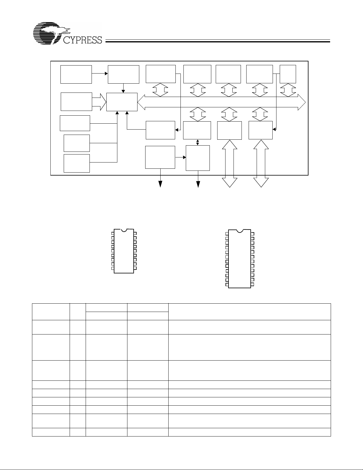
3.0 Logic Block Diagram
Internal
Oscillator
Oscillator
EPROM
6K/8 K B yte
Brown-out
Reset
Watch
Dog
Timer
Low
Voltage
Reset
4.0 Pin Configurations
CY7C63722/23
18-pin PDIP
P0.0
P0.1
P0.2
P0.3
VSS
VPP
VREG
XTALIN/P2.1
PRELIMINARY
Xtal
8-bit
RISC
core
1
2
3
4
5
6
7
8
9
18
17
16
15
14P1.0
13
12
11
10
Wake-Up
Interrupt
Contro ller
Regulator
P0.4
P0.5
P0.6
P0.7
P1.1
D+/SCLK
D–/SDATA
VCC
XTALOUT
Timer
3.3V
VREG
256 Byte
Top View
RAM
USB
Engine
USB &
PS/2
Xcvr
D+,D–
12-bit
Timer
Port 1
GPIO
P1.0–P1.7
CY7C63742/43
24-pin SOIC/PDIP
P0.0
P0.1
P0.2
P0.3
P1.0
P1.2
P1.4
P1.6
VSS
VPP
VREG
XTALIN/P2.1
CY7C63742/43
Capture
Timers
Port 0
GPIO
P0.0–P0.7
24
23
22
21
20
19
18
17
16
15
14
13
P0.4
P0.5
P0.6
P0.7
P1.1
P1.3
P1.5
P1.7
D+/SCLK
D–/SDATA
VCC
XTALOUT
1
2
3
4
5
6
7
8
9
10
11
12
SPI
5.0 Pin Assignments
CY7C63722/23 CY7C63742/43
Name I/O
D–/SDATA,
D+/SCLK
P0[7:0] I/O 1, 2, 3, 4,
I/O 12
13
15, 16, 17, 18
15
16
1, 2, 3, 4,
21, 22, 23, 24
P1[7:0] I/O 5, 14 5, 6, 7, 8,
17, 18, 19, 20
XTALIN/P2.1 IN 9 12 6-MHz cerami c resonator or ext ernal clock input, or P2.1 input
XTALOUT OUT 10 13 6-MHz cerami c resonator return pin or internal oscillator output
V
PP
V
CC
7 10 Programming v oltage supply, ground for normal oper ati on
11 14 V olt age supply
VREG/P2.0 8 11 Vo ltage su ppl y for 1.5-kΩ USB pull-up resistor (3.3V nomi nal). Als o
V
SS
6 9 Ground
Description18-Pin 24-Pin
USB diff erential data lines (D– and D+), or PS/2 clock and data signals (SDATA and SCLK)
GPIO Po rt 0 capable of sinking up t o 50 mA/pin, or sinking co ntrolled
low or high prog rammable current. Can also source 2 mA current,
provide a res istive pul l-up , or serve as a high impedance input. P0. 0
and P0.1 provi de inputs to Capture Timers A and B, respect ively.
IO Port 0 capable of sinking up to 50 mA/pin, or sinking controlled
low or high prog rammable current. Can also source 2 mA current,
provide a resistive pull-up, or serve as a high impedance input.
serves as P2.0 input.
7

FOR
FOR
enCoRe™
USB CY7C63722/23
PRELIMINARY
CY7C63742/43
6.0 Programming Model
Refer to the
6.1 Program Counter (PC)
The 13-bit program counter (PC) allows access for up to 8 Kbytes of EPROM using the CY7C637xx architecture. The program
counter is cleared during res et, such that the first instruction executed after a reset is at ad dress 0x0000. This is typically a jump
instruction to a res et handler that initializes the applicat ion.
The lower 8 bi ts of the progr am counter are incremented as i nstructio ns are loaded and e xecu ted. The upp er 5 bits of the pr ogram
counter are increment ed by executing an XPAGE instruction. As a result, the last instruction executed within a 256-byte “page”
of sequential code should be an XPAGE instruction. The assembler directive “XPAGEON” will ca use the assembler to inser t
XPAGE instructions automatically. As instructions can be either one or two bytes long, the assembler may occasionally need to
insert a NOP followed by an XPAGE for correct execution.
The program counte r of t he ne xt i nstruct ion t o be e x ecut ed, car ry flag, and z er o fla g are sav ed a s two b yt es on the prog ram stack
during an interrupt acknowledge or a CALL instruction. The program counter, carry flag, and zer o flag are restored from the
program stack only during a RETI instructio n.
Please note the program counter cannot be accessed directly by the firmware. The progr am stack can be examined by reading
SRAM from locat ion 0x00 and up.
6.2 8-bit Accumulator (A)
The accumulator is the general purpose, do everything register in the architecture where results are usually calculated.
6.3 8-bit Index Register (X)
The inde x r egist er “X” is availabl e to the firmware as an auxiliary accu mulator . The X register also allows the processor to perf orm
indexed operations by loading an index value into X.
CYASM Assembler User’s Guide
for more details on f irmwar e operation with the CY7C637xx mic rocontrollers.
6.4 8-bit Program Stack Pointer (PSP)
During a reset, the pr ogram stack pointer (PSP) is set to zero. This m eans the program “stack” starts at RAM address 0x00 and
“grows” upward from there . Note the prog ram stac k pointe r is directl y address ab le under firmware control , using the MO V PSP,A
instruction. The PSP supports interrupt service under hardware control and CALL, RET, and RETI instructions under firmware
control.
During an interrupt acknowledge, interrupts are disabled and the program counter, carry flag, and zero flag are written as two
bytes of data memory . The first byte is stor ed in the memory addressed by the progr am stack pointe r, then the PSP is inc remented.
The second b yte is stored in memory addressed by the program stac k pointer and the PSP is incremented again. Th e net effect
is to store the progr am cou nter and flags on the program “stack” and increment the program stack pointer by two.
The return from interrupt (RETI) instruction decrements the program stack pointer, then restores the second byte from memory
addressed by the PSP. The program stack pointer is decremented again and the first byte is restored from memory addressed
by the PSP. Aft er th e prog r am cou nter and flags hav e be en rest ored fr om stac k, the inte rrupts are en ab le d. The eff e ct i s to res tore
the program counter and flags from the program stack, decrement the pr ogram stack pointer by two, and re-enable interrupt s.
The call subr outine (CAL L) instruction s tores the p rogram counter and flags on t he progra m stack and incremen ts the PSP b y two .
The return fr om subr out ine ( RET) ins tructi on re sto res t he prog r am co unter, but not th e fla gs, from pr og ram stac k and decrement s
the PSP by two.
Note that t here ar e rest ricti ons i n us ing some ju mp , cal l, a nd index instructions across the 4KB boundary of the prog ram memory.
Refer to the
CYASM Assembler User’s Guide
for a detailed description.
6.5 8-bit Data Stack Pointer (DSP)
The data stack pointer (DSP) supports PUSH and POP instructions that use the data stack for temporary storage. A PUSH
instruction wi ll pre- decr ement th e DSP, then write data to t he memory l ocatio n address ed b y the DSP. A POP instruction will rea d
data from the memory location addressed by the DSP, then post-increment the DSP.
During a reset, the Data Stack Poi nter will be set to zero. A PUSH instruction when DSP equal zero will write data at th e to p of
the data RAM (address 0xFF). This would write data to the memory area reserved for a FIFO for USB endpoint 0. In non-USB
applications, this works fine and is not a prob lem.
8

FOR
FOR
enCoRe™
USB CY7C63722/23
PRELIMINARY
For USB appl icati ons, the fi rmware sh ould set the DSP t o an a ppropria te loc ation to av o id a memory conf lict wi th RAM dedicat ed
to USB FIFOs. The memory requirements for the USB endpoints are shown in Section 8.2. For example, assembly instructions
to set the DSP to 20h (giving 32 bytes for program and data stack combined) are shown below:
MOV A,20h ; Move 20 hex into Accumulator (must be D8h or le ss to avoid USB FIFOs)
SWAP A,DSP ; swap accumulator value into DSP register
CY7C63742/43
6.6 Address Modes
The CY7C637xx microcontrollers support three addressing modes for instructions that require data operands: data, direct, and
indexed.
6.6.1 Data
The “Data” address mode ref er s to a da ta operand that i s a ctual ly a con stant encod ed in t he inst ructi on. As an e xa mple, cons ider
the instruction that loads A with the constant 0x30:
• MOV A, 30h
This instruction will require two bytes of code where the first byte identifies the “MOV A” instruction with a data operand as the
second byte. The second byt e of the instruction will be the constant “0xE8h”. A constant may be referred to by name if a prior
“EQU” statement assigns the constant value to the name. For example, the following code is equivalent to the example shown
above:
• DSPINIT: EQU 30h
• MOV A,DSPINIT
6.6.2 Direct
“Direct” address mode is used when the data operand is a variable stored in SRAM. In that case, the one byte address of the
variable is encoded in the instruction. As an example, consider an instruction that loads A with the contents of memory address
location 0x10h:
• MOV A, [ 10h]
In normal usage, variable nam es are assigned to var iable addresses using “EQU” statements to improve the readability of the
assembl er source code. As an example, the following code is equivalent to the example shown above:
• buttons: EQU 10h
• MOV A,[buttons]
6.6.3 Indexed
“Indexed” address mode allows the firmware to manipulate arrays of data stored in SRAM. The address of the data operand is
the sum of a constant encoded in the instruction and the contents of the “X” register. In normal usage, the constant will be the
“base” address of an array of data and the X register will contain an index that indicates which element of the array is actually
addressed:
• array: EQU 10h
• MOV X,3
• MOV A,[x+array]
This would have the effect of loading A with the fourth element of the SRAM “array” that begins at address 0x10h. The fourth
element would be at add ress 0x13h.
9
FOR
FOR
enCoRe™
USB CY7C63722/23
PRELIMINARY
CY7C63742/43
7.0 Instructio n Set Summary
Refer to the
HALT 00 7 NOP 20 4
ADD A,expr data 01 4 INC A acc 21 4
ADD A,[expr] direct 02 6 INC X x 22 4
ADD A,[X+expr] index 03 7 INC [expr] direct 23 7
ADC A,expr data 04 4 INC [X+expr] index 24 8
ADC A,[expr] direct 05 6 DEC A acc 25 4
ADC A,[X+expr] index 06 7 DEC X x 26 4
SUB A,expr data 07 4 DEC [expr] direct 27 7
SUB A,[expr] direct 08 6 DEC [X+expr] index 28 8
SUB A,[X+expr] index 09 7 IORD expr address 29 5
SBB A,expr data 0A 4 IOWR expr address 2A 5
SBB A,[expr] direct 0B 6 POP A 2B 4
SBB A,[X+expr] index 0C 7 POP X 2C 4
OR A, ex pr data 0D 4 PUSH A 2D 5
OR A,[expr] direct 0E 6 PUSH X 2E 5
OR A,[X+expr] index 0F 7 SWAP A,X 2F 4
AND A,expr data 10 4 SWAP A,DSP 30 4
AND A,[expr] direct 11 6 MO V [expr],A direct 31 5
AND A,[X+expr] index 12 7 MOV [X+expr],A index 32 6
XOR A,expr data 13 4 OR [expr],A direct 33 7
XOR A,[expr] direct 14 6 OR [X+expr],A index 34 8
XOR A,[X+expr] index 15 7 AND [expr],A direct 35 7
CMP A,expr data 16 5 AND [X+expr],A index 36 8
CMP A,[expr] direct 17 7 XOR [expr],A direct 37 7
CMP A,[X+expr] index 18 8 XOR [X+expr],A index 38 8
MOV A,expr data 19 4 IOWX [X+expr] index 39 6
MOV A,[ex pr] direct 1A 5 CPL 3A 4
MOV A,[X+expr] index 1B 6 ASL 3B 4
MOV X,expr data 1C 4 ASR 3C 4
MOV X,[ex pr] direct 1D 5 RLC 3D 4
reserved
XPAGE 1F 4 RET 3F 8
MOV A,X 40 4 DI 70 4
MOV X,A 41 4 EI 72 4
MOV PSP,A 60 4 RETI 73 8
CALL addr 50 - 5F 10
JMP addr 80-8F 5 JC addr C0-CF 5
CALL addr 90-9F 10 JNC addr D0-DF 5
JZ addr A0-AF 5 JACC addr E0-EF 7
JNZ addr B0-BF 5 INDEX addr F0-FF 14
CYASM Assembler User’s Guide
MNEMONIC operand opcode cycles MNEMONIC operand opcode cycles
for det ailed information on these instructions.
1E RRC 3E 4
10
FOR
FOR
enCoRe™
USB CY7C63722/23
PRELIMINARY
8.0 Memory Organization
8.1 Program Memory Organization
After re s e t Address
13 -bit PC 0x0000 Program execution begins here after a reset.
CY7C63742/43
0x0002 USB Bus Reset interrupt vector
0x0004 128-µs timer interrupt vector
0x0006 1.024-ms timer interrupt vector
0x0008 USB endpoint 0 interrupt vector
0x000A USB endpoint 1 interrupt vecto r
0x000C USB endpoint 2 interrupt vecto r
0x000E SPI interrupt vector
0x0010 Capture timer A interrupt Vector
0x0012 Capture timer B interrupt vector
0x0014 GPIO inte r r u pt vec tor
0x0016 Wake-up i n terrupt vector
0x0018
0x0FFF
0x17FF
0x1FDF 8 KB PROM ends here (CY7C63723, CY7C63743)
Program Memory begins here
4 KB
6 KB PROM ends here (CY7C63722, CY7C63742)
(8K - 32 bytes)
Figure 8-1. Program Memory Space with Interrupt Vector Table
11
FOR
FOR
enCoRe™
USB CY7C63722/23
PRELIMINARY
CY7C63742/43
8.2 Data Memory Organization
The CY7C637xx microcontrollers provide 256 bytes of data RAM. In normal usage, the SRAM is partitioned into four areas:
program stack, data stack , user variables and USB endpoint FIFOs as shown below:
After re s e t Address
8-bit D S P 8-bit PSP 0x00
(Move DSP)
8-bit DSP user selected
User Var iables
0xE8
USB FIFO for Address A endpoint 2
0xF0
USB FIFO for Address A endpoint 1
Program Stack Gr owth
Data Stack Growth
0xF8
Top of RAM Memory 0xFF
USB FIFO for Address A endpoint 0
12
FOR
FOR
enCoRe™
USB CY7C63722/23
PRELIMINARY
CY7C63742/43
8.3 I/O Register Summary
I/O registers are accessed via the I/O Read (IORD) and I/O Write ( IOWR, IOWX) instructions. IORD reads the selected port into
the accumulator. IOWR writes data from the accumulator to the selected port. Indexed I/O Write (IOWX) adds the contents of X
to the address in the instruction to form the port address and writes data from the accumulator to the specified port. Note that
specifying address 0 with IOWX (e.g., IOW X 0h) means the I/O port is selected solely by the contents of X.
Note: All bits of all registers are cleared to all zeros on reset,
All registers not listed are reserved, and should never be written by firmware. All bits marked as reserved should always
0xFF).
be written as 0.
Table 8-1. I/O Register Summary
Register Name I/O Address Read/Write Function Fig.
Port 0 Data 0x00 R/W GPIO Port 0 12-2
Port 1 Data 0x01 R/W GPIO Port 1 12-3
Port 2 Data 0x02 R Auxiliary input regis ter for D+, D–, VREG, XTALIN 12-8
Port 0 Interrupt Enabl e 0x04 W Interrupt enable for pins in Port 0 21-4
Port 1 Interrupt Enabl e 0x05 W Interrupt enable for pins in Port 1 21-5
Port 0 Interrupt Polarity 0x06 W Interrupt polarity for pins in Port 0 21-6
Port 1 Interrupt Polarity 0x07 W Interrupt polarity for pins in Port 1 21-7
Port 0 Mode0 0x0A W Controls output configuration for Port 0 12-4
Port 0 Mode1 0x0B W 12-5
Port 1 Mode0 0x0C W Controls output configuration for Port 1 12-6
Port 1 Mode1 0x0D W 12 -7
USB Device Address 0x10 R/W USB Device Address register 14-1
EP0 Counter Register 0x11 R/W USB Endpoint 0 counter regi ster 14-4
EP0 Mode Register 0x12 R/W USB Endpoint 0 configuration register 14-2
EP1 Counter Register 0x13 R/W USB Endpoint 1 counter regi ster 14-4
EP1 Mode Register 0x14 R/W USB Endpoint 1 configuration register 14-3
EP2 Counter Register 0x15 R/W USB Endpoint 2 counter regi ster 14-4
EP2 Mode Register 0x16 R/W USB Endpoint 2 configuration register 14-3
USB Status & Control 0x1F R/W USB status and control re gister 13-1
Global Interrupt Enable 0x20 R/W Global interrupt enable register 21-1
Endpoint Interrupt Enab le 0x21 R/W USB endpoint interrupt enables 21-2
Timer (LSB) 0x24 R Lower 8 bits of free-running timer (1 MHz) 18-1
Timer (MSB) 0x25 R Upper 4 bits of free-running timer 18-2
WDR Clear 0x26 W Watch Dog Reset clear -
Capture Timer A Rising 0x40 R Rising edge Capture Timer A data register 19-2
Capture Timer A Fa ll ing 0x41 R Falling edge Capture Timer A data register 19-3
Capture Timer B Rising 0x42 R Rising edge Capture Timer B data register 19-4
Capture Timer B Fa ll ing 0x43 R Falling edge Capture Timer B data register 19-5
Capture TImer Conf iguration 0x44 R/W Capture Timer configuration register 19-6
Capture Timer Status 0x45 R Capture Timer status register 19-7
SPI Data 0x60 R/W SPI read and write data register 17-2
SPI Control 0x61 R/W SPI status and control register 17-3
Clock Configuration 0xF8 R/W Internal / External Clock configuration register 9-2
Processor Status & Control 0xFF R/W Processor status and contr ol 20-1
except the Processor Status and Control Register (address
13
FOR
FOR
enCoRe™
USB CY7C63722/23
PRELIMINARY
CY7C63742/43
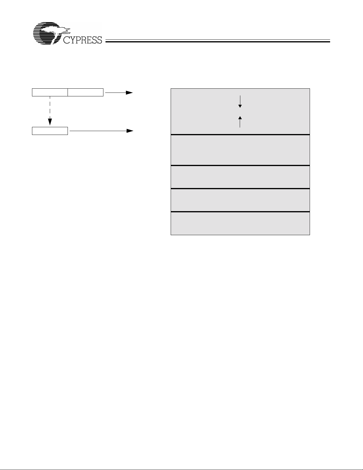
9.0 Clocking
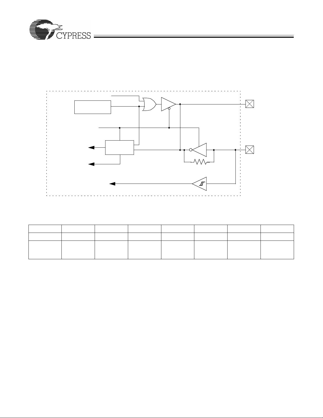
The chip can be clocked from either the internal on-chip clock, or from an oscillator based on an ex ternal resonator/crystal, as
shown in
Configuration Register,
Figure 9-1
Clk2x (12 MHz)
(to Microcontroller)
. No addit ional capacitan ce is included on chip at the XTALIN/OUT pins. Oper ati on is controlled by the Clock
Figure 9-2
Int Clk Output Disable
Interna l Osc
Ext Clk Enable
Clk1x (6 MHz)
(to USB SIE)
.
Clock
Doubler
XTALOUT
XTALIN
30 pF
Port 2.1
Figure 9-1. Clock Oscillator On-chip Circui t
7 6 5 4 3 2 1 0
R/W R/W R/W R/W R/W - R/W R/W
Ext. Clock
Resume
Delay
All bits of the Clock Configuration Register reset to 0. Reserved bits must always be written as a 0.
Setting External Oscillator Enable (bit 0) high causes the part to switch to external clock mode, as described in Section 9.1. (If
the bit is already set, writing a ‘1’ again has no effect.) Clearing this bit has no immediate effect, although the state of this bit is
used when waking out of suspend mode to select between internal and external clock. When this bit is cleared XTALIN will be
configured as an input with a weak pull down and can be used as a GPIO input (P2.1).
The Internal Clock Output Disable ( bit 1) can be set to 1 to keep the internal clock from driving out to XTALOUT. If set, XTALOUT
will drive hi gh. Thi s bit has no effect when the external oscillator is enabled.
The Precisi on USB Clocking Enabl e (bit 2) only affects operation in Internal Oscillator M ode. In that mode, this bit mus t be set to
1 to cause t he internal c lo ck t o a utomati call y preci se ly tu ne to USB t iming r equir ement s (6 M Hz ±1. 5%). The f requ ency m ay ha v e
a looser initia l to lerance at power-up, but all USB transmissions from the chip wil l meet the USB specification.
The Low Voltage Reset Disable (bit 3) disables the LVR circuit when set to 1. See Section 10.1.
The Wake-up Timer Adjust Bits (bit s 6:4) are used to adjust the Wake-up timer period, as descri bed in Section 11.2.
The Resume Delay (bit 7) selects the delay time when switching to the external oscillator, or when waking from suspend mode
with the e xternal oscil lator enab led. The del ay is 128 µs when this bit is 0, and 4 ms when this bit is 1. The sho rter time is adequat e
for operation with ceramic re sonators, while the long er ti m e is preferred for start-up with a crystal. (These times
an initial osci llator st art-up time which depends on t he resonatin g element. This ti me is typicall y 50–100 µs for ce ramic r esonators
and 1–10 ms for crystals). When waking from suspend mode with the internal osci llator , t he delay time is only 8 µs in addition to
a delay of appr oximately 1 µs for the oscillator to start.
Wake-up
Timer Adjust
Bit 2
Wake-up
Timer Adjust
Bit 1
Figure 9-2. Clock Configuration Register (Address 0xF8)
Wake-up
Timer Adjust
Bit 0
Low Voltage
Reset
Disable
Precision
USB Clocking
Enable
Internal Clock
Output
Disable
External
Oscillator
Enable
do not include
14

FOR
FOR
enCoRe™
USB CY7C63722/23
PRELIMINARY
CY7C63742/43
9.1 Internal / External Oscillator Operation
The internal oscillator provi des an operating clock, factory set to a nominal frequency of 6 MHz. This clock requires no external
components . At power-up, the chip operates from the internal c lock. In this mode, t he internal clock is b uffered and driven to the
XTALOUT pin by default, and the state of the XTALIN Pin can be read at Port 2.1. While the internal clock is enabled, its output
can be disable d at the XTALOUT pin by setting the Internal Clock Output Disable bit of the Clock Confi guration Register.
Setting bit 0 o f the Cl oc k Confi gura tion Reg ister disab l es the i nternal cloc k, and ha lts t he pa rt while the e x ternal resona tor/crystal
oscillator is started. The steps involved in switching from Internal to External Cloc k m ode are as follows:
1. At reset, chip begins operation using the internal clock.
2. Firmware sets Bit 0 of the Clock Configuration Register. For example,
mov A, 1h ; Set Bit 0 (External Oscillator Enable); bit 7 cleared gives fas ter start-up
iowr F8h ; Write to Clock Configuration Register
3. Internal clocking is halted, the internal oscillator is disabled, and the external cloc k oscillator is enabled.
4. After the e xternal cloc k bec omes sta ble , ch ip cloc ks are re -enab le d using the e xternal cloc k signal . (Note t hat the tim e for the
external cl ock to become stable depends on the external resonating device; see next section.)
5. After an addition al del ay the CPU i s released to run. This delay depends on the state of the Ext. Clock Resum e Delay bit of
the Clock Configuration Register. The time is 128 µs if the bit is 0, or 4 ms if the bit is 1.
6. Once the chip ha s been set to ext ernal oscill ator , it can only retu rn to internal cloc k when wak ing from sus pend mode. Clearing
bit 0 of the Clock Conf iguration Register will not re-enable internal clock mode until suspend mode is ent ered. See Section
11.0 for more details on suspend mode oper ation.
If the Internal Clock is enabled, the XTALIN pin can serve as a general purpose input, and its state can be read at Port 2, Bit 1
(P2.1) . Refer to
cannot provi de an interrupt source to the CPU .
Figure 12-8
for the Port 2 data register. In this mode, there is a weak pull-down at the XTALIN pin. This input
9.2 External Oscillator
The user can connect a l ow-cost ceramic re sonator or an external osci ll ator to the XTALIN / XTALOUT pins to provi de a precise
reference frequency for the chip clock, as shown in
crystal with external capacitors. To run from the external resonator, Bit 0 o f the Clock Conf iguration Register must be set to 1, as
explained in the previous section.
Start up times for the external oscillator depend on the resonating device. Ceramic resonator based oscillators typically start in
less than 100 µs, while cryst al based oscillators take l onger, typically 1 to 10 ms. Board capacitance s hould be minimized on the
XTALIN and XTALOUT pins by keeping the traces as short as possible.
An external 6 MHz cloc k can be appli ed to the XTALIN pin if the XTALOUT pin is left open.
Figure 9-1
. The ext ernal components required are a ceramic resonator or
10.0 Reset
The USB Controller supports three ty pes of resets. The effects of the reset are listed below. The reset types are:
1. Low Voltage Reset (L VR)
2. B rown Out Res e t (B O R)
3. Watch Dog Reset (WDR)
The occurrence of a reset is recorded in the Processor Status and Control Register (see
record the occurrence of LVR/BOR and WDR respectivel y. The firmware can interrogate these bits to determine the cause of a
reset.
The microcont roller begi ns e xecut ion fro m ROM addr ess 0x00 00 after a LVR, BOR or WDR reset. A lthough t his looks lik e interrupt
vector 0, there is an important difference. Reset processing does NOT push the program counter, carry flag, and zero flag onto
program stack. Attempting to execute either a RET or RETI in the reset handler will cause unpredictable execution results.
The foll owing eve nts take place on reset. More det ails on the various resets are given in the following sections.
1. All registers are reset to their default st ates (all bits cleared, except in Processor Status and Control Register).
2. GPIO and USB pins are set to high-impedance state.
3. The VREG pin is set to high-impe dance state.
4. Interrupts are disabled.
5. USB operation is disabled and must be enabl ed by fi rmware if desired, as explained in Section 14.1 .
6. For a BOR or LVR, the external oscil lator is disab led and Internal Clo ck mode is acti vated, follo wed by a t ime-out period t
for V
to stabilize . A WDR does not change the cloc k mode , and there is no dela y for VCC stabilizati on on a WDR. Note that
CC
Figure 20-1
). Bits 4 and 6 are used to
START
15
 Loading...