

CYPRESS CY7C63722, CY7C63723, CY7C63743 User Manual

CY7C63722
CY7C63723
CY7C63743
enCoRe™ USB Combination Low-Speed
USB and PS/2 Peripheral Controller
1.0 Features
• enCoRe™ USB - enhanced Component Reduction
—Internal oscillator e liminates the need for an external
crystal or resonator
—Interface can auto-configure to operate as PS/2 or
USB without the need for external components to
switch between modes (no General Purpose I/O
[GPIO] pins needed to manage dual mode cap ability)
—Internal 3.3V regulator for USB pull-up resistor
—Configurable GPIO for real-world interface without
external components
• Flexible, cost-effective solution for applications that
combine PS/2 and low-speed USB, such as mice, gamepads, joysticks, and many others.
• USB Specification Compliance
—Conforms to USB Specification, Version 2.0
—Conforms to USB HID Specification, Version 1.1
—Supports one low-speed USB device address and
three data endpoints
—Integrated USB transceiver
—3.3V regulated output for USB pull-up resistor
• 8-bit RISC microcontroller
—Harvard architecture
—6-MHz external ceramic resonator or internal clock
mode
—12-MHz internal CPU clock
—Internal memory
—256 bytes of RAM
—8 Kbytes of EPROM
—Interface can auto-configure to operate as PS/2 or
USB
—No external componen ts for switching betw een PS/2
and USB modes
—No GPIO pins needed to manage dual mode
capability
• I/O ports
—Up to 16 versatile GPIO pins, individually
configurable
—High current drive on any GPIO pin: 50 mA/pin
current sink
—Each GPIO pin supports high-impedance inputs,
internal pull-ups, open drain outputs or traditional
CMOS outputs
—Maskable interrupts on all I/O pins
• SPI serial communication block
—Master or slave operation
—2 Mbit/s transfers
• Four 8-bit Input Capture registers
—Two registers each for two input pins
—Capture timer setting with five prescaler settings
—Separate registers fo r rising and falling edge capture
—Simplifies interface to RF inputs for wireless
applications
• Internal low-power wake-up timer during suspend
mode
—Periodic wake-up with no external components
• Optional 6-MHz internal oscillator mode
—Allows fast start-up from suspend mode
• Watchdog Reset (WDR)
• Low-voltage Reset at 3.75V
• Internal brown-out reset for suspend mode
• Improved output drivers to reduce EMI
• Operating voltage from 4.0V to 5.5VDC
• Operating temperature from 0°C to 70°C
• CY7C63723 available in 18-pin SOIC, 18-pin PDIP
• CY7C63743 available in 24-pin SOIC, 24-pin PDIP , 24-pin
QSOP
• CY7C63722 available in DIE form
• Industry standard programmer support
Cypress Semiconductor Corporation • 3901 North First Street • San Jose • CA 95134 • 408-943-2600
Document #: 38-08022 Rev. *B Revised September 27, 2004
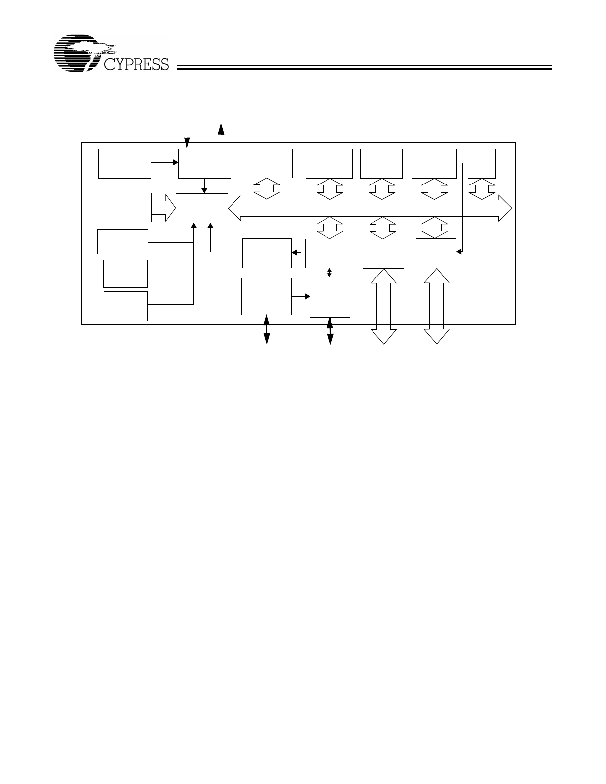
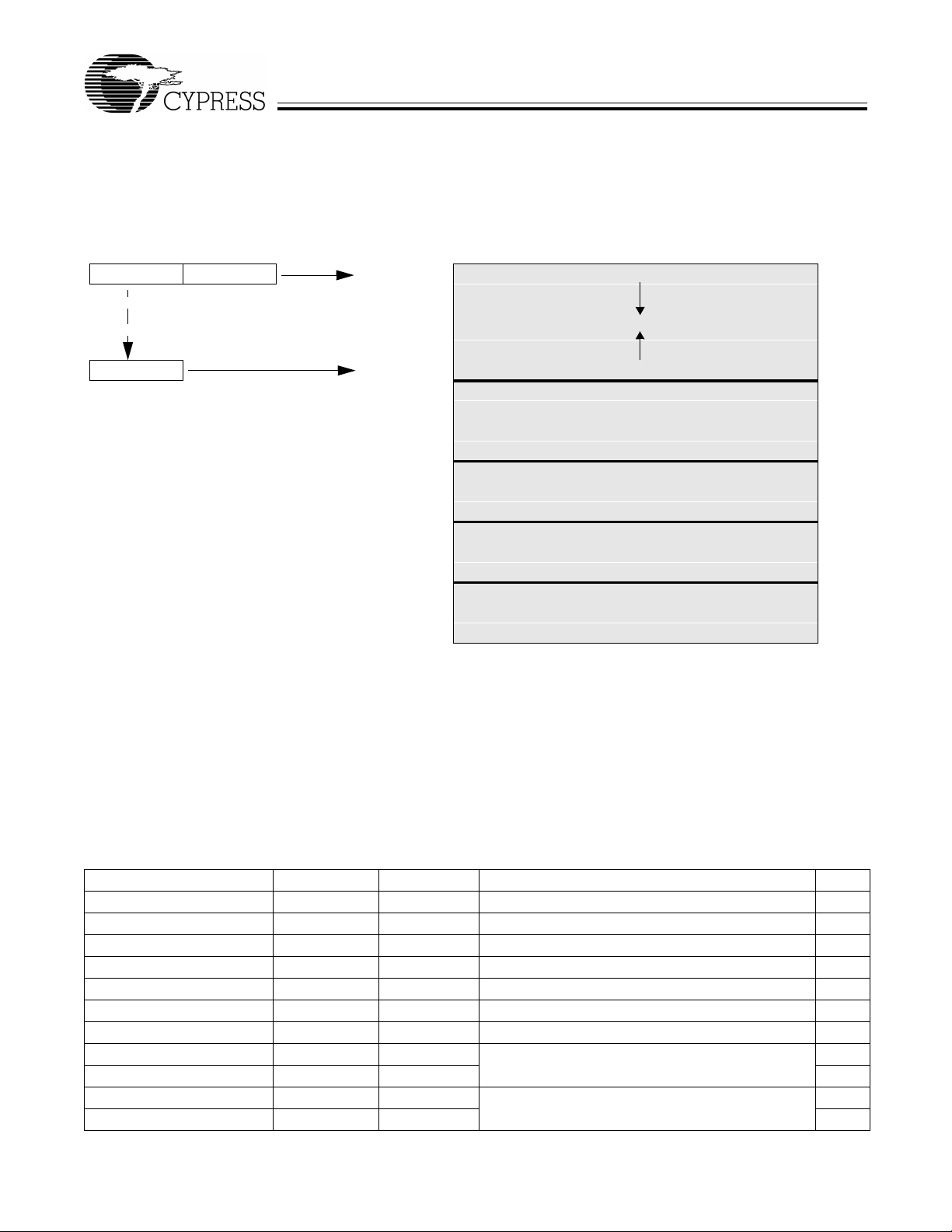
2.0 Logic Block Diagram
FOR
FOR
CY7C63722
CY7C63723
CY7C63743
XTALOUT XTALIN/P2.1
Internal
Oscillator
EPROM
8K Byte
Brown-out
Reset
Xtal
Oscillator
8-bit
RISC
Core
Wake-Up
Timer
Interrupt
Controller
Watch
Dog
Timer
Low
Voltage
Reset
3.3V
Regulator
VREG/P2.0
3.0 Functional Overview
3.1 enCoRe USB—The New USB Standard
Cypress has reinvented its leadership position in the
low-speed USB market with a new family of innovative
microcontrollers. Introducing...enCoRe USB—“enhanced
Component Reduction.” Cypress has leveraged its design
expertise in USB solutions to create a new family of low-speed
USB microcontrollers that enables peripheral developers to
design new prod ucts with a minimum number of compone nt s .
At the heart of the enCoRe USB technology is the breakthrough de sign of a crystalless os cillator. By integrating t he
oscillator into our chip, an external crystal or resonator is no
longer needed. We have also integrated other extern al components common ly found in low-sp eed USB applica tions such as
pull-up resistors , wake-up ci rcuitry, and a 3.3V regul ator. All of
this adds up to a lower system cost.
The CY7C637xx is an 8-bit RISC one-time-programmable
(OTP) microcontroller. The instructi on set has been opt imize d
specifically for USB and PS/2 operati ons , alt hou gh the mic rocontrollers can b e us ed fo r a v ari ety o f other embedded a ppl ications.
The CY7C637xx features up to 16 G PIO pins to support USB,
PS/2 and other applications . The I/O pins are grouped into two
ports (Port 0 to 1) where each pin can be individually
configured as input s with internal p ull-up s, open drai n output s,
or traditional CMOS output s with programm able drive strength
of up to 50 mA output drive. Additionally, each I/O pin can be
used to generate a GPIO i nter rupt to the mi croco ntrolle r. Note
the GPIO interrupts all share the same “GPIO” interrup t vector .
The CY7C637xx mic rocontrollers fe ature an interna l oscillator .
With the presence of USB traf fic, the int erna l oscilla tor can be
set to precisely tune to USB timing requirements (6 MHz
RAM
256 Byte
USB
Engine
12-bit
Timer
Port 1
GPIO
Capture
Timers
Port 0
GPIO
SPI
USB &
PS/2
Xcvr
D+,D–
±1.5%). Optionally, an external 6-MHz ceramic resonator can
be used to provide a higher precision reference for USB
operation. This clock generator reduces the clock-related
noise emissions (EMI). The clock generator provides the 6and 12-MHz clocks that rem ain internal to the mic rocontroller .
The CY7C637xx has 8 Kbytes of EPROM and 256 bytes of
data RAM for stack space, user variables, and USB FIFOs.
These parts i nclude low- voltage re set logic, a W atchd og timer ,
a vectored interrupt controll er, a 12-bit free-runnin g timer, and
capture timers. The low-voltage reset (LVR) logic detects
when power is applied to the device, resets the logic to a
known state, and begins executing instructions at EPROM
address 0x0000. LVR will also reset the part when V
below the operating voltage range. The Watchdog timer can
be used to ensure the firmware never gets stalled for more
than approximately 8 ms.
The microcontroller supports 10 maskable interrupts in the
vectored interrupt c ontroller . Interrupt sour ces include the U SB
Bus-Reset, the 128-µs and 1.024-ms outputs from the
free-running timer, three USB endpoints, two capture timers,
an internal wake-up tim er and th e G PIO p ort s . The timers bits
cause periodic interrupts when enabled. The USB endpoints
interrupt after USB transactions complete on the bus. The
capture timers interrupt whenever a new timer value is saved
due to a selected GPIO edge event. The GPIO ports have a
level of masking to select which GPIO inputs can cause a
GPIO interrupt. For additional flexibility, the input transition
polarity that causes an interrupt is programmable for each
GPIO pin. The interrupt polarity can be either rising or falling
edge.
The free-running 12-bit timer clocked at 1 MHz provides two
interrupt sources a s no ted above (128 µs and 1.024 ms ). Th e
timer can be used to measure the duration of an event under
firmware control by read ing the timer at the start and end of an
P1.0–P1.7
P0.0–P0.7
CC
drops
Document #: 38-08022 Rev. *B Page 2 of 49
FOR
FOR
CY7C63722
CY7C63723
CY7C63743
event, and subtracti ng the two values. T he four capture ti mers
save a programmable 8 bit range of the free-running timer
when a GPIO edge occurs on the two capture pins (P0.0,
P0.1).
The CY7C637xx includes an integrated USB serial interface
engine (SIE) that supports the integrated peripherals. The
hardware supports one USB device address with three
endpoints. The SIE al low s the USB hos t to c ommun ic ate with
the function integrated into the microcontroller. A 3.3V
The USB D+ and D– USB pins c an alternately be used a s PS/2
SCLK and SDATA signals, so that products can be designed
to respond to either USB or PS/2 modes of operation. PS/2
operation is suppo rted with i nte rnal pu ll-u p res is tors on SC LK
and SDAT A, the abil ity to di sable the regul ator outp ut pin, an d
an interrupt to signal the start of PS/2 activity. No external
components are necessary for dual USB and PS/2 systems,
and no GPIO pins need to b e dedicated to switching b etween
modes. Slow edge rates operate in both modes to reduce EM I.
regulated output pin provides a pull-up source for the external
USB resistor on the D– pin.
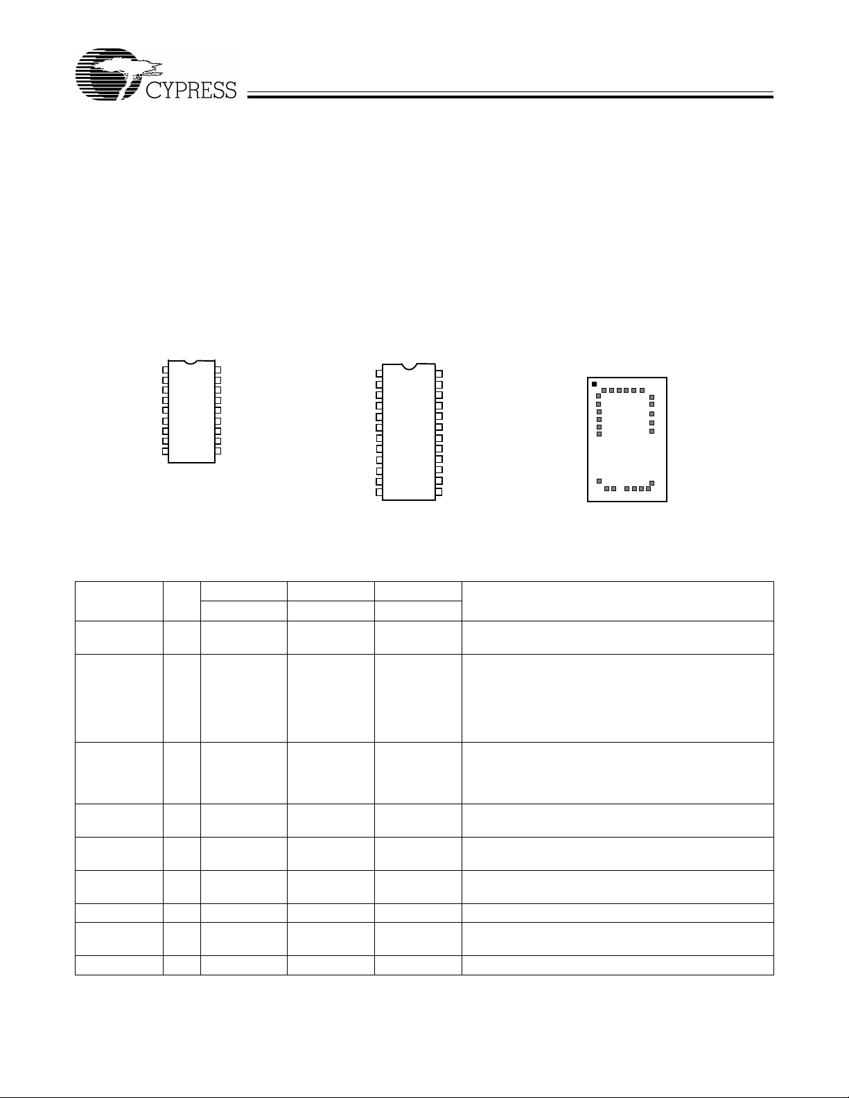
4.0 Pin Configurations
Top View
CY7C63723
18-pin SOIC/PDIP
P0.0
1
P0.1
2
P0.2
3
P0.3
4
P1.0
5
6
VSS
7
VPP
VREG/P2.0
XTALIN/P2.1
8
9
18
17
16
15
14
13
12
11
10
P0.4
P0.5
P0.6
P0.7
P1.1
D+/SCLK
D–/SDATA
VCC
XTALOUT
CY7C63743
24-pin SOIC/PDIP/QSOP
P0.0
1
P0.1
P0.2
P0.3
P1.0
P1.2
P1.4
P1.6
VSS
VPP
VREG/P2.0
XTALIN/P2.1
24
23
2
22
3
21
4
20
5
19
6
18
7
17
8
16
9
15
10
14
11
13
12
P0.4
P0.5
P0.6
P0.7
P1.1
P1.3
P1.5
P1.7
D+/SCLK
D–/SDATA
VCC
XTALOUT
CY7C63722-XC
3 P0.2
2 P0.1
P0.3
4
P1.0
5
6
P1.2
P1.4
7
P1.6
8
9
VSS
VSS
10
111213
VPP
VREG
DIE
1 P0.0
25 P0.4
24 P0.5
23 P0.6
22
P0.7
21
P1.1
20
P1.3
19
P1.5
18
P1.7
17
D+/SCLK
15
16
14
VCC
D-/SDATA
XTALOUT
XTALIN/P2.1
5.0 Pin Definitions
CY7C63723 CY7C63743 CY7C63722
Name I/O
D–/SDATA,
D+/SCLK
P0[7:0] I/O 1, 2, 3, 4,
I/O 12
13
15, 16, 17, 18
15
16
1, 2, 3, 4,
21, 22, 23, 24
16
17
1, 2, 3, 4,
22, 23, 24, 25
USB differential data lines (D– and D+), or PS/2 clock
and data signals (SDATA and SCLK)
GPIO Port 0 capable of sinking up to 50 mA/pin, or
sinking controlled low or high programmable current.
Can also source 2 mA current, provide a resistive
pull-up, or serve as a high-impedance input. P0.0 and
P0.1 provide inputs to Capture Timers A and B, respectively.
P1[7:0] I/O 5, 14 5, 6, 7, 8,
17, 18, 19, 20
5, 6, 7, 8,
18, 19, 20, 21
IO Port 1 capable of sinking up to 50 mA/pin, or sinking
controlled low or high programma ble c urrent. Can also
source 2 mA current, provide a resistive pull-up, or
serve as a high-impedance input.
XTALIN/P2.1 IN 9 12 13 6-MHz ceramic resonator or external clock input, or
P2.1 input
XT ALOUT OUT 10 13 14 6-MHz ceramic resonator return pi n or internal oscillator
output
V
PP
V
CC
7 10 11 Programming voltage supply, ground for normal
operation
11 14 15 Voltage supply
VREG/P2.0 8 11 12 Voltage supply for 1.3-kΩ USB pull-up resistor (3.3V
nominal). Also serves as P2.0 input.
V
SS
6 9 9, 10 Ground
Description18-Pin 24-Pin 25-Pad
Document #: 38-08022 Rev. *B Page 3 of 49

FOR
FOR
CY7C63722
CY7C63723
CY7C63743
6.0 Programming Model
Refer to the CYASM Assembler User’s Guide for more deta ils
on firmware operation with the CY7C637xx microcontrollers.
6.1 Program Counter (PC)
The 14-bit program counter (PC) allows access for up to 8
Kbytes of EPROM using the CY7C637xx architecture. The
program counter is cleared during reset, such that the first
instruction executed after a reset is at address 0x0000. This
instruction is typica lly a jump inst ruction to a reset h andler that
initializes the appli cat ion.
The lower 8 bits of the program counter are incremented as
instructions are l oaded and exec uted. The upper six bit s of the
program counter are incremented by executing an XPAGE
instruction. As a result, th e last instr uction exec uted within a
256-byte “page” of sequential code should be an XPAGE
instruction. The assembler directive “XPAGEON” will cause
the assembler to insert XPAGE instructions automatically. As
instructions can be eit her one or two bytes long, the assembl er
may occasionally need to inser t a NOP followe d by an XP AGE
for correct execution.
The program counter of the next instruction to be executed,
carry flag, and zero flag are saved as two bytes on the progra m
stack during an interrupt acknowledge or a CALL instruction.
The program counter, carry flag, and zero flag are restored
from the program stack only during a RETI instruction.
Please note the program counte r cannot be acces sed directl y
by the firmware. The program stack can be examined by
reading SRAM from location 0x00 and up.
6.2 8-bit Accumulator (A)
The accumulator is the general-purpose, do everything
register in the architecture where results are usually calculated.
6.3 8-bit Index Register (X)
The index register “X” is available to the firmware as an
auxiliary accumu lator . The X register also allows the proce ssor
to perform indexed operations by loading an index value
into X.
The return from interrupt (RETI) instruction decrements the
program stack pointer, then restores the second byte from
memory addressed by the PSP. The program stack pointer is
decremented again and th e first byte is restored from mem ory
addressed by the PSP. After the program counter and flags
have been restored from st ack, the interrupt s are enabled. The
effect is to restore the program counter and flags from the
program stack, decrement the program stack pointer by two,
and reenable interrupts.
The call subroutine (CALL) instruction stores the program
counter and flags on the program stack and increments the
PSP by two.
The return from subroutine (RET) instruction restores the
program counter, but not the flags, from program stack and
decrements the PSP by two.
Note that there are restrictions in using the JMP, CALL, and
INDEX instructions across the 4-KByte boundary of the
program memory. Refer to the CYASM Assembler User’s
Guide for a detailed description.
6.5 8-bit Data Stack Pointer (DSP)
The data stack pointer (DSP) supports PUSH and POP
instructions that use the data stack for temporary storage. A
PUSH instruction will pre-decrement the DSP, then write data
to the memory location addressed by the DSP. A POP
instruction will read dat a from the me mory lo catio n addres sed
by the DSP, then post-increment the DSP.
During a reset, the Data Stack Pointer will be set to zero. A
PUSH instruction when DSP equ als ze ro will wri te da t a at th e
top of the data RAM (address 0xFF). This would write data to
the memory area re serv ed f or a FIF O f or U SB e ndpoi nt 0. In
non-USB applications, this works fine and is not a problem.
For USB applications, the firmware should set the DSP to an
appropriate location to avoid a memory conflict with RAM
dedicated to USB FIFOs. The memory requirements for the
USB endpoints are shown in Section 8.2. For example,
assembly instructions to set the DSP to 20h (giving 32 bytes
for program and data stack combined) are shown below.
MOV A,20h ; Move 20 hex into Accumu lator (must be
D8h or less to avoid USB FIFOs)
SWAP A,DSP ; swap acc umula tor value in to DSP reg ist er
6.4 8-bit Program Stack Pointer (PSP)
During a reset, the progra m sta ck point er (PSP) is set to zero.
This means the program “stack” starts at RAM address 0x00
and “grows” upward from there. Note that the program stack
pointer is directly addressable under firmware control, using
the MOV PSP,A instruction. The PSP supports interrupt
service under hardware control and CALL, RET, and RETI
instructions under firmware control.
During an interrupt acknowledge, interrupts are disabled and
the program counter, carry flag, and zero flag are written as
two bytes of data memory. The first byte is stored in the
memory addressed by the program stack pointer, then the
PSP is incremented. The second byte is stored in memory
addressed by the progra m st ack poi nter and the PS P is inc remented again. The net effect is to store the program counter
and flags on the program “stack” and increment the program
stack pointer by two.
Document #: 38-08022 Rev. *B Page 4 of 49
6.6 Address Modes
The CY7C637xx microcontrollers support three addressing
modes for instructions that require dat a operands: dat a, direct,
and indexed.
6.6.1 Data
The “Data” address mode refers to a data operand that is
actually a const ant en coded in t he instruc tion. As an example,
consider the instruction that loads A with the constant 0x30:
• MOV A, 30h
This instruction will require two bytes of code where the first
byte identifies the “MOV A” inst ruc tion w ith a d at a operand as
the second byte. Th e second byte of the instru ction will b e the
constant “0xE8h”. A constant may be referred to by name if a
prior “EQU” statement a ssigns the co nstant valu e to the name.
For example, the following code is equivalent to the example
shown above.
FOR
FOR
CY7C63722
CY7C63723
CY7C63743
• DSPINIT: EQU 30h
• MOV A,DSPINIT
6.6.2 Direct
“Direct” address mode is used when the data operand is a
variable stored in SRAM. In that cas e, the one byte address of
the variable is encoded in the instruction. As an example,
consider an instruction that loads A with the contents of
memory address location 0x10h:
• MOV A, [10h]
In normal usage, variable names are assigned to variable
addresses using “EQU” statements to improve the readability
of the assembler source code. As an example, the following
code is equivalent to the example shown above.
• buttons: EQU 10h
• MOV A, [buttons]
6.6.3 Indexed
“Indexed” address mode allows the firmware to manipulate
arrays of data stored in SRAM. The address of the data
operand is the sum of a constant encoded in the instruction
and the contents of the “X” register. In normal usage, the
constant will be the “base” address of an array of data and the
X register will cont ain an index th at indica tes which element of
the array is actually addressed.
• array: EQU 10h
• MOV X,3
• MOV A, [x+array]
This would have the effect of loading A with the fourth element
of the SRAM “array” that begins at addr ess 0x 10h . The fourth
element would be at address 0x13h.
7.0 Instruction Set Summary
Refer to the CYASM Assembler User’s Guide for detailed
information on these instructions. Note that conditional jump
instructions (i.e., JC, JNC, JZ, JNZ) take five cycles if jump is
taken, four cycles if no jump.
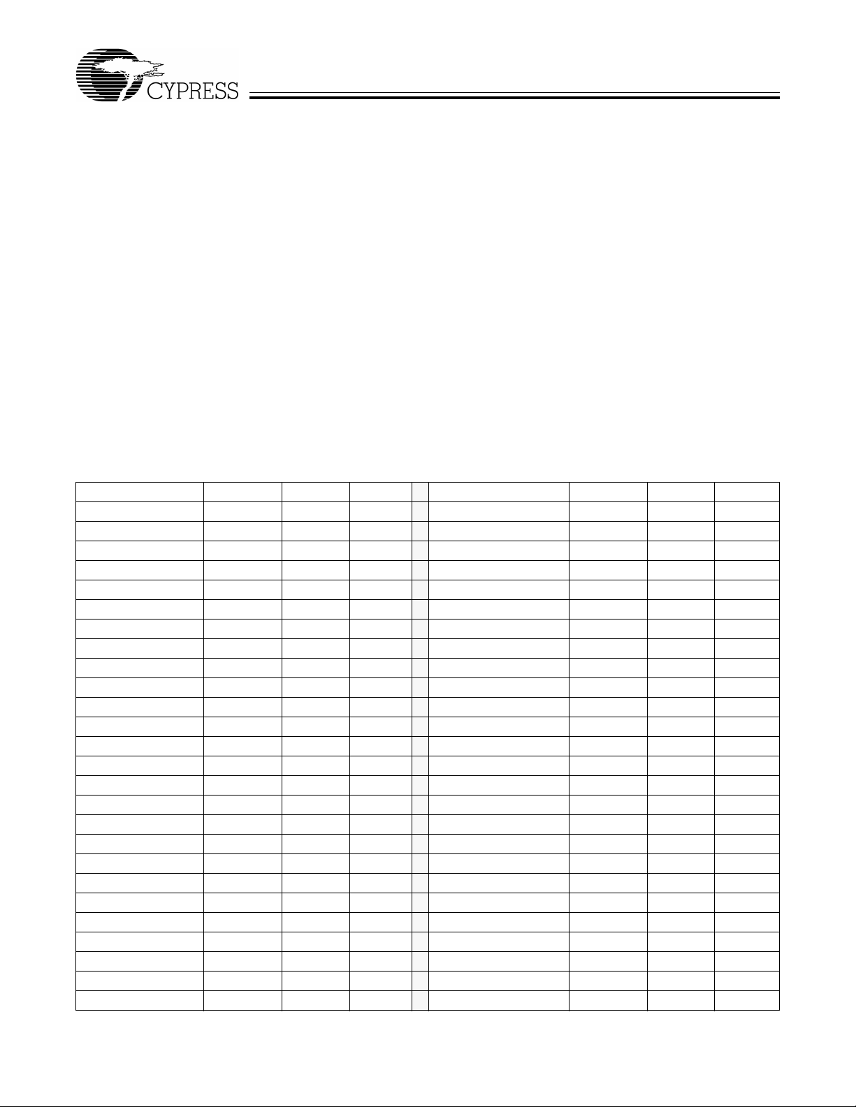
MNEMONIC Operand Opcode Cycles
HALT 00 7
ADD A,expr data 01 4 INC A acc 21 4
ADD A,[expr] direct 02 6
ADD A,[X+expr] index 03 7
ADC A,expr data 04 4 INC [X+expr] index 24 8
ADC A,[expr] direct 05 6
ADC A,[X+expr] index 06 7
SUB A,expr data 07 4 DEC [expr] direct 27 7
SUB A,[expr] direct 08 6
SUB A,[X+expr] index 09 7
SBB A,expr data 0A 4 IOWR expr address 2A 5
SBB A,[expr] direct 0B 6
SBB A,[X+expr] index 0C 7 POP X 2C 4
OR A,expr data 0D 4 PUSH A 2D 5
OR A,[expr] direct 0E 6
OR A,[X+expr] index 0F 7 SWAP A,X 2F 5
AND A,expr data 10 4 SWAP A,DSP 30 5
AND A,[expr] direct 11 6
AND A,[X+expr] index 12 7 MOV [X+expr],A index 32 6
XOR A,expr data 13 4 OR [expr],A direct 33 7
XOR A,[expr] direct 14 6
XOR A,[X+expr] index 15 7 AND [expr],A direct 35 7
CMP A,expr data 16 5 AND [X+expr],A index 36 8
CMP A,[expr] direct 17 7
CMP A,[X+expr] index 18 8 XOR [X+expr],A index 38 8
MOV A,expr data 19 4 IOWX [X+expr] index 39 6
MNEMONIC Operand Opcode Cycles
NOP 20 4
INC X x 22 4
INC [expr] direct 23 7
DEC A acc 25 4
DEC X x 26 4
DEC [X+expr] index 28 8
IORD expr address 29 5
POP A 2B 4
PUSH X 2E 5
MOV [expr],A direct 31 5
OR [X+expr],A index 34 8
XOR [expr],A direct 37 7
Document #: 38-08022 Rev. *B Page 5 of 49

FOR
FOR
CY7C63722
CY7C63723
CY7C63743
MNEMONIC Operand Opcode Cycles
MOV A,[expr] direct 1A 5
MOV A,[X+expr] index 1B 6
MOV X,expr data 1C 4
MOV X,[expr] direct 1D 5
reserved 1E
XPAGE 1F 4
MOV A,X 40 4
MOV X,A 41 4
MOV PSP,A 60 4
CALL addr 50 - 5F 10
JMP addr 80-8F 5
CALL addr 90-9F 10
JZ addr A0-AF 5 (or 4) JACC addr E0-EF 7
JNZ addr B0-BF 5 (or 4)
MNEMONIC Operand Opcode Cycles
CPL 3A 4
ASL 3B 4
ASR 3C 4
RLC 3D 4
RRC 3E 4
RET 3F 8
DI 70 4
EI 72 4
RETI 73 8
JC addr C0-CF 5 (or 4)
JNC addr D0-DF 5 (or 4)
INDEX addr F0-FF 14
Document #: 38-08022 Rev. *B Page 6 of 49
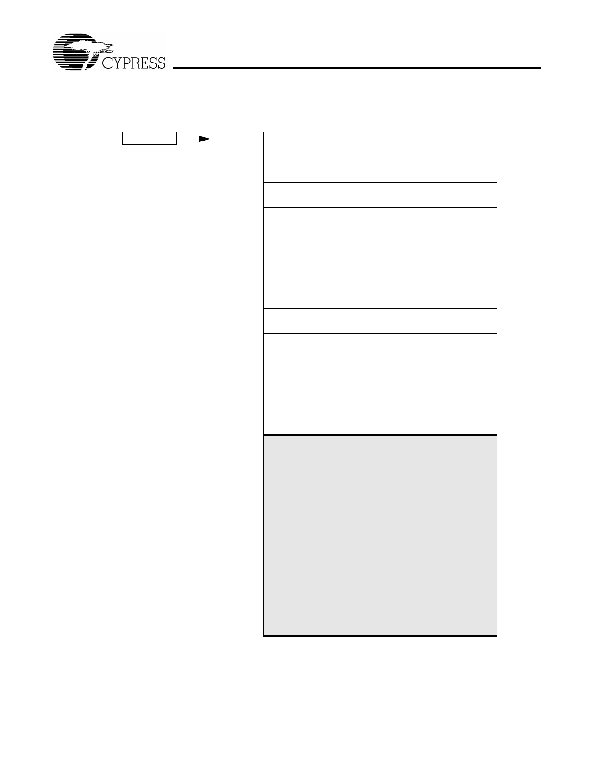
8.0 Memory Organization
FOR
FOR
CY7C63722
CY7C63723
CY7C63743
8.1 Program Memory Organization
After reset Address
14 -bit PC 0x0000 Program execution begins here after a reset
[1]
0x0002 USB Bus Reset interrupt vector
0x0004 128-µs timer interrupt vector
0x0006 1.024-ms timer interrupt vector
0x0008 USB endpoint 0 interrupt vecto r
0x000A USB endpoint 1 interrupt ve ctor
0x000C US B endpoint 2 in terrupt vector
0x000E SPI interrupt vector
0x0010 Capture timer A interrupt Vector
0x0012 Capture timer B interrupt vector
0x0014 GPIO interrupt vector
0x0016 Wake-up interrupt vector
0x0018 Program Memory begins here
0x1FDF 8 KB PROM ends here (8K - 32 bytes). See Note below
Figure 8-1. Program Memory Space with Interrupt Vector Ta ble
Note:
1. The upper 32 bytes of the 8K PROM are reserved. Therefore, the user’s program mus t not overwr i te this spac e.
Document #: 38-08022 Rev. *B Page 7 of 49
FOR
FOR
8.2 Data Memory Organization
The CY7C637xx microcontrollers provide 256 bytes of data
RAM. In normal usage, the SRAM is partitioned into four
areas: program stack, data stack, user variables and USB
endpoint FIFOs as shown below.
After reset Address
8-bit DSP 8-bit PSP 0x00 Program Stack Growth
(User’s firmware moves DSP)
8-bit DSP User Selected Data Stack Growth
User Variables
0xE8
USB FIFO for Address A endpoint 2
CY7C63722
CY7C63723
CY7C63743
0xF0
USB FIFO for Address A endpoint 1
0xF8
USB FIFO for Address A endpoint 0
Top of RAM Memory 0xFF
Figure 8-2. Data Memory Organization
8.3 I/O Register Summary
I/O registers are accessed via the I/O Read (IORD) and I/O
Write (IOWR, IOWX) instructions. IORD reads the selected
port into the accumul ator . IO WR writes data fro m the accum ulator to the selected port. Indexed I/O Write (IOWX) adds the
contents of X to the address in the instru cti on to form the port
address and writes dat a fr om the accu mulato r to the spec ified
Table 8-1. I/O Register Summary
Register Name I/O Address Read/Write Function Fig.
Port 0 Data 0x00 R/W GPIO Port 0 12-2
Port 1 Data 0x01 R/W GPIO Port 1 12-3
Port 2 Data 0x02 R Auxiliary input register for D+, D–, VREG, XTALIN 12-8
Port 0 Interrupt Enable 0x04 W Interrupt enable for pins in Port 0 21-4
Port 1 Interrupt Enable 0x05 W Interrupt enable for pins in Port 1 21-5
Port 0 Interrupt Polarity 0x06 W Interrupt polarity for pins in Port 0 21-6
Port 1 Interrupt Polarity 0x07 W Interrupt polarity for pins in Port 1 21-7
Port 0 Mode0 0x0A W Controls output configuration for Port 0 12-4
Port 0 Mode1 0x0B W 12-5
Port 1 Mode0 0x0C W Controls output configuration for Port 1 12-6
Port 1 Mode1 0x0D W 12-7
port. Note that specifying address 0 with IOWX (e.g., IOWX
0h) means the I/O port is selected solely by the contents of X.
Note: All bits of all registers are cleared to all zeros on
reset, except the Processor Status and Control Register
(Figure 20-1). All register s not liste d are reserved , and shoul d
never be written by firmware. All bits marked as reserved
should always be writte n as 0 and be tre ate d as unde fin ed by
reads.
Document #: 38-08022 Rev. *B Page 8 of 49

FOR
FOR
CY7C63722
CY7C63723
CY7C63743
Table 8-1. I/O Register Summary (continued)
Register Name I/O Address Read/Write Function Fig.
USB Device Address 0x10 R/W USB Device Address register 14-1
EP0 Counter Register 0x11 R/W USB Endpoint 0 counter register 14-4
EP0 Mode Register 0x12 R/W USB Endpoint 0 configuration register 14-2
EP1 Counter Register 0x13 R/W USB Endpoint 1 counter register 14-4
EP1 Mode Register 0x14 R/W USB Endpoint 1 configuration register 14-3
EP2 Counter Register 0x15 R/W USB Endpoint 2 counter register 14-4
EP2 Mode Register 0x16 R/W USB Endpoint 2 configuration register 14-3
USB Status & Control 0x1F R/W USB status and control register 13-1
Global Interrupt Enable 0x20 R/W Global interrupt enable register 21-1
Endpoint Interrupt Enable 0x21 R/W USB endpoint interrupt enables 21-2
Timer (LSB) 0x24 R Lower 8 bits of free-running timer (1 MHz) 18-1
Timer (MSB) 0x25 R Upper 4 bits of free-running timer 18-2
WDR Clear 0x26 W Watchdog Reset clear -
Capture Timer A Rising 0x40 R Rising edge Capture Timer A data register 19-2
Capture Timer A Falling 0x41 R Falling edge Capture Timer A data register 19-3
Capture Timer B Rising 0x42 R Rising edge Capture Timer B data register 19-4
Capture Timer B Falling 0x43 R Falling edge Capture Timer B data register 19-5
Capture TImer Configuration 0x44 R/W Capture Timer configuration register 19-7
Capture Timer Status 0x45 R Capture Timer status register 19-6
SPI Data 0x60 R/W SPI read and write data register 17-2
SPI Control 0x61 R/W SPI status and control register 17-3
Clock Configuration 0xF8 R/W Internal / External Clock configuration register 9-2
Processor Status & Control 0xFF R/W Processor status and control 20-1
Document #: 38-08022 Rev. *B Page 9 of 49
FOR
FOR
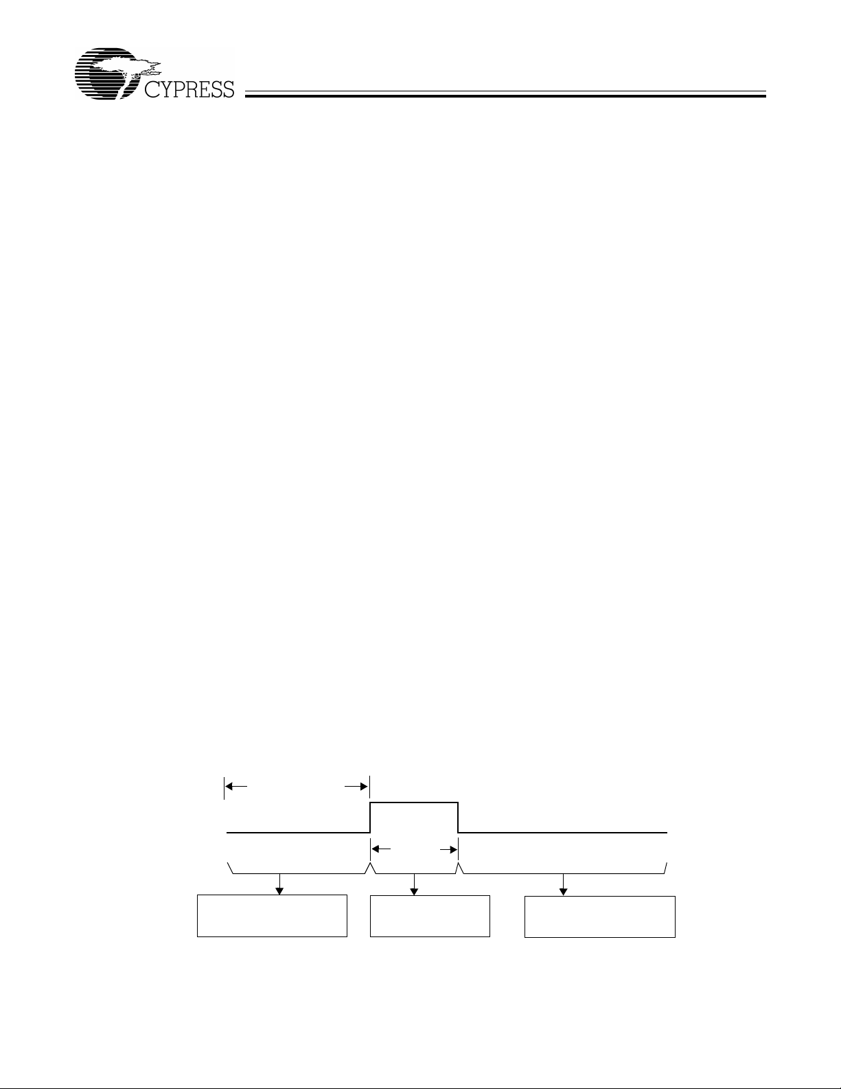
9.0 Clocking
The chip can be c locked f rom eithe r the i nternal on -chip cl ock,
or from an oscilla tor based on an external reso nator/crystal , as
shown in Figure 9-1. No additional capaci t an ce is included on
chip at the XTALIN/OUT pins. Operation is controlled by the
Clock Configuration Register, Figure 9-2.
Int Clk Output Disable
Internal Osc
Ext Clk Enable
CY7C63722
CY7C63723
CY7C63743
XTALOUT
Clk2x (12 MHz)
(to Microcontroller)
Clock
Doubler
XTALIN
Clk1x (6 MHz)
(to USB SIE)
Port 2.1
Figure 9-1. Clock Oscillator On-chip Circuit
Bit # 76543210
Bit Name Ext. Clock
Resume
Delay
Wake-up Timer Adjust Bit [2:0] Low-voltage
Reset
Disable
Precision
USB
Clocking
Enable
Internal
Clock
Output
Disable
External
Oscillator
Enable
Read/Write R/W R/W R/W R/W R/W R/W R/W R/W
Reset 00000000
Figure 9-2. Clock Configuration Register (Address 0xF8)
Bit 7: Ext. Clock Resume Delay
External Clock Resume Delay bit selects the delay time
when switching to the external oscillator from the internal
oscillator mode, or when waking from suspend mode with
the external oscillator enabled.
1 = 4 ms delay.
0 = 128 µs delay.
The delay gives the oscillator time to start up. The shorter
time is adequate for operation with ceramic resonators,
while the longer time i s preferre d for sta rt-up with a crys ta l.
(These times do not include an initial oscillator start-up
time which depends on the resonating element. This time
Bit [6:4]: Wake-up Timer Adjust Bit [2:0]
The Wake-up Timer Adjust Bits are used to adjust the
Wake-up timer period.
If the Wake-up interrupt is enabled in the Global Interrupt
Enable Register, the microc ontro ll er wi ll generate wake-up
interrupts periodically. The frequency of these periodical
wake-up interrupts is adjuste d by setting the Wake-up T imer Adjust Bit [2:0], as described in Section 11.2. One common use of the wake-up inte rrupts is to generate peri odical
wake-up events during suspend mode to check for changes, such as looking for movement in a mouse, while maintaining a low average power.
is typically 50–100 µs for ceramic resonators and 1–10 ms
for crystals). Note that th is bit only select s the delay time for
the external clock mode. When waking from suspend mode
with the internal oscillator (Bit 0 is LOW), the delay time is
only 8 µs in addition to a delay of app roximately 1 µs for the
oscillator to start.
Bit 3: Low-voltage Reset Disable
When V
ue of V
the microcontroller enters a partial suspend state for a period of t
Program execution begins from address 0x0000 after this
t
START
drops below V
CC
) and the Low-voltage Reset circuit is enabled,
LVR
(see Section 26 .0 for the value of t
START
delay period. This prov ide s ti me fo r VCC to stabilize
(see Section 25. 0 f or t he va l-
LVR
START
).
Document #: 38-08022 Rev. *B Page 10 of 49

FOR
FOR
CY7C63722
CY7C63723
CY7C63743
before th e part ex ecut es code . Se e S ectio n 1 0.1 fo r mor e
details.
1 = Disables the LVR circuit.
0 = Enables t he LVR circuit.
Bit 2: Precision USB Clocking Enable
The Precision USB Clocking Enable only affects operation
in internal oscillator m od e. In tha t mode , this bit mus t be
set to 1 to cause the internal clock to au tomatically precisely tune to USB timing requirement s (6 M Hz ± 1.5% ).
The frequen cy may have a l ooser initia l tol eranc e at po wer-up, but all USB trans missions from t he ch ip will meet th e
USB specification.
1 = Enabled. The internal clock accuracy is 6 MHz ±1.5%
after USB traffic is received.
0 = Disabled. The internal clock accuracy is 6 MHz ±5%.
Bit 1: Internal Clock Output Disable
The Internal Clock Output Dis able is used to keep the int ernal clock from driving out to the XTALOUT pin. This bit has
no effect in the external oscillator mode.
1 = Disable int ernal clock out put. XTALOUT pin will drive
HIGH.
0 = Enable the internal clock output. The internal clock is
driven out to the XTALOUT pin.
Bit 0: External Oscillator Enable
At power-up, the chip operates from the internal clock by
default. Setting the Exte rnal Oscillato r Enable bit HIGH disables the internal clock, and halt s the part while the external
resonator/crystal oscillator is started. Clearing this bit has
no immediate effect, although the state of this bit is used
when waking out of su spend mod e to select be tween internal and external clock. In internal clock mode, XTALIN pin
will be confi gured as an i nput with a we ak pull-dow n and
can be used as a GPIO input (P2.1).
1 = Enable the external oscillator. The clock is switched to
external clock mode, as described in Section 9.1.
0 = Enable the internal oscillator.
9.1 Internal/External Oscillator Opera ti on
The internal oscillat or pro vi des an ope rati ng c lo ck , fac tory set
to a nominal frequency of 6 MHz. This clock requires no
external componen ts. At power-up, th e chip operates from the
internal clock. In this mode, the internal clock is buffered and
driven to the XTALOUT pin by default, and the state of the
XT ALIN pin ca n be read at Port 2.1 . While the inte rnal cl ock i s
enabled, its output can be disabled at the XTALOUT pin by
setting the Internal Clock Output Disable bit of the Clock
Configurat ion Register.
Setting the External Oscillator Enable bit of the Clock Configuration Register HIGH disables the internal clock, and halts
the part while the external resonator/crystal oscillator is
started. The steps involved in switching from Internal to
External Clock mode are as follows:
1. At reset, chip begins operation using the internal clock.
2. Firmware sets Bit 0 of the Clock Configuration R egister. For
example,
mov A, 1h ; Set Bit 0 HIGH (External Oscil-
lator Enable bit). Bit 7 cleared
gives faster start-up
iowr F8h ; Write to Clock Configuration
Register
3. Internal clocking is halted, the internal oscillator is disabled,
and the external clock oscillator is enabled.
4. After the external clock becomes stable, chip clocks are
re-enabled using the external clock signal. (Note that the
time for the externa l clock to become st able depends on the
external resonating device; see next sect ion.)
5. After an additional delay the CPU is released to run. This
delay depends on the state of the Ext. Clock Res ume Delay
bit of the Clock Configu r ati on Register. The time is 128 µs
if the bit is 0, or 4 ms if the bit is 1.
6. Once the chip has been set to external osc illator , it can only
return to internal clock when waking from suspend mode.
Clearing bit 0 of the Clock Configuration Register will not
re-enable internal clock mode until suspend mode is
entered. See Section 11.0 for more details on suspend
mode operation.
If the Internal Clock is enabled, the XTALIN pin can serve as
a general purpose input, and its state can be read at Port 2,
Bit 1 (P2.1). Refer to Figure 12-8 for the Port 2 Data Register.
In this mode, there is a weak pull-down at the XTALIN pin. This
input cannot provide an interrupt source to the CPU.
9.2 External Oscillator
The user can connect a low-cost ceramic resonator or an
external oscillator to the XTALIN/XTALOUT pins to provide a
precise reference frequency for the chip clock, as shown in
Figure 9-1. The external components required are a ceramic
resonator or crystal and any associated capacitors. To run
from the external resonator, the External Oscillator Enable bit
of the Clock Configuration Register must be set to 1, as
explained in the previous section.
Start-up times for the external oscillator depend on the
resonating device. Ceramic resonator based oscillators
typically start in less than 100 µs, while crystal based oscillators take longer, typically 1 to 10 ms. Board capacitance
should be minimized on the XTALIN and XTALOUT pins by
keeping the traces as short as possible.
An external 6-MHz clock can be applied to the XTALIN pin if
the XTALOUT pin is left open.
10.0 Reset
The USB Controller supports three types of resets. The effects
of the reset are listed below. The reset types are:
1. Low-voltage Reset (L VR)
2. Brown Out Reset (BOR)
3. Watchdog Reset (WDR)
The occurrence of a re se t is rec ord ed in the Proc es so r Status
and Control Register (Figure 20-1). Bits 4 (Low-voltage or
Brown-out Reset bit) and 6 (Watchdog Reset bit) are used to
record the occurrence of LVR/BOR and WDR respectively.
The firmware can i nterrogate these bit s to determine the cause
of a reset.
Document #: 38-08022 Rev. *B P age 11 of 49
FOR
FOR
CY7C63722
CY7C63723
CY7C63743
The microcontroller begins execution from ROM address
0x0000 after a LVR, BOR, or WDR reset. Although this looks
like interrupt vector 0, there is an important difference. Reset
processing does NOT push th e program count er, carry flag,
and zero flag onto program stack. Attem pting to execute eith er
a RET or RETI in the reset handler will cause unpredictable
execution results.
The following events take place on reset. More details on the
various resets are given in the following sections.
1. All registers are reset to their default states (a ll bits cleared,
except in Processor Status and Control Register).
2. GPIO and USB pins are set to high-impedance state.
3. The VREG pi n is set to high-impedance state.
4. Interrupts are disabled.
5. USB operation is disabled and must be enable d by firmware
if desired, as explained in Section 14.1.
6. For a BOR or LVR, the external oscillator is disabled and
Internal Clock mode is activ ated , follo w ed by a time -out
period t
the clock mode, and there is no delay fo r V
on a WDR. Note that th e Ex tern al Os ci ll ator Enable (Bit 0,
for VCC to stabilize. A WDR does not ch ange
START
CC
stabilization
Figure 9-2) will be cleared by a WDR, but it does not take
effect until suspend mode is entered.
7. The Program Stack Pointer (PSP) and Data Stack Pointer
(DSP) reset to address 0x00. Firmware should move the
DSP for USB applications, as explained in Section 6.5.
8. Program execution beg ins at address 0x0000 after the
appropriate time-out period.
10.1 Low-voltage Reset (LVR)
When V
started and the Low-voltage Reset is initially enabled by
default. At the point where V
Section 25.0 for the value of V
counting for a period of t
of t
START
a partial sus pend state to wait fo r V
begins executing code from address 0x0000.
As long as the LVR circuit is enabled, this reset sequence
repeats wheneve r the V
LVR can be disabled by firmware by setting the Low-voltage
is first applied to the chip, the internal oscillator is
CC
has risen above V
). During this t
CC
), an internal counter starts
LVR
(see Section 26.0 for the value
START
time, the microcontroller enters
START
pin voltage drops below V
CC
to stabilize before it
CC
LVR
LVR
(see
. The
Reset Disable bit in the Clock Configuration Register
(Figure 9-2). In addition, the LVR is automatically disabled in
suspend mode to save power. If the LVR was enabled before
entering suspend mode, it becomes active again once the
suspend mode ends.
When L VR is di sabled duri ng normal operati on (i.e., by wri ting
‘0’ to the Low-voltage Reset Disable bit in the Clock Configuration Register), the chip may enter an unknown state if V
drops below V
times during normal operation. If LVR is disabled (i.e., by
. Therefore, LVR should be enabled at all
LVR
CC
firmware or during suspend mode), a secondary low-voltage
monitor, BOR, becomes active, as described in the next
section. The LVR/BOR Reset bit of the Processor Status and
Control Reg ister (Figure 20-1), is set to ‘1’ if either a LVR or
BOR has occurred.
10.2 Brown Out Reset (BOR)
The Brown Out Reset (BOR) circuit is always active and
behaves like the POR. BOR is asserted whenever the V
voltage to the d evice i s below an internally defined t rip volt age
CC
of approximately 2.5V. The BOR re-enables L VR. That is, onc e
drops and trips BOR, the part remains in reset until V
V
CC
rises above V
normal operation resumes, and the microcontroller starts
executing code from address 0x00 after the t
. At that point, the t
LVR
delay occurs befo re
START
START
delay.
CC
In suspend mode, only the BOR detection is active, giving a
reset if V
is suspended and code is not executing, this lower reset
drops below approxi mately 2.5 V. Since the device
CC
voltage is safe for retaining the state of all registers and
memory. Note that in suspend mode, LVR is disabled as
discussed in Section 10.1.
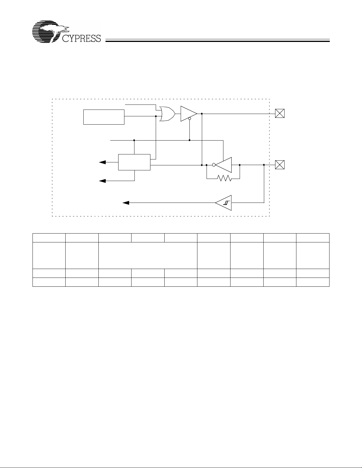
10.3 Watchdog Reset (WDR)
The Watchdog Timer Reset (WDR) occurs when the internal
Watchdog timer rolls over. Writing any value to the write-only
Watchdog Reset R egis ter at add ress 0x 26 will clear t he time r.
The timer will roll over and WDR will occur if it is not cleared
within t
(Watchdog Reset bit) of the Processor Status and Control
Register is set to reco rd th is ev ent (see Section 20.0 for mo re
details). A Watchdog Timer Reset typically lasts for 2–4 ms,
after which the microcontroller begins execution at ROM
address 0x0000.
(see Figure 10-1) of the last clear. Bit 6
WATCH
t
WATCH = 10.1 to
14.6 ms
WDR
(at F
OSC
= 6 MHz)
2–4 ms
At least 10.1 ms
since last write to WDR
WDR goes HIGH
for 2–4 ms
Execution begins at
ROM Address 0x0000
Figure 10-1. Watchdog Reset (WDR, Address 0x26)
Document #: 38-08022 Rev. *B Page 12 of 49

FOR
FOR
CY7C63722
CY7C63723
CY7C63743
11. 0 Suspend Mode
The CY7C637xx parts support a versatile low-po wer s us pen d
mode. In suspend mode, only an enabled interrupt or a LOW
state on the D–/SDA TA pin will wake the part. Two options are
available. For lowest power, all internal circuits can be
disabled, so only an external event will resume operation.
Alternatively, a low- powe r internal wake-up time r ca n be used
to trigger the wake-up interrupt. This timer is described in
Section 11.2, and can be used to periodically poll the system
to check for changes, such as looking for movement in a
mouse, while maintaining a low average power.
The CY7C637xx is pla ced into a low-power st ate by setting the
Suspend bit of the Processor Status and Control Register
(Figure 20-1). All logic blocks in the device are turned off
except the GPIO interrupt logic, the D–/SDATA pin input
receiver, and (optio nally) the w ake-up tim er. The clock oscillators, a s well as th e free-runnin g and Watchdog ti mers are
shut down. Only the occurr ence of an enabled GPIO int errupt,
wake-up interrupt, SPI slave interrupt, or a LOW state on the
D–/SDATA pin will wake the part from suspend (D– LOW
indicates non-idle USB activity). Once one of these resuming
conditions occurs, clocks will be restarted and the device
returns to full operation after the oscillator is stable and the
selected delay period expires. This d elay pe riod is determine d
by selection of internal vs. external clock, and by the state of
the Ext. Clock Resume Delay as explained in Section 9.0.
In suspend mode, any en abled and pending interrup t will wake
the part up. The state of the Interrupt Enable Sense bit (Bit 2,
Figure 20-1) does not have any effect. As a result, any interrupts not inte nded for waking from suspend should be disabled
through the Global Int errupt Enable Register a nd the USB End
Point Interrupt Enable Register (Section 21.0).
If a resuming conditi on e xi st s whe n th e s us pen d bi t is se t, th e
part will still go into suspend and then awake after the appropriate delay time. The Run bit in the Processor Status and
Control Register must be set for the part to resume out of
suspend.
Once the clock is stable and the delay time has expired, the
microcontroller will execute the instruction following the I/O
write that placed the device into suspend mode before
servicing any interrupt requests.
To achieve the lowes t pos si ble curre nt duri ng su spend mode,
all I/O should be held at either V
GPIO bit interrupts (Figure 21-4 and Figure 21-5) should be
disabled for any pins that are not being used for a wake-up
interrupt. This s hould be d one e ven i f the main GPIO Interru pt
Enable (Figure 21-1) is off.
Typical code for entering suspend is shown below:
... ; All GPIO set to low-power st ate (no floating
pins, and bit interrupts disabled unless
using for wake-up)
... ; Enable GPIO and/or wake-up timer
interrupts if desired for wake-up
... ; Select clock mode for wake-up (see
Section 11.1)
mov a, 09h ; Set suspend and run bits
iowr FFh ; Write to Status and Control Register –
Enter suspend, wait for GPIO/wake-up
interru pt or USB activity
nop ; This executes before any ISR
... ; Remaining code for exiting suspend
routine
or ground. In addition, the
CC
11.1 Clocking Mode on Wake-up from Suspend
When exiting suspend on a wake-up event, the device can be
configured to run in either Internal or External Clock mode.
The mode is selected by the state of the External Oscillator
Enable bit in the Clock Configuration Register (Figure 9-2).
Using the I nt e rna l Cl oc k s a ve s t he ex t er nal o sc i ll at o r s tart - up
time and keeps that os cill ator of f for a ddi tional power sa vi ngs.
The external oscillator mode can be activated when desired,
similar to operation at power-up.
The sequence of events for these modes is as follows:
Wake in Internal Clock Mode:
1. Before entering suspend, clear bit 0 of the Clock Configuration Register. This selects Internal clock mode after suspend.
2. Enter suspend mode by setting the suspend bit of the
Processor Status and Control Register.
3. After a wake-up event, the i nternal clock st arts imm ediately
(within 2 µs).
4. A time-out period of 8 µs pas ses, and then firmware
execution begins.
5. At some later point, to activate Exte rnal Clock mode, s et bit
0 of the Clock Configur ation Register . This halts the internal
clocks while the external clock becomes stable. After an
additional time-out (128 µs or 4 ms, see Section 9.0),
firmware execution resumes.
Wake in External Clock Mode:
1. Before entering suspend, the external clock mu st be selected by setting bit 0 o f the Clock Configuration Regi ster. Make
sure this bit is sti ll set when suspend mode is entered. T his
selects External clock mode after suspend.
2. Enter suspend mode by setting the suspend bit of the
Processor Status and Control Register.
3. After a wake-up event, the external oscill ator is started. The
clock is monitored for stability (this takes approximately
50–100 µs with a ceramic resonator).
4. After an additional time-out period (128 µs or 4 ms, see
Section 9.0), firmware execution resumes.
11.2 Wake-up Timer
The wake-up timer runs whenever the wake-up interrupt is
enabled, and is turned off whenever that interrupt is disabled.
Operation is independent of whether the device is in suspend
mode or if the global inter rupt bit is enabled. On ly the Wak e-up
Timer Interrupt Enable bit (Figure 21-1) controls the wake-up
timer.
Once this timer is activated, it will give interrupts after its
time-out period (see below). These in terrupts continue p eriodically until the interrupt is disabled. Whenever the interrupt is
disabled, the wake-up timer is reset, so that a subsequent
enable always results in a full wake-up time.
The wake-up timer can be adjusted by the user through the
Wake-up Timer Adjust bits in the Clock Configuration Register
(Figure 9-2). These bits clear on reset. In addition to allowing
the user to select a range for the wake-up time, a firmware
algorithm can be used to tune out initial pr ocess and o perating
condition variatio ns in this w ake-up time. Thi s can be do ne by
timing the wake-up interrupt time with the accurate 1.024-ms
timer interrupt, and a djusting the T imer Adjus t bits accordin gly
to approximate the desired wake-up time.
Document #: 38-08022 Rev. *B Page 13 of 49
FOR
FOR
Table 11-1. Wake-up Timer Adjust Settings
Adjust Bits [2:0]
(Bits [6:4] in Figure 9-2) Wake-up Time
000 (reset state) 1 * t
001 2 * t
010 4 * t
01 1 8 * t
100 16 * t
101 32 * t
110 64 * t
111 128 * t
See Section 26.0 for the value of t
WAKE
WAKE
WAKE
WAKE
WAKE
WAKE
WAKE
WAKE
WAKE
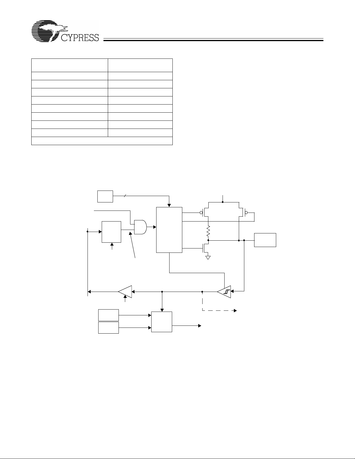
12.0 General Purpose I/O Ports
Ports 0 and 1 provide up to 16 versati le GPIO pins that can be
read or written (the number of pins dep ends on package typ e).
Figure 12-1 shows a diagram of a GPIO port pin.
CY7C63722
CY7C63723
CY7C63743
2
(Data Reg must be 1
for SPI outputs)
Port Read
Interrupt
Logic
SPI Bypass (P0.5–P0.7 only)
(=1 if SPI inactive, or for non-SPI pins)
Internal
Data Bus
GPIO
Mode
Data
Out
Register
Port Write
Interrupt
Polarity
Interrupt
Enable
Figure 12-1. Block Diagram of GPIO Port (one pin shown)
Port 0 is an 8-bit port; Port 1 con t ai ns eith er 2 b it s , P1. 1–P1.0
in the CY7C63723, or all 8 bits , P1.7–P1.0 i n the C Y7C6 3743
parts. Each bit c an a ls o be sel ec ted as an i nterr upt s ou rce for
the microcontroller, as explained in Section 21.0.
The data for each GPIO pin is accessible through the Port
Data registe r. Writes to the P ort Data r egiste r store outgoing
data state for the port pins, while reads from the Port Data
register return the actual logic value on the port pins, not the
Port Data register contents.
V
CC
Q1
Control
14 kΩ
Q3
GPIO
Pin
Q2
Threshold Select
To Capture Timers (P0.0, P0.1)
and SPI (P0.4–P0.7))
To Interrupt
Controller
Each GPIO pin is configured inde pendently. The driving state
of each GPIO pin is determin ed by the value written to th e pin’s
Data Registe r and by two assoc iat ed pin’s Mode0 and M ode1
bits.
The Port 0 Data Register is sh own in Figure 12-2, and the Port
1 Data Register is shown in Figure12-3. The Mode0 and
Mode1 bits for the two GPIO ports are given in Figure 12-4
through Figure 12-7.
Document #: 38-08022 Rev. *B Page 14 of 49
FOR
FOR
CY7C63722
CY7C63723
CY7C63743
Bit # 76543210
Bit Name P0
Read/Write R/WR/WR/WR/WR/WR/WR/WR/W
Reset 00000000
Figure 12-2. Port 0 Data (Address 0x00)
Bit [7:0]: P0[7:0]
1 = Port Pin is logic HIGH
0 = Port Pin is logic LOW
Bit # 76543210
Bit Name P1
Notes Pins 7:2 only in CY7C63743 Pins 1:0 in
all parts
Read/Write R/W R/W R/W R/W R/W R/W R/W R/W
Reset 00000000
Figure 12-3. Port 1 Data (Address 0x01)
Bit [7:0]: P1[7:0]
1 = Port Pin is logic HIGH
0 = Port Pin is logic LOW
Bit # 76543210
Bit Name P0[7:0] Mode0
Read/Write WWWWWWWW
Reset 00000000
Figure 12-4. GPIO Port 0 Mode0 Register (Address 0x0A)
Bit [7:0]: P0[7:0] Mode 0
1 = Port 0 Mode 0 is logic HIGH
0 = Port 0 Mode 0 is logic LOW
Bit # 76543210
Bit Name P0[7:0] Mode1
Read/Write WWWWWWWW
Reset 00000000
Figure 12-5. GPIO Port 0 Mode1 Register (Address 0x0B)
Bit [7:0]: P0[7:0] Mode 1
1 = Port Pin Mo de 1 is logic HIGH
0 = Port Pin Mode 1 is logic LOW
Bit # 76543210
Bit Name P1[7:0] Mode0
Read/Write WWWWWWWW
Reset 00000000
Figure 12-6. GPIO Port 1 Mode0 Register (Address 0x0C)
Bit [7:0]: P1[7:0] Mode 0
1 = Port Pin Mode 0 is logic HIGH
0 = Port Pin Mode 0 is logic LOW
Bit # 76543210
Bit Name P1[7:0] Mode1
Read/Write WWWWWWWW
Reset 00000000
Figure 12-7. GPIO Port 1 Mode1 Register (Address 0x0D)
Bit [7:0]: P1[7:0] Mode 1
1 = Port Pin Mode 1 is logic HIGH
0 = Port Pin Mode 1 is logic LOW
Each pin can be independe ntly configure d as high-impedanc e
inputs, inputs with internal pull-ups, open drain outputs, or
traditional CMOS outputs with selectable drive strengths.
The driving state of ea ch GPIO pin is determi ned by the valu e
written to the pin ’s Da ta Regis ter and by its associat ed Mode0
and Mode1 bits. Table 12-1 lists the configuration states
based on these bits. The GPIO ports default on reset to all
Data and Mode Registers cleared, so the pins are all in a
high-impedance state. The available GPIO output drive
strength are:
• Hi-Z Mode (Mode1 = 0 and Mode0 = 0)
Q1, Q2, and Q3 (Figure 12-1) are OFF . The GPIO pin is not
driven internally . Perfo rming a read from the Port Data Register return the actual logic value on the port pins.
• Low Sink Mode (Mode1 = 1, Mode0 = 0, and the pin ’s Data
Register = 0)
Q1 and Q3 are OFF. Q2 is ON. The GPIO pin is capable of
sinking 2 mA of current.
• Medium Sink Mode (Mode1 = 0, Mode0 = 1, and the pin’s
Data Register = 0)
Q1 and Q3 are OFF. Q2 is ON. The GPIO pin is capable of
sinking 8 mA of current.
• High Sink Mode (Mode1 = 1, Mode 0 = 1, and the pin’s Dat a
Register = 0)
Q1 and Q3 are OFF. Q2 is ON. The GPIO pin is capable of
sinking 50 mA of current.
• High Drive Mode (Mode1 = 0 or 1, Mode0 = 1, and the pin’s
Data Register = 1)
Q1 and Q2 are OFF. Q3 is ON. The GPIO pin is capable of
sourcing 2 mA of current.
• Resistive Mode (Mode 1 = 1, Mode0 = 0, and the pin ’s Data
Register = 1)
Q2 and Q3 are OFF. Q1 is ON. The GPIO pin is pulled up
with an internal 14-kΩ resistor.
Note that open drain mode can be achieved by fixing the Data
and Mode1 Registe rs LOW , an d switching t he Mode0 regi ster .
Input thresholds are CMOS, or TTL as sh own in the t able (See
Section 25.0 for the input threshold voltage in TTL or CMOS
modes). Both input modes include hysteresis to minimize
noise sensitivity. In suspend mode, if a pin is used for a
wake-up interrupt using an external R-C circuit, CMOS mode
is preferred for lowest power.
Document #: 38-08022 Rev. *B Page 15 of 49
 Loading...