

Page 1

PRELIMINARY
,
CY7C63612/13
CY7C63612/13
Low-Speed, Low I/O
1.5 Mbps USB Controller
Cypress Semiconductor Corporation
• 3901 North First Street • San Jose • CA 95134 • 408-943-2600
March 26
1999
Page 2

FOR
FOR
PRELIMINARY
CY7C63612/13
TABLE OF CONTENTS
1.0 FEATURES .....................................................................................................................................5
2.0 FUNCTIONAL OVERVIEW .............................................................................................................6
3.0 PIN ASSIGNMENTS .......................................................................................................................8
4.0 PROGRAMMING MODEL ...............................................................................................................8
4.1 14-bit Program Counter (PC) ...........................................................................................................8
4.2 8-bit Accumulator (A) .......................................................................................................................8
4.3 8-bit Index Register (X) ....................................................................................................................8
4.4 8-bit Program Stack Pointer (PSP) ..................................................................................................8
4.5 8-bit Data Stack Pointer (DSP) ........................................................................................................9
4.6 Address Modes ................................................................................................................................9
4.6.1 Data ........................................................................................................................................................9
4.6.2 Direct ......................................................................................................................................................9
4.6.3 Indexed ................................................................................................................................................... 9
5.0 INSTRUCTION SET SUMMARY ...................................................................................................10
6.0 MEMORY ORGANIZATION ..........................................................................................................11
6.1 Program Memory Organization ......................................................................................................11
6.2 Data Memory Organization ............................................................................................................12
6.3 I/O Register Summary ................................................................................................................... 1 3
7.0 CLOCKING ....................................................................................................................................1 4
8.0 RESET ...........................................................................................................................................1 4
8.1 Power-On Reset (POR) .................................................................................................................14
8.2 Watch Dog Reset (WDR) ............................................................................................................... 1 5
9.0 GENERAL PURPOSE I/O PORTS ...............................................................................................15
9.1 GPIO Interrupt Enable Ports ..........................................................................................................16
9.2 GPIO Configuration Port ................................................................................................................17
10.0 USB SERIAL INTERFACE ENGINE (SIE) .................................................................................1 7
10.1 USB Enumeration ........................................................................................................................1 8
10.2 PS/2 Operation .............. ............... ......................... ............... ............... .............. ...................... ....18
10.3 USB Port Status and Control .......................................................................................................18
11.0 USB DEVICE ...............................................................................................................................1 9
11.1 USB Ports .................................................................................................................................... 1 9
11.2 Device Endpoints (3) ...................................................................................................................19
12.0 12-BIT FREE-RUNNING TIMER .................................................................................................20
12.1 Timer (LSB) .................................................................................................................................2 0
12.2 Timer (MSB) ................................................................................................................................ 2 0
13.0 PROCESSOR STATUS AND CONTROL REGISTER ......................................... ............... .......21
14.0 INTERRUPTS ..............................................................................................................................2 1
14.1 Interrupt Vectors ..........................................................................................................................22
14.2 Interrupt Latency ..........................................................................................................................22
14.2.1 USB Bus Reset Interrupt ....................................................................................................................22
14.2.2 Timer Interrupt ....................................................................................................................................23
2
Page 3

FOR
FOR
PRELIMINARY
TABLE OF CONTENTS
(continued)
CY7C63612/13
14.2.3 USB Endpoint Interrupts .....................................................................................................................23
14.2.4 DAC Interrupt ......................................................................................................................................23
14.2.5 GPIO Interrupt ....................................................................................................................................23
15.0 TRUTH TABLES .........................................................................................................................23
16.0 ABSOLUTE MAXIMUM RATINGS .............................................................................................2 6
17.0 DC CHARACTERISTICS ............................................................................................................27
18.0 SWITCHING CHARACTERISTICS .............................................................................................28
19.0 ORDERING INFORMATION .......................................................................................................30
20.0 PACKAGE DIAGRAM .................................................................................................................30
3
Page 4

FOR
FOR
PRELIMINARY
CY7C63612/13
LIST OF FIGURES
Figure 6-1. Program Memory Space with Interrupt Vector Table .........................................................11
Figure 7-1. Clock Oscillator On-chip Circuit ..........................................................................................14
Figure 8-1. Watch Dog Reset (WDR) ...................................................................................................15
Figure 9-1. Block Diagram of a GPIO Line ...........................................................................................15
Figure 9-2. Port 0 Data 0x00h (read/write) ...........................................................................................16
Figure 9-3. Port 1 Data 0x01h (read/write) ...........................................................................................16
Figure 9-4. Port 2 Data 0x02h (read/write) ...........................................................................................16
Figure 9-5. Port 3 Data 0x03h (read/write) ...........................................................................................16
Figure 9-6. DAC Port Data 0x30h (read/write) ......................................................................................16
Figure 9-7. Port 0 Interrupt Enable 0x04h (write only) ..........................................................................16
Figure 9-8. Port 1 Interrupt Enable 0x05h (write only) ..........................................................................16
Figure 9-9. Port 2 Interrupt Enable 0x06h (write only) ..........................................................................16
Figure 9-10. Port 3 Interrupt Enable 0x07h (write only) ........................................................................ 16
Figure 9-11. GPIO Configuration Register 0x08h (write only) ..............................................................17
Figure 10-1. USB Status and Control Register 0x1Fh ..........................................................................18
Figure 11-1. USB Device Address Register 0x10h (read/write) ...........................................................19
Figure 11-2. USB Device EPA0 Mode Register 0x12h (read/write) .....................................................19
Figure 11-3. USB Device Endpoint Mode Registers 0x14h, 0x16h (read/write) ...................................19
Figure 11-4. USB Device Counter Registers 0x11h, 0x13h, 0x15h (read/write) ..................................20
Figure 12-1. Timer Register 0x24h (read only) ..................................................................................... 20
Figure 12-2. Timer Register 0x25h (read only) ..................................................................................... 20
Figure 12-3. Timer Block Diagram ........................................................................................................20
Figure 13-1. Processor Status and Control Register 0xFFh .................................................................21
Figure 14-1. Global Interrupt Enable Register 0x20h (read/write) ........................................................21
Figure 14-2. USB End Point Interrupt Enable Register 0x21h (read/write) ..........................................22
Figure 18-1. Clock Timing .....................................................................................................................28
Figure 18-2. USB Data Signal Timing ...................................................................................................29
Figure 18-3. Receiver Jitter Tolerance .... ............... ............... .............. ............... ............... ...................29
Figure 18-4. Differential to EOP Transition Skew and EOP Width .......................................................29
Figure 18-5. Differential Data Jitter .......................................................................................................30
LIST OF TABLES
Table 6-1. I/O Register Summary ........................................................................................................13
Table 14-1. Interrupt Vector Assignments ...........................................................................................22
Table 15-1. USB Register Mode Encoding ..........................................................................................23
Table 15-2. Decode tab le f or
Table 15-3
: “Details of M odes for Differing Traffic Conditions” .. ............24
Table 15-3. Details of Modes for Differing Traffic Conditions ..............................................................25
4
Page 5

FOR
FOR
PRELIMINARY
CY7C63612/13
1.0 Features
• Low-cost solution for low-speed applications with low I/O requirements such as mice, gamepads, a nd joystick applications
• USB Specification Compliance
—Conforms to USB Specificat ion, Version 1.1
—Conforms to USB HID Specification, Version 1.1
—Supports 1 device address and 3 data endpoints
—Integrated USB transceiver
• 8-bit RISC microcontroller
—Harvard architecture
—6-MHz external ceramic resonator
—12-MHz internal CPU clock
• Internal memory
—256 bytes of RAM
—6 Kbytes of EPROM (CY7C63612)
—8 Kbytes of EPROM (CY7C63613)
• Interface can aut o-configure to operate as PS2 or USB
• I/O port
—12 General-Purpose I/O (GPIO) pins (Port 0 to 2) capable of sinking 7 mA per pin (t ypical)
—Four GPIO pins (Port 3) capable of sinking 12 mA per pin (typical) wh ich can drive LEDs
—Higher current drive is available by connecting multi ple GPIO pins together to drive an commo n output
—Eac h GPIO port can be configured as input s with internal pull- ups or open drain outputs or tradi tional CMOS outputs
—M askable interrupt s on all I/O pi ns
• 12-bit free-running timer with one microsecond clock ticks
• Watch D o g T i m e r (WDT )
• Internal Power-On Reset (POR)
• Improved output drivers to reduce EMI
• Operating voltage from 4.0V to 5.5V DC
• Operating temperature from 0 to 70 degrees Celsius
• CY7C63612/13 available in 24-pin SOIC packages for production
• Industry-sta ndard programmer support
5
Page 6

FOR
FOR
PRELIMINARY
CY7C63612/13
2.0 Functional Overview
The CY7C63612/13 are 8-bit RISC One Time Programmable (OTP) microcontrollers. The instruction set has been optimized
specifica ll y for USB operation s, although the microcontrollers can be used for a variety of non-USB embedded applications .
The CY7C63612/13 features 16 General-Purpose I/O (GPIO) pins to support USB and other applications. The I/O pins are
grouped int o three ports (P ort 0, 1, and 3) wher e each port can be conf igure d as input s wit h internal pul l-up s, open dr ain out puts,
or tradi ti onal CMOS outputs . 12 GPIO pins (Ports 0 and 1) are rated at 7 mA typical sink current. There are 4 GPIO pins (Port 3)
which are rat ed at 12 mA typical sink current , which allows these pins to drive LEDs . Multiple GPIO pins ca n be connected toget her
to drive a single outp ut f or more driv e current capac ity. Addi tion ally, each I/O pin can be used to generate a GPIO interrupt to the
microcontroller. Note the GPIO interrupts all share the same “GPIO” interrupt vector.
The Cypress microc ontroll ers use an ex ternal 6-MHz cer amic resonato r to provide a re ferenc e to an internal clo ck generat or . This
clock generator reduces the clock-related noise emissions (EMI). The clock generator provides the 6- and 12-MHz clocks that
remain internal to the microcontroller.
The CY7C63612/13 are of fered with two EPROM options t o maximize f lexib ility and mini mize cost . The CY7C63612 has 6 Kb ytes
of EPROM. The CY7C63613 has 8 Kbytes of EPROM.
These parts include power-on reset logi c, a watch dog timer, a vect ored interrupt control ler, and a 12-bi t free-running timer. The
Po wer-On Reset (PO R) lo gic det ects when p ow er is app lied to th e de vi ce , res ets t he logi c to a k nown stat e, an d be gins e xecuting
instructions at EPROM address 0x0000h. The watch dog timer can be used to ensure the firmware never gets stalled for more
than approximately 8 ms. The firmware can get stalled for a variety of r easons, including errors in the code or a hardware failur e
such as waiting for an interrupt that never occurs. The firmware should clear the watchdog timer periodically. If the watch dog
timer is not cleared for approximately 8 ms, the microcontroller wil l generate a hardware wa tch dog reset.
The microcontr oller s upports eight maskab le inter rupts in th e vector ed interrupt c ontroll er. Interrupt sour ces incl ude the USB BusReset, the 128-µs and 1.024-ms outputs from the free-running timer, three USB endpoints, the DAC port, and the GPIO ports.
The timer bits cause an interrupt (if enabled) when the bit toggles from LOW “0” to HIGH “1”. The USB endpoints interrupt after
either the USB host or the USB controller sends a packet to the USB. The DAC ports have an additional level of masking that
allows the user to select which DAC inputs can cause a DAC interrupt. The GPIO ports also have a level of masking to select
which GPIO inputs can cause a GPIO interrupt. For additional flexibility, the input transition polarity that causes an interrupt is
programmable for each pin of the DAC port. Input transition polarity can be programmed for each GPIO port as part of the port
configuration. The interrupt polarity can be either rising edge (“0” to “1”) or falling edge (“1” to “0”).
The free-runn ing 12-bit tim er clocked at 1 MHz pro vides two int errupt sources as noted above (128-µs and 1.024-ms). The timer
can be used to measur e the dur ation of an ev ent under firmware control by read ing the timer twice: once at the start of the event ,
and once after the event is complete. The differ ence between the two readings indicates the duration of the event measured in
microseconds. The upper four bits of the timer are latched into an internal register when the firmware reads the lower eight bits.
A read from t he u pper four bits actually reads dat a from t he internal r egist er , inst ead o f the timer. This feature elimi nat es the n eed
for fi rmware to attempt to compensate if the upper four bits happened to increment right aft er t he lower 8 bits are read.
The CY7C63612/13 include an integrated USB serial interface engine (SIE) that supports the integrated peripherals. The hardware supports one USB device address with three endpoints. The SIE allows the USB host to communicate with the function
integrated into the microcontroller.
Finally, the CY7C63612/13 support PS/2 operation . With appr opriate fi rmware the D+ and D– USB pins can al so be used as PS/
2 clock and data signals. Products u tilizing these devices can be used for USB and/or PS/2 operation with appropriate firmware.
6
Page 7
FOR
FOR
.
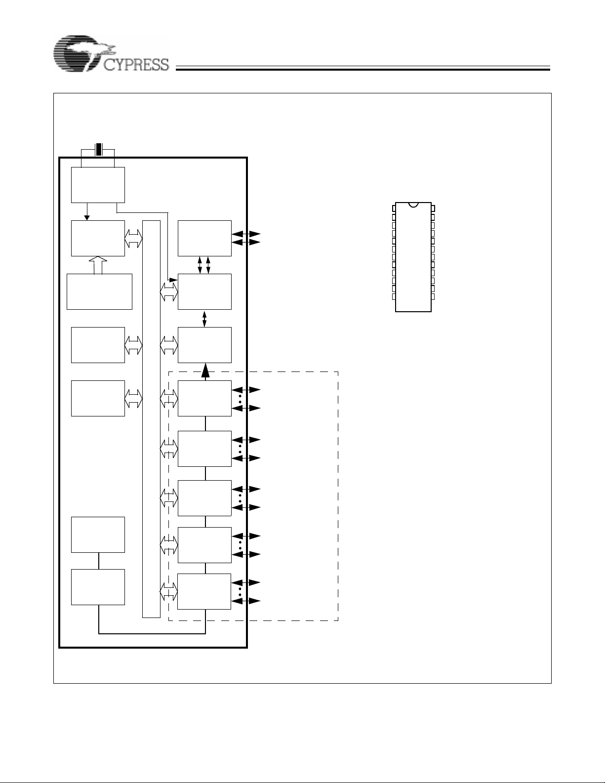
Logic Block Diagram
6-MHz ceramic resonator
OSC
12 MHz
4/6/8 Kbyte
6 MHz
12-MHz
8-bit
CPU
EPROM
RAM
256 byte
8-bit Bus
PRELIMINARY
USB
Transceiver
USB
SIE
Interrupt
Controller
D+
D–
USB
PS/2
PORT
Pin Configuration
CY7C63612/13
24-pin SO IC
1
24 V
2
23
3
22
4
21
5
20
6
19
7
18
17
9
16
10815
11
14
12
13
TOP VIEW
CC
V
SS
P3[6]
P3[4]
P1[2]
P1[0]
P0[6]
P0[4]
P0[2]
P0[0]
XTAL
XTAL
P3[7]
P3[5]
P1[3]
P1[1]
P0[7]
P0[5]
P0[3]
P0[1]
V
Vss
D+
D–
PP
CY7C63612/13
OUT
IN
12-bit
Timer
Watch Do g
Timer
Power-o n
Reset
GPIO
PORT 0
GPIO
PORT 1
GPIO
PORT 2
GPIO
PORT 3
DAC
PORT
P0[0]
P0[7]
P1[0]
P1[7]
P2[0]
P2[7]
P3[0]
P3[7]
DAC[0]
DAC[7]
See Note 1
High Current
Outputs
Note:
1. CY7C63612/13 is not bonded out for all GPIO pins shown in Logic Block Diagram. Refer to pin configuration diagram for bonded out pins. See note on page 16
for firmware code needed for unused GPIO pins.
7
Page 8

FOR
FOR
PRELIMINARY
CY7C63612/13
3.0 Pin Assignments
CY7C63613
Name I/O
D+, D– I/O 1,2 USB differential data; PS/2 clock and data signals
P0[7:0]
I/O
P1[3:0]
7,18,8,17,
9,16,10,15
5,20,6,19 GPIO Port 1 capab le of sinking 7 mA (typical). P1[ 7:4] not bonded out on
I/O
P2
n/a GPIO Port 2 not bonded out on CY7C63612/13. See note on page 16 for firm-
I/O
P3[7:4]
3,22,4,21 GPIO Port 3 capab le of sinking 12 mA (typical). P3[ 3:0] not bonded out on
I/O
DAC I/O n/a DAC I /O Port not bonded out on CY7C63612/13. See not e on page 16 for firm-
XTAL
XTAL
V
PP
V
CC
IN 13 6-MHz ceramic resonator or external clock input
IN
OUT 14 6-MHz ceramic resonator
OUT
11 Pr ogramming voltage supply, ground for normal operation
24 Voltage supply
Vss 12,23 Ground
Description24-Pin
GPIO port 0 capable of sinking 7 mA (typical)
CY7C63612/13. See not e on page 16 for f irmware code nee ded for unused pins .
ware code needed for unused pins.
CY7C63612/13. See not e on page 16 for f irmware code nee ded for unused pins .
ware code needed for unused pins.
4.0 Programming Model
4.1 14-bit Program Counter (PC)
The 14-bit Pr ogra m Counte r (PC) a llo ws acc ess f or up to 8 k ilob ytes of EPR OM usi ng the CY7 C636xx archi tectur e . The pr ogram
counter is cleare d during r ese t, suc h that the fi rst instruc tion ex ec uted af te r a res et is at addr ess 0 x0000h. T his i s typi call y a jump
instruction to a res et handler that initializes the application.
The lower eight bits of the program counter are incremented as instructions are loaded and executed. The upper six bits of the
program counter are inc remented by executing an XPAGE instruction. As a result , the last i nstruction executed within a 256-b yte
“page” of sequential code should be an XPAGE instruction. The assembler directive “XPAGEON ” will cause the assembler to
insert XPAGE instructions automatically. As instructions can be either one or two bytes long, the assembler may occasionally
need to insert a NOP follow ed by an XPAGE for correct execution.
The program counte r of t he ne xt i nstruct ion t o be executed, carry flag, and zer o fla g are sa v ed a s two b ytes on the p rogr am st ack
during an interrupt acknowledge or a CALL instruction. The program counter, carry flag, and zero flag are restored from the
program stack only during a RETI instruction.
Please note the program counter cannot be accessed directly by the firmware. The program stack can be examined by reading
SRAM from location 0x00 and up.
4.2 8-bit Accumulator (A)
The accumulator is the general purpose, do everything register in the architecture where results are usually calculated.
4.3 8-bit Index Register (X)
The index regi ster “X” is av ailab le to the firmware as an auxi liary accumul ator . The X register also allows the processo r to perform
indexed operations by loading an inde x value into X.
4.4 8-bit Program Stac k Pointer ( PSP)
During a rese t, the Progr am Stack P ointer (PSP) is set to z ero. This means the program “stack ” starts at RAM address 0x00 and
“grows” upw ard from there . Note the progr am stac k pointe r is directl y address able unde r firmware control , using the MO V PSP,A
instruction. The PSP supports interrupt service under hardware control and CALL, RET, and RETI instructions under firmware
control.
During an interrupt ac knowledge, interrupts are disabled and the 14-bit program counter, carry flag, and zero flag are written as
two bytes of data memory. The first byte is stored in the memory addressed by the program stack pointer, then the PSP is
8
Page 9

FOR
FOR
PRELIMINARY
CY7C63612/13
incremented. The second byte is stored in memory addressed by the program stack pointer and the PSP is incremented again.
The net effect is to store the pro gram counter and flags on the program “stack” and increment the program stack pointer by tw o.
The Return From I nterrupt (RETI) instruct ion dec rements t he pro gram st ac k point er , then res tores t he second b yt e from memory
addressed by the PSP. The program stack pointer is decremented again and the first byte is restored from memory addressed
by the PSP. After the pr og ram cou nte r and flags ha v e be en r estor ed from st ac k, the inte rrupts are en ab led. The eff e ct i s to res tore
the program counter and flags from the program stack, decrement the program stack pointer b y two, and re-enable interrupts.
The Call Subrout ine (CALL) instruct ion stores the progr am counter and flags on t he program stac k and incremen ts the PSP by two .
The Return From Subroutine (RET) instruction restores the program counter, but not the flags, from program stack and decre-
ments the PSP by two .
4.5 8-bit Data Stack Pointer (DSP)
The Data Stack Pointer (DSP) supports PUSH and POP instructions that use the data stack for temporary storage. A PUSH
instruction wi ll pr e-decr ement the DSP, then write data t o the memory l ocatio n address ed b y the DSP. A POP instruction will read
data from the memory location addressed by the DSP, then post-increment the DSP.
During a reset, the Data Stack Pointer will be set to zero. A PUSH instruction when DSP equal zero will w r ite d a ta a t t h e to p of
the data RAM (address 0xFF). This would write data to the memory area reserved for a FIFO for USB endpoint 0. In non-USB
applications, this works fi ne and is not a problem. For USB applicati ons, it is strongly recommen ded that the DSP is loaded after
reset just below the USB DMA buffers .
4.6 Address Modes
The CY7C63612/13 microcontrollers support three addressing modes for instructions that require data operands: data, direct,
and indexed.
4.6.1 Data
The “Data” add res s mode refers to a data operand tha t is a ctual ly a con st ant encod ed i n the i nstruct ion. As an exa mple , cons ide r
the instruction that loads A with the constant 0xE8h:
• MOV A,0E8h
This instruction will require two bytes of code where the first byte identifies the “MOV A” instruction with a data operand as the
second byte. The second byte of the instruction will be the constant “0xE8h”. A constant may be referred to by name if a prior
“EQU” statement assigns the constant value to the name. For example, the following code is equivalent to the example shown
above:
• DSPINIT: EQU 0E8h
• MOV A,DSPINIT
4.6.2 Direct
“Direct” address mode is used when the data operand is a variable stored in SRAM. In that case, the one byte address of the
variable is encoded in the instruction. As an example, consider an instruction that loads A with the contents of memory address
location 0x10h:
• MOV A, [10h]
In normal usage, variable names are assigned to variable addresses using “EQU” statements to improve the readability of the
assembl er source code. As an example, the fol lowing code is equivalent to the exampl e shown above:
• buttons: EQU 10h
• MOV A,[buttons]
4.6.3 Indexed
“Indexed” address mode allows the firmware to manipulate arrays of data stored in SRAM. The address of the data operand is
the sum of a constant encoded in the instruction and the contents of the “X” register. In normal usage, the constant will be the
“base” address of an array of data and the X register will contain an index that indicates which element of the array is actually
addressed:
• array: EQU 10h
•MOV X,3
• MOV A,[x+array]
This would have the effect of loading A with the fourth element of the SRAM “array” that begins at address 0x10h. The four th
element would be at add ress 0x13h.
9
Page 10

FOR
FOR
PRELIMINARY
CY7C63612/13
5.0 Instruction Set Summary
MNEMONIC operand opcode cycles MNEMONIC operand opcode cycles
HALT 00 7 NOP 20 4
ADD A , ex pr data 01 4 INC A acc 21 4
ADD A,[expr] direct 02 6 INC X x 22 4
ADD A,[X+expr] index 03 7 INC [expr] direct 23 7
ADC A , ex pr data 04 4 INC [X+expr] index 24 8
ADC A,[expr] direct 05 6 DEC A acc 25 4
ADC A,[X+expr] index 06 7 DEC X x 26 4
SUB A,expr data 07 4 DEC [expr] direct 27 7
SUB A,[expr] direct 08 6 DEC [X+expr] index 28 8
SUB A,[X+expr] index 09 7 IORD expr address 29 5
SBB A,expr data 0A 4 IOWR expr address 2A 5
SBB A,[expr] direct 0B 6 POP A 2B 4
SBB A,[X+expr] index 0C 7 PO P X 2C 4
OR A,expr data 0D 4 PUSH A 2D 5
OR A,[expr] direct 0E 6 PUSH X 2E 5
OR A,[X+expr] index 0F 7 SWAP A,X 2F 5
AND A , ex pr data 10 4 SWAP A,DSP 30 5
AND A,[expr] direct 11 6 MOV [ expr],A direct 31 5
AND A,[X+expr] index 12 7 MOV [X+expr],A index 32 6
XOR A,expr data 13 4 OR [expr],A direct 33 7
XOR A,[expr] direct 14 6 OR [X+expr],A index 34 8
XOR A,[X+expr] index 15 7 AND [expr],A direct 35 7
CMP A,expr data 16 5 AND [X+expr],A index 36 8
CMP A,[expr] direct 17 7 XOR [expr],A direct 37 7
CMP A,[X+expr] index 18 8 XOR [X+exp r],A index 38 8
MOV A,expr data 19 4 IOWX [X+expr] index 39 6
MOV A,[ex pr] direct 1A 5 CPL 3A 4
MOV A,[X+expr] index 1B 6 ASL 3B 4
MOV X,expr data 1C 4 ASR 3C 4
MOV X,[ex pr] direct 1D 5 RLC 3D 4
reserved
XPAGE 1F 4 RET 3F 8
MOV A,X 40 4 DI 70 4
MOV X,A 41 4 EI 72 4
MOV PSP,A 60 4 RETI 73 8
CALL addr 50-5F 10
JMP addr 80-8F 5 JC addr C0-CF 5
CALL addr 90-9F 10 JNC addr D0-DF 5
JZ addr A0-AF 5 JACC addr E0-EF 7
JNZ addr B0-BF 5 INDEX addr F0-FF 14
1E RRC 3E 4
10
Page 11

FOR
FOR
PRELIMINARY
6.0 Memory Organization
6.1 Program Memory Organization
after re set Address
14-bit PC 0x0000 Program e xecution begins here after a reset
CY7C63612/13
0x0002 USB Bus Reset interrupt vect or
0x0004 128-µs timer interrupt vector
0x0006 1.024-ms timer interrup t vector
0x0008 USB address A endpoint 0 interrupt vector
0x000A USB address A endpoint 1 interrupt vector
0x000C USB address A endpoint 2 interrupt vector
0x000E Reserved
0x0010 Reserved
0x0012 Reserved
0x0014 DAC interrupt vector
0x0016 GPIO interrupt vector
0x0018 Reserved
0x001A
Program Memory begins here
0x0FFF
0x17FF
6-KB PROM ends here (CY7C63612)
(8K - 32 bytes)
0x1FDF 8-KB PROM ends here (CY7C63613)
Figure 6-1. Program Memory Space with Interrup t Vector Table
11
Page 12

FOR
FOR
PRELIMINARY
CY7C63612/13
6.2 Data Memory Organization
The CY7C63612/13 microcontrollers provide 256 bytes of data RAM. In normal usage, the SRAM is partitioned into four areas:
program stack, data stack , user variables and USB endpoint FIFOs as shown below:
after re set Address
8-bit PSP 0x00
8-bit DSP user
0xE8
0xF0
Program Stac k begins here and grows upward
Data Stack begins her e and grows downward
The user determines the amount of memory required
User V ariables
USB FIFO for Address A endpoint 2
USB FIFO for Address A endpoint 1
0xF8
Top of RAM Memory 0xFF
USB FIFO for Address A endpoint 0
12
Page 13

FOR
FOR
PRELIMINARY
CY7C63612/13
6.3 I/O Register Summary
I/O regist ers are accessed via the I/O Read (IORD) and I/O Wri te (IOWR, IOWX) instruct ions. IORD reads t he selected port into
the accumulator. IOWR writes data from the accumula tor to the selected port. Indexed I/O Write (IOWX) adds the contents of X
to the address in the instruction to form the port address and writes data from the accumulator to the specified port. Note that
specifyin g address 0 (e.g., IO W X 0h) means the I/O port is selected solely by th e contents of X.
T able 6-1. I/O Register Summary
Register Name I/O Address Read/Write Function
Port 0 Data 0x00 R/W GPIO Port 0
Port 1 Data 0x01 R/W GPIO Port 1
Port 2 Data 0x02 R/W GPIO Port 2
Port 3 Data 0x03 R/W GPIO Port 3
Port 0 Interrupt Enable 0x04 W Interrupt enable for pins in Port 0
Port 1 Interrupt Enable 0x05 W Interrupt enable for pins in Port 1
Port 2 Interrupt Enable 0x06 W Interrupt enable for pins in Port 2
Port 3 Interrupt Enable 0x07 W Interrupt enable for pins in Port 3
GPIO Configurati on 0x08 R/W GPIO Ports Configurations
USB Device Addre ss A 0x10 R/W USB Device Address A
EP A0 Counter Register 0x11 R/W USB Address A, Endpoint 0 counter register
EP A0 Mode Register 0x12 R/W USB Address A, Endpoint 0 configuration regi ster
EP A1 Counter Register 0x13 R/W USB Address A, Endpoint 1 counter register
EP A1 Mode Register 0x14 R/C USB Address A, Endpoint 1 configuration registe r
EP A2 Counter Register 0x15 R/W USB Address A, Endpoint 2 counter register
EP A2 Mode Register 0x16 R/C USB Address A, Endpoint 2 configuration registe r
USB Status & Control 0x1F R/W USB upstream port traffic status and control register
Global Interrupt Enable 0x20 R/W Global interrupt enable register
Endpoint Interrupt Enable 0x21 R/W USB endpoint interrupt enables
Timer (LSB) 0x24 R Lower eight bits of free-running timer (1 MHz)
Timer (MSB) 0x25 R Upper four bits of free-run ning timer that are latched
when the lower eig ht bi ts are read.
WDR Clear 0x26 W Watch Dog Reset clear
DAC Data 0x30 R/W DAC I/O
DAC Interrupt Enable 0x31 W Interrupt enable for each DAC pin
DAC Interrupt Polarity 0x32 W Interrupt polarity for each DAC pin
DAC Is ink 0x38-0x3F W One four bit si nk current register for each DAC pin
Processor Status & Control 0xFF R/W Microprocessor sta tus and control
Note:
2. DAC I/O Port not bonded out on CY7C63612/13. See note on page 16 for firmware code needed for unused GPIO pins.
[2]
[2]
[2]
[2]
13
Page 14

FOR
FOR
PRELIMINARY
CY7C63612/13
7.0 Clocking
Clock Distribution
clk1x
XTALOUT
(to USB SIE)
clk2x
(to Microcontroller)
Clock
Doubler
30 pF
30 pF
XTALIN
Figure 7-1. Clock Oscillator On-chip Circuit
The XTALIN and XTAL
external oscillator can be connected to these pins to provide a reference frequency for the internal clock distribution and clock
are the clock pins to the microcontroller. The user can connect a low-cost ceramic resonator or an
OUT
doubler.
An external 6 MHz clo ck can be appli ed to the XTAL
pin is not permissible as the internal clock is ef fectively shorted to ground.
pin if the XTAL
IN
pin is left open. Please note that groundi ng the XTAL
OUT
OUT
8.0 Reset
The USB Controll er supports three t ypes of rese ts. All r egisters are restor ed to thei r defau lt states duri ng a reset. The USB Device
Addresses ar e s et t o 0 and al l i nter rupts are di sabl ed. I n addition, the Pr ogram Sta ck P o inter ( PSP) and Dat a Stack P oi nter (D SP)
are set to 0x00. For USB applications, the firmware should set the DSP below 0xE8h to avoid a memory conflict with RAM
dedicated to USB FIFOs . The assembly instruc ti ons to do this are shown below :
Mov A, E8h ; Move 0xE8 hex int o Accumulator
Swap A,dsp ; Swap accumulator value into dsp register
The three reset types are:
1. Power-On Reset (POR)
2. Watch Dog Reset (WDR)
3. USB Bus Reset (non hardware reset)
The occurrence of a reset is recorded in the Pro cessor Status and Cont rol Register located at I/O address 0xFF. Bits 4, 5, and 6
are used to record the occurrence of POR, USB Reset, and WDR respectively. The firmware can interrogate these bits to
determine the cause of a reset.
The microcontroller begins execution from ROM address 0x0000h after a POR or WDR reset. Although this looks like interrupt
vector 0, there is an important difference. Reset processing does NOT push the program counter, carry flag, and zero flag onto
program stack. That means the reset handler in firmware should initialize the hardware and begin executing the “main” loop of
code. Attempting to execute either a RET or RETI in the reset handler will cause unpredictable execution results.
8.1 Power-On Reset (POR)
Po wer -On Reset ( POR) o ccur s e v ery t ime the VCC voltage t o the de vice r amps fr om 0V t o an i nternall y defi ned t rip v oltag e ( Vrst) ,
of approximately 1/2 full supply voltage. In addition to the normal reset initialization noted under “Reset,” bit 4 (PORS) of t he
Processor Status and Control Register is set to “1” to indicate to the firmware that a power on reset occurred. The POR event
forces the GPIO ports int o input mode (high impedance), and the state of Port 3 bit 7 is used to control how the part will respond
after the POR releases.
If Port 3 bit 7 is high (pulled to V
permanent power down/suspend mode, waiting for the USB IO to go to one of Bus Reset, K (resume) or SE0. If Por t 3 bit 7 is
still HIGH when the part comes out of suspend, then a 128-µs timer starts, delaying CPU operation until the ceramic resonator
has stabilized.
If Port 3 bit 7 was LOW (pulled to V
continui ng to run as re set.
Firmware should clear the POR Status (PORS) bit in register FFh before going into suspend as this statu s bit selects the 128-µs
or 128-ms start-up timer value as f ollows: IF P ort 3 bit 7 is HIGH then 128-µs is alwa y s used; ELSE if PORS is HIGH the n 128- ms
is used; EL S E 128-µs is used.
) and the USB IO are at the idle state (DM HIGH and DP LOW) the part will go into a semi-
CC
) the part will start a 128-ms timer, delaying CPU operation until VCC has stabilized, then
SS
14
Page 15

FOR
FOR
PRELIMINARY
CY7C63612/13
8.2 Watch Dog Reset (WDR)
The Watc h Dog Timer Reset (WDR) occur s when the Most Sign ificant Bit (MSB) of the 2-bit W atch Dog Tim er Register tr ansitions
from LOW to HIGH. In addition to the normal reset initialization noted under “Reset,” bit 6 of the Processor Status and Control
Register is set to “1” to indicate to the firmware that a watch dog reset occurred.
8.192 ms
to 14.336 ms
2.048 ms
At least 8.192 ms
since la st w r ite to W D T
The Watch Dog Timer is a 2-bit timer clocked by a 4.096-ms clock (bit 11) from the free-running timer. Writing any value to the
write-only Watch Dog Clear I/O port (0x26h) will clear the Watch Dog Timer.
In some applications, the Watch Dog Timer may be cleared in the 1.024-ms timer interrupt s ervice routine. If the 1.024-ms timer
interrupt service routine does not get executed for 8.192 ms or more, a Watch Dog Timer Reset will occur. A Watch Dog Timer
Reset lasts for 2.048 ms after which the microcontroller begins execution at ROM address 0x0000h. The USB transmitter is
disabled by a Wat ch Dog Reset because the USB Device Address Register is cleared. Otherwise, the USB Controller would
respond to all address 0 transactions. The USB transmitter remains disabled until the MSB of the USB address register is set.
WDR goes high
for 2.048 ms
Execution begins at
Reset Vector 0X00
Figure 8-1. Wat ch Dog Reset (WDR)
9.0 General Purpose I/O Ports
V
CC
Q1
7 k
Ω
Q2
to Interrupt
Controller
Q3
ESD
GPIO
Pin
Internal
Data Bus
GPIO
CFG
Interrupt
Enable
Port Write
Internal
Buffer
Data
Out
Latch
Port Read
mode
2 bits
Control
Control
Figure 9-1. Bloc k Diagram of a GPIO Line
Ports 0 to 2 provide 24 GPIO pins that can be read or written. Each port (8 bits) can be configured as inputs with internal pul lups, open drain outputs, or traditional CMOS outputs. Please note an open drain output is also a high-impedance (no pull-up)
input. All of th e I/O pins within a giv en port have t he same confi gurat io n. P orts 0 to 2 are consi dered l ow curr ent driv e with typical
current sink capability of 7 mA.
The internal pu ll-u p resi sto rs are t ypica lly 7 kΩ. Two factors go v ern the ena b ling a nd disab l ing of the i nternal pu ll- up resi stors : the
port configuration selected in the GPIO Configuration register and the state of the output data bit. If the GPIO Configuration
selected i s “Resistive” and the out put data bit i s “1,” then t he internal pull-up resistor is enabled for that GPIO pin. Otherwise, Q1
is turned off and the 7-kΩ pull-up is disabled. Q2 is “ON” to sink current whenever the output data bit is written as a “0.” Q3
15
Page 16

FOR
FOR
PRELIMINARY
CY7C63612/13
provides “HIGH” source current when the GPIO port is configured for CMOS outputs and the output data bit is written as a “1”.
Q2 and Q3 are sized to sink and source, respectively, roughly the same amount of current to support traditional CMOS outputs
with symmetric drive.
P0[7] P0[ 6] P0[5] P0[4] P0[3] P0[2] P0[1] P0[0]
Figure 9-2. Port 0 Data 0x00h (read/write)
P1[7] P1[6] P1[5] P1[4] P1[3] P1[2] P1[1] P1[0]
Figure 9-3. Port 1 Data 0x01h (read/write)
P2[7] P2[6] P2[5] P2[4] P2[3] P2[2] P2[1] P2[0]
Figure 9-4. Port 2 Data 0x02h (read/write)
P3[7] P3[6] P3[5] P3[4] P3[3] P3[2] P3[1] P3[0]
Figure 9-5. Port 3 Data 0x03h (read/write)
Low current out puts
0.2 mA to 1.0 mA typical
High current outputs
3.2 mA to 16 mA typical
DAC[7] DAC[6] DAC[5] DAC[4] DAC[3] DAC[2] DAC[1] DAC[0]
Figure 9-6. DAC Port Data 0x30h (read/write)
Port 3 has eight GPIO pins. Port 3 (8 bits) can be configured as inputs with internal pull-ups, open drain outputs, or traditional
CMOS outputs. An open drain output is also a high-impedance input. Port 3 offers high current drive with a typical current sink
capability of 12 mA. The internal pull-up resistors are typically 7 kΩ.
Special care should be exercised with any unused GPIO data bits. An unused GPIO data bit, either a pin on the chip or
NOTE:
a port bit that i s not bo nded on a p articular pac kage , must not be left floa ting whe n the device enters the suspen d stat e. I f a GPIO
data bit is left floating, the leakage current caused by the floating bit may violate the suspend current limitation specified by the
USB Specific ation. If a ‘1’ is written to the unused data bit and the port is configured with open drain outputs, the unused data bi t
will be in an indeterminate s tate. Therefore, if an unused port bit is programmed in open-drai n m ode, it must be written with a ‘0. ’
Notice that the CY7C63612/ 13 will always requi re that data bits P1[7:4], P2[7:0], P3[3:0] and DAC[7:0] be written with a ‘0.’
During reset, all of the GPIO pins are set to output “1” (input) with the internal pull-up enabled. In this state, a “1” will always be
read on that GPIO pin unless an external current sink drives the output to a “0” state. Writing a “0” to a GPIO pin enables the
output curren t sink to ground (LOW) and disables the internal pull-up for that pi n.
9.1 GPIO Int errupt Enable Ports
During a reset, GPIO interrupts are disabled by clearing all of the GPIO interrupt enable ports. Writing a “1” to a GPIO Interrupt
Enable bit ena bles GPIO interrupts from the corresponding input pi n.
P0[7] P0[6] P0[5] P0[4] P0[3] P0[2] P0[1] P0[0]
Figure 9-7. Port 0 Interrupt Enable 0x04h (write only)
P1[7] P1[6] P1[5] P1[4] P1[3] P1[2] P1[1] P1[0]
Figure 9-8. Port 1 Interrupt Enable 0x05h (write only)
P2[7] P2[6] P2[5] P2[4] P2[3] P2[2] P2[1] P2[0]
Figure 9-9. Port 2 Interrupt Enable 0x06h (write only)
P3[7] P3[6] P3[5] P3[4] P3[3] P3[2] P3[1] P3[0]
Figure 9-10. Port 3 Interrupt Enable 0x07h (write only)
16
Page 17

FOR
FOR
PRELIMINARY
CY7C63612/13
9.2 GPIO Confi guration Port
Every GPIO port can be programmed as inputs with internal pull-ups, open drain outputs, and traditional CMOS outputs. In addition, the i nterrupt polarity f or each po rt can be progr ammed. With posi tiv e int errupt pol arit y, a rising edge (“0” to “1”) on an input
pin causes an i nterru pt. Wit h ne gativ e pol arity, a falli ng edge ( “ 1” to “ 0”) on an input pin ca uses an inte rrupt. As sh own in the tabl e
below, when a GPIO port is configured with CMOS outputs, interrupts fr om that port are disabled. The GPIO Configuration Port
register provides two bits per port to program these features. The possibl e port configurations are:
Port Configuration bits Pin Interrupt Bit Driver Mode Interrupt Polarit y
11 X Resistive 10 0 CMOS Output disabled
10 1 Open Drai n disabled
01 X Open Drain 00 X Open Drain + (defaul t)
In “Resistive” mode, a 7-kΩ pull-up res istor is conditi onall y enable d for all pins of a GPIO port. The resist or is en abled for any pin
that has been written as a “1.” The resistor is disabled on any pin that has been written as a “0”. An I/O pin will be driven high
through a 7-kΩ pull-up re sistor when a “1” has be en written to the pin. Or the output pin wil l be driven LOW, with t he pull-up disabled, when a “0” has bee n written to the pin. An I/O pin that has been written as a “1” can be used as an input pin with an integrated 7-kΩ pull-up resistor. Resistive mode selects a negative (falling edge) interrupt polarity on all pins that have the GPIO
interrupt enabled.
In “CMOS” mode, all pins of the GPI O port ar e outputs that are activ ely driven. The current so urce and sink capacity are roughly
the same (symmetric out put drive). A CMOS port is not a possibl e source for interrupt s.
A port configured in CMOS mode has interrupt generation disabled, yet the interrupt mask bits serve to control port direction. If
a port’s ass ociat ed Inter rupt Mas k bi ts are cleare d, thos e port b its ar e stri ctl y output s. If the In terru pt Mas k bits are set then th ose
bits will be open drain inputs. As open drain inputs, if the ir data output values are ‘1’ those port pins will be CMOS inputs (HIGH
Z output).
In “Open Drain” mode the internal pull-up resistor and CMOS driver (HIGH) are both disabled. An I/O pin that has been written
as a “1” can be used as either a hi gh-impedance input or a three-state output. An I/O pin that has been written as a “0” will drive
the output LOW. The interrupt polarity for an open drain GPIO port can be selected as either positive (rising edge) or negative
(falling edge).
During reset, all of the bits in the GPIO Configuration Register are written with “0”. This selects the default configuration: Open
Drain output, positive interrupt polarity for all GPIO ports.
7 6 5 4 3 2 1 0
Port 3
Config Bit 1
Port 3
Config Bit 0
Port 2
Config Bit 1
Port 2
Config Bit 0
Port 1
Config Bit 1
Port 1
Config Bit 0
Port 0
Config Bit 1
Port 0
Config Bit 0
Figure 9-11. GPIO Configuration Register 0x08h (wri te only)
10.0 USB Serial Interface Engine (SIE)
The SIE allows t he microcontrolle r to communicate with the USB host. The SIE simplifi es the interfac e between the microco ntroller
and USB by incorporating hardware that handles the following USB bus activity independently of the microcontroller:
• Bit stuffing/unstuffing
• Checksum generation/chec king
•ACK/NAK
• Token type identification
• Address checking
Firmware is required to handle the rest of the USB interface with the following tasks:
• Coordinate enumeration by res ponding to set-up pack ets
• Fill and empty the FIFOs
• Suspend/Resume coordination
• Verify and select Data t oggle values
17
Page 18

FOR
FOR
PRELIMINARY
CY7C63612/13
10.1 USB Enumeration
The enumeration sequence is shown below:
1. The host computer sends a
packet followed by a
Setup
packet to USB address 0 requesting the Device descriptor.
Data
2. The USB Controller decodes the request and retrieves its Device descriptor from the program memory space.
3. The host com puter performs a control read sequ ence and the USB Cont roller r esponds b y s ending the De v ice d escri ptor ov er
the USB bus.
4. After receivi ng the descriptor , the host computer sends a
packe t f ollowed b y a
Setup
packet to address 0 assigning a
Data
new USB address to the device.
5. The USB Controller stor es the new address in its USB Device Address Regi ster after the no-data cont rol sequence is compl ete.
6. The host sends a request for the Device descriptor using the new USB address.
7. The USB Controller decodes the request and retrieves the Device descriptor from the pro gram memory.
8. The host perf orms a contr ol read sequenc e and the USB Cont roller responds by sendi ng its De vice descriptor over t he USB bus .
9. The host generates control reads to the USB Controller to request the Configuration and Report descriptors.
10.The USB Controller retriev es the descriptors from its pr ogram space and returns the data to the host over the USB.
10.2 PS/2 Operation
PS/2 operatio n is possible with the CY7C636xx seri es through the use of firmwar e and several operating modes . The first enablin g
feature:
1. USB Bus reset on D+ and D− is an interrupt that can be disabled;
2. USB traffic can be disabled via bit 7 of the USB register;
3. D+ and D− can be monitored and driven via firmware as independent port bits.
Bits 5 and 4 of the Upstream Status and Control register are directly connected to the D+ and D− USB pins of the CY7C636xx.
These pins const antly monitor the le vels of these signals with CMOS inpu t thresholds . Firmware can poll and decod e these signals
as PS/2 clock and dat a.
Bits [2:0] defaults to ‘ 000’ at reset which allows the USB SI E to control output on D+ and D−. Firmware can o verride the SIE and
directly control the st ate of these pins via these 3 control bits. Since PS/2 is an open drain signaling protocol, thes e modes allow
all 4 PS/2 states to be gener ated on the D+ and D− pins
10.3 USB Port Status and Control
USB status and control is regulated by the USB Status and Control Register located at I/O address 0x1Fh as shown in
. This is a read/writ e regi ster. All reserved bits must be written to zero. All bits i n the register are cleared during reset.
10-1
7 6 5 4 3 2 1 0
R R R/W R/W R/W R/W
Reserved Reserved D+ D– Bus Activity Control
Bit 2
Control
Bit 1
Figure 10-1. USB Status and Control Register 0x1Fh
The Bus Activity bit is a “sticky” bit that indicates if any non-idle USB event has occurred on the USB bus. The user firmware
should check and clear this bit periodically to detect any loss of bus activity. Writing a “0” to the Bus Activity bit clears it while
writing a “1” preserves the current value. In other words, the firmware can clear the Bus Activity bit, but only the SIE can set it.
The 1.024-ms timer interrupt service routine is normally used to check and clear the Bus Activity bit. The following table shows
how the control bits are encoded for this register.
Figure
Control
Bit 0
18
Page 19

FOR
FOR
PRELIMINARY
Control Bits Control actio n
000 Not for cing (SIE cont r o l s driver )
001 Force K (D+ HIGH, D– LOW)
010 Force J (D+ LOW, D– HIGH)
011 Force SE0 (D+ LOW, D– LOW)
100 Force SE0 (D− LOW, D+ LOW)
101 Force D− LOW, D+ HiZ
110 Force D− HiZ, D+ LOW
111 Force D− HiZ, D+ HiZ
CY7C63612/13
11.0 USB Device
USB Device Address A includes three endpoints: EPA0, EPA1, and EPA2. End Poi nt 0 (EPA0) allows t he USB host to recognize,
set up, and control the device. In particular, EPA0 is used to receive and transmit control (including set-up) pack ets.
11.1 USB Ports
The USB Controller provides one USB device address with three endpoints. The USB Device Address Register contents are
cleared during a reset, setting the USB device address to zero and marking this address as disabled.
format of the USB Address Regi ster.
Figure 11-1
shows the
Device
Address
Enable
Bit 7 (Device Address Enable) in the USB Device Address Register must be set by firmware before the serial interface engine
(SIE) will respond to USB traffic to this address. The Device Address in bits [6:0] must be set by firmware during the USB enumeration process to an address assigned by the USB host that does not equal zero. This register is cleared by a hardware reset
or the USB bus reset.
Device
Address
Bit 6
Device
Address
Bit 5
Figure 11-1. USB Device Address Register 0x10h (read /write)
Device
Address
Bit 4
Device
Address
Bit 3
Device
Address
Bit 2
Device
Address
Bit 1
Device
Address
Bit 0
11.2 Device Endpoints (3)
The USB controller communicates with the host using dedicated FIFOs, one per endpoint. Each endpoint FIFO is implemented
as 8 bytes of dedicated SRAM. There are three endpoints defined for Device “A” that are labeled “EPA0,” “EPA1,” and EPA2.”
All USB de vices ar e requi red t o ha ve an endpo int n umber 0 (EPA0) that is used to i niti ali ze and con trol the USB de vice . End P oi nt
0 provides access to the device configuration information and allows generic USB status and control accesses. End Point 0 is
bidirect ional as the USB controller can both receive and tran sm it data.
The endpoint mode registers are cleared during reset. The EPA0 endpoint mode register uses the format shown below:
Endpoint 0
Set-up
Received
Bits[7:5] in the endpoint 0 mode registers (EPA0) are “sticky” status bits that are set by the SIE to report the type of token that
was most recently received. The sticky bits must be cleared by firmware as part of the USB processing.
The endpoint mode registers for EPA1 and EPA2 do not use bits [7:5] as shown below:
Endpoint 0
In
Received
Endpoint 0
Out
Received
Figure 11-2. USB Device EPA0 Mode Register 0x12h (read/write)
Acknowledge Mode
Bit 3
Mode
Bit 2
Mode
Bit 1
Mode
Bit 0
Reserved Reserved Reserved Acknowledge Mode
Bit 3
Figure 11-3. USB Device Endpoint Mode Registers 0x14h, 0x16h (read/write)
The ‘Acknowledge’ bit is set whenever the SIE engages in a transaction that completes with an ‘ACK’ packet.
19
Mode
Bit 2
Mode
Bit 1
Mode
Bit 0
Page 20

FOR
FOR
PRELIMINARY
The ‘set-up’ PID status (bit[7]) is forced HIGH from the start of the data packet phase of the set-up transaction, until the start of
the ACK packet returned by the SIE. The CPU is prevented from clearing this bit during this interval, and subsequently until the
CPU first does an IORD to this endpoi nt 0 mode register .
Bits[6:0] of the endpoint 0 mode register are locked from CPU IOWR operations only if the SIE has updated one of these bits,
which the SIE does only at the end of a pac ket transact ion (set-up ... Data .. . ACK, or Out .. . Data ... ACK, or In ... Data ... ACK).
The CPU can unlock these bits by doing a subsequent I/O read of this register.
Firmware must do an IORD after an IOWR to an endpoint 0 register to verify that the contents have changed and that the SIE
has not updated these values.
While the ‘set-up’ bit is set , the CPU cannot write to the DM A buffers at memory locations 0xE0 t hrough 0xE7 and 0xF8 through
0xFF. This prevents an incoming set-up transaction from conflicting with a previous In data buffer filling operation by firmware.
The mode bits (bits [3:0]) in an Endpoint Mode Register control how the endpoint responds to USB bus traffic. The mode bit
encoding is shown in Section 15.0.
The format of the endp oint Device counter registers is shown below:
Data 0/1
Toggle
Bits 0 to 3 indicate the number of data bytes to be transmitted during an IN packet, valid values are 0 to 8 inclusive. Data Valid
bit 6 i s used f or OUT and set-u p tok ens only. Data 0/1 Toggle bit 7 selects the D AT A packet ’s toggle state: 0 f or DAT A0, 1 f or DA TA1.
Data Valid Reserved Reserved Byte count
Bit 3
Figure 11-4. USB Device Counter Registers 0x11h, 0x13h, 0x15h (read/write)
Byte count
Bit 2
CY7C63612/13
Byte count
Bit 1
Byte count
Bit 0
12.0 12-bit Free-running Timer
The 12-bit timer provides two interrupts (128-µs and 1.024-ms) and allows the firmware to directly time events that are up to 4
ms in duration. The lower 8 bits of the timer can be read directly by the firmware. Reading the lower 8 bits latches the upper 4
bits into a temporary register. When the firmware reads the upper 4 bits of the timer, it is actually reading the count stored in the
temporary register. The effect of this logic is to ensure a stable 12-bit timer value can be read, even when the two reads are
separated in time.
12.1 Timer (LSB)
Timer
Bit 7
Timer
Bit 6
Timer
Bit 5
Figure 12-1. Timer Regis ter 0x24h (read only)
Timer
Bit 4
Timer
Bit 3
Timer
Bit 2
Timer
Bit 1
Timer
Bit 0
12.2 Timer (MSB)
Reserved Reserved Reserved Reserved Timer
Bit 11
Figure 12-2. Timer Regis ter 0x25h (read only)
Timer
Bit 10
Timer
Bit 9
Timer
Bit 8
1.024-ms interrupt
128-
s interrupt
µ
10 9 7856 432
1 011
1-MHz clock
L1 L0L2L3
D3 D2 D1 D0 D7 D6 D5 D4 D3 D2 D1 D0
8
Figure 12-3. Timer Block Diagram
20
To Timer R eg ister
Page 21

FOR
FOR
PRELIMINARY
CY7C63612/13
13.0 Processor Status and Control Register
7 6 5 4 3 2 1 0
R R/W R/W R/W R/W R R/W R/W
IRQ
Pending
The “Run” (bit 0) is manipulated b y the HALT instruction. When Halt is e xecuted, the processor cl ears the run bit and halts at the
end of the current instruction. The processor remains halted until a reset (power on or watchdog). Notice, when writing to the
processor status and control register, the run bit should always be written as a “1”.
The “Single Step” (bit 1) is provided to support a hardware debugger. When single step is set, the processor will execute one
instruction and halt (clear the run bit). Thi s bit m ust be cleared for normal operation.
The “Interru pt Mask” (bit 2) shows whether interrupts are enab led or disable d. The firmware has no direct control over this bit as
writing a zero or one to this bit position will have no effect on interrupts. Instructions DI, EI, and RETI manipulate the internal
hardware that controls the state of the interrupt mask bit in the Processor Status and Control Regist er.
Writing a “1” to “Suspend, Wait for Interrupts” (bit 3) will halt the processor and cause the microcontr oll er to enter the “suspend”
mode that significantly reduces power consumption. A pending interrupt or bus activity will cause the device to come out of
suspend. After coming out of suspend, the devi ce will res ume fi rmware e x ecuti on at the instruct ion followin g the IO WR which pu t
the part into suspend. An IOWR that attempts to put the part into suspend will be ignored if either bus activity or an interrupt is
pending.
The “P ower-on Reset” (bi t 4) is only set to “1” during a power on reset. The firmware can check bits 4 and 6 in the reset handler
to determine whether a reset was caused by a power on condition or a watchdog timeout. PORS is used to determine suspend
start-up timer val ue of 128 µs or 128 ms.
The “USB Bus Reset” ( bit 5) wi ll occ ur when a USB b us r eset i s receiv ed. The USB Bus Reset is a si ngled- ende d zero ( SE0) tha t
lasts more than 8 microseconds. An SE0 is defined as the condition in which both the D+ line and the D– line are LOW at the
same time. When the SIE detects this condition, the USB Bus Reset bit is set in the Processor Status and Control register and
an USB Bus Reset interrupt is generated. Please note this is an interrupt to the microcontroller and does not actually reset th e
processor.
The “Watch Dog Reset” (bit 6) is set during a reset initiated by the watch dog timer. This indicates the watch dog timer went for
more than 8 ms between w atch dog clears.
The “IRQ Pending” (bit 7) indicates one or more of the interrupts has been recognized as active. The interrupt acknowledge
sequence should clear this bit until the ne xt interrupt is detec ted.
During power-on reset, the Processor Status and Control Register is set to 00010001, which indicates a power-on reset (bit 4
set) has occurr ed and no interrupts are pending (bi t 7 cl ear) yet.
During a watch dog reset, the Pr ocessor Status and Control Regist er is set to 01000001, which indicates a watch dog reset (bit
6 set) has occurred and no interrupts are pending (bit 7 clear) yet.
Watc h Dog
Reset
USB Bus
Reset
Figure 13-1. Processor Status and Control Register 0xFFh
Power-on
Reset
Suspend, Wait
for Interrupt
Interrupt
Mask
Single Step Run
14.0 Interrupts
All interrupts are maskable by the Global Interrupt Enable Register and the USB End Point Interrupt Enable Register. Writing a
“1” to a bit posi tion en ab les th e inter rupt asso ciated with th at bit posit ion . During a reset , the c onte nts the Global I nterrupt Enab l e
Register and USB End Point Interrupt Enable Register are cleared, effectively disabling all interrupts.
7 6 5 4 3 2 1 0
R/W R/W R/W R/W R/W
Reserved Reserved GPIO
Interrupt
Enable
Figure 14-1. Global Interrupt Enable Register 0x20h (read/write)
DAC
Interrupt
Enable
Reserved 1.024-ms
21
Interrupt
Enable
128-µsec
Interrupt
Enable
USB Bus RST
Interrupt
Enable
Page 22

FOR
FOR
PRELIMINARY
CY7C63612/13
7 6 5 4 3 2 1 0
R/W R/W R/W
Reserved Reserved Reser ved Reserved Reserved EPA2
Interrupt
Enable
EPA1
Interrupt
Enable
EPA0
Interrupt
Enable
Figure 14-2. USB End Point Interrupt Enable Register 0x21h (read/write)
Pending interrupt requests are recognized during the last clock cycle of the current instruction. When servicing an interrupt, the
hardware will first disable all interrupts by clearing the Interrupt Enable bit in the Processor Status and Control Register. Next,
the interrupt latch of the current interrupt is cleared. This is followed by a CALL instruction to the ROM address associated with
the interrupt being serviced (i.e., the Interrupt Vector). The instruction in the interrupt table is typically a JMP instruction to the
address of the Interrupt Service Ro uti ne (ISR). The user can re-enabl e interrupts in the interrupt service routine by executing an
EI instruction. Interrupts can be nested to a level limited only by the available stack space.
The Program Counter value as well as the Carry and Zero flags (CF, ZF) are automatically stored onto the Program Stack by the
CALL instruction as part of the interrupt acknowledge process. The user firmware is responsible for insuring that the processor
state is preserved and restored during an interrupt. The PUSH A instruction should be used as the first command in the ISR to
sav e the accu mul ator v a lue and t he POP A inst ructio n shou ld be used just be fo re t he RETI i nstruct ion to r estor e the accu mul ator
value. The program counter CF and ZF are restored and interrupts are enabled when the RETI instruction is executed.
14.1 Interrupt Vectors
The Interrupt Vectors supported by th e USB Control ler a re list ed i n
Table 14-1
instruction e xec uted after a reset is at PROM address 0x0000h— which corresp onds to the first entry in the Inter rupt V ector Table.
Because the JMP instruction is 2 bytes long, the interrupt vectors occupy 2 bytes.
. Although Rese t is no t an int errupt , per se , the firs t
T able 14-1. Interrupt Vector Assignments
Interrupt Vector Number ROM Address Function
not applicable 0x0000h Execution after Reset begins here
1 0x0002h USB Bus Reset interrupt
2 0x0004h 128-µs timer interrupt
3 0x0006h 1.024-ms timer interrupt
4 0x0008h USB Address A Endpoint 0 interrupt
5 0x000Ah USB Address A Endpoint 1 interrupt
6 0x000Ch USB Address A Endpoint 2 interrupt
7 0x000Eh Reserved
8 0x0010h Reserved
9 0x0012h Reserved
10 0x0014h DAC interrupt
11 0x0016h GPIO interrupt
12 0x0018h Reserved
14.2 Interrupt Latency
Interrupt latency can be calculated from the followi ng equation:
Interrupt Latency = (Number of clock cycles remaining in the cur rent instruction) + (10 clock cycles for the CAL L instruction) +
For example, if a 5 clock cycle instruction such as JC is being executed when an interrupt occurs, the first instruction of the
Interrupt Service Routine wil l execute a min. of 16 clocks (1+10+5) or a max. of 20 clocks (5+10+5) after the interrupt is issued.
Remember that th e interrupt latches are sam pled at the rising edge of the last clock cycle in the cur rent instruction .
(5 clock cycles for the JMP inst ruction)
14.2.1 USB Bus Reset Interrupt
The USB Bus Reset interrupt is asserted when a USB bus reset condition is detected. A USB bus reset is indicated by a single
ended zero (SE0) on th e upstream port for more than 8 microseconds.
22
Page 23

FOR
FOR
PRELIMINARY
CY7C63612/13
14.2.2 Timer Interrupt
There are two timer interrupts: the 128-µs interrupt and the 1.024-ms interrupt. The user should disable both timer interrupts
before going into t he suspend mode to avo id possible c onflicts bet ween servicing the int errupts first or the suspend request first.
14.2.3 USB Endpoint Interrup ts
There are t hree USB endpo int i nter rupts, on e pe r endpoi nt. The USB endpoi nts i nterru pt aft er t he either t he USB host or th e USB
controller sends a packet to the USB.
14.2.4 DAC Interrupt
Each DAC I/O pin can generate an interrupt, if enabled.The interrupt polarity for each DAC I/O pin is programmable. A positive
polarity is a rising edge input while a negative polarity is a falling edge input. All of the DAC pins share a single interrupt vector,
which means the firmware will need to read the DAC port to determine which pin or pins caused an interrupt.
Please note that if one DAC pin triggered an interrupt, no other DAC pins can cause a DAC interrupt until that pin has returned
to its i nacti ve (n on-trigger ) state or t he corres ponding in terrupt en ab le bi t is c leared . The USB Cont roll er do es n ot ass ign in terrup t
priority to different DAC pins and the DAC Interrupt Enable Register is not cleared during the interrupt acknowledge process.
14.2.5 GPIO Inter r up t
Each of the 32 GPIO pi ns can generate an int errupt, if enabled. The interrupt polarit y can be pr ogrammed for each GPIO port as
part of the GPIO configuration. All of the GPIO pins share a single interrupt vector, which means the firmware will need to read
the GPIO ports with enabled interrupts to determine which pin or pins caused an interrupt.
Please note th at if one port pin t riggered an int errupt, no other port pins can cause a GPIO interrup t until that port pin has ret urned
to its inactive (non-trigger) state or its corresponding port interrupt enable bit is cleared. The USB Controller does not assign
interrupt priority to different port pins and the Port Interrupt Enable Registers are not cleared during the interrupt acknowledge
process.
15.0 Truth Tables
T able 15-1. USB Register Mode Encoding
Mode
Disable
Nak In/Out
Status Out Only
Stall In/Out
Ignore I n /Out
Isochronous Out
Status In Only
Isochronous In
Nak Out
Ack Out
Nak Out - Status
In
Ack Out - Status
In
Nak In
Ack In
Nak In - Status
Out
Ack In - Status
Out
Encoding
0000
0001
0010
0011
0100
0101
0110
0111
1000
1001
1010
1011
1100
1101
1110
1111
Setup In Out Comments
ignore ignore ignore Ignore all USB traffic to this endpoint
accept NAK NAK Forced from Set-up on Control endpoint, from modes other
accept stall check For Control endpoints
accept stall stall For Control endp oints
accept ignore ignore For Control endpoints
ignore ignore always Av ailable to low speed devices, future USB spec
accept TX 0 stall F or Control Endpoints
ignore TX cnt ignore Availab le to low speed devi ces, future USB spec
ignore ignore NAK An ACK from mode 1001 --> 1000
ignore ignore ACK This mode is changed by SIE on issuance of ACK -- > 1000
accept TX 0 NAK An ACK from mode 1011 --> 1010
accept TX 0 ACK This mode is changed by SIE on issuance of AC K -- > 1010
ignore NAK ignore An ACK from mode 1101 --> 1100
ignore TX cnt ignore This mode is changed by SIE on issuance of ACK --> 1100
accept NAK check An ACK from mode 1111 --> 111 Ack In - Status O ut
accept TX cnt Check This mode is chan ged by SIE on issuance of ACK -->1110
than 0000
enhancements
enhancements
23
Page 24

FOR
FOR
PRELIMINARY
CY7C63612/13
The ‘In’ column represents the SIE’s response to the token type.
A disabled endpoint will remain such until firmware changes it, and all endpoints reset to disabled.
Any Setup pac k et to an en ab led and acc ept ing endpo int wi ll be cha nged b y the SI E to 0001 ( NAKing ). Any mode which i ndicat es
the acceptance of a Setup will acknowledge it.
Most modes t hat control t ransactions i nvolving an ending A CK will be changed by the SIE to a corresponding mode which NAKs
foll ow on packets.
A Control endpoin t has t hree extra stat us bits for PID (Setup, In and Out), but must be placed in the correct mode to function as
such. Also a non-Cont rol endpoint can be made to act as a Control endpoint if it is placed in a non appropriate mode.
A ‘check’ on an Out token duri ng a Statu s trans action chec ks to see t hat the Out is of z er o length and has a Data Toggle (DTO G)
of 1.
T able 15-2. Decode table for
Table 15-3
: “Details of Modes f or Differing Traffic Conditions”
Properties of incoming packet
Encoding Status bits What the SIE does to Mode bits
PID Status bits Interrupt?
End Point Mode
3 2 1 0 Token count buffer dval DTOG DVAL COUNT
Setup
In
Out
The validity of the received data
The quality status of the DMA buffer
The number of received bytes Acknowledge phase completed
Setup In Out ACK 3 2 1 0 Response Int
End Point
Mode
Legend:
UC: unchanged TX: transmit TX0: transmit 0-length packet
x: don’t care RX: receive
available for Control endpoint only
The response of the SIE can be summarized as follows:
1. the SIE will only respond to valid tran sactions, and will ig nore non-valid ones ;
2. the SIE will generate IRQ when a valid transacti on is completed or when the DMA buff er is corrupted
3. an incoming Data packet is valid if the count is <= 10 (CRC inclusive) and passes all error checking;
4. a Setup will be ignored b y all non-Control endpoints (in appropriate modes) ;
5. an In will be ignored b y an Ou t conf igured endpoint and vi ce versa.
The In and Out PID status is updated at the end of a transacti on.
The Setup PID status is updated at the beginning of the Data packet phase.
The entire EndPoint 0 mode and the Count register are locked to CPU writes at the end of any transaction in which an ACK is
transferred. These registers are only unlocked upon a CPU read of these registers, and only if that read happens after the
transaction completes. This represents about a 1-µs window to which to the CPU is locked from register writes to these USB
registers . Normally t he firmwar e doe s a regi ster r ead at th e beginni ng of t he ISR to u nlo ck and g et the mode regi ster inf ormation.
The interlock on the Mode and Count registers ensures that the firmware recognizes the chang es that the SIE might have made
during the pre vious transaction.
24
Page 25

FOR
FOR
PRELIMINARY
CY7C63612/13
T able 15-3. Details of Modes for Differing Traffic Conditions
End Point Mode PID Set End P oint Mode
3 2 1 0 token count buffer dval DTOG DVAL COUNT Setup In Out ACK 3 2 1 0 response int
Setup Packet (if accepting)
See
Table 15-1
See
Table 15-1
See
Table 15-1
Disabled
0 0 0 0 x x UC x UC UC UC UC UC UC UC NoChange ignore no
Nak In/Out
0 0 0 1 Out x UC x UC UC UC UC UC 1 UC NoChange NAK yes
0 0 0 1 In x UC x UC UC UC UC 1 UC UC NoChange NAK yes
Ignore In/Out
0 1 0 0 Out x UC x UC UC UC UC UC UC UC NoChange ignore no
0 1 0 0 In x UC x UC UC UC UC UC UC UC NoChange ignore no
Stall In/Out
0 0 1 1 Out x UC x UC UC UC UC UC 1 UC NoChange Stall yes
0 0 1 1 In x UC x UC UC UC UC 1 UC UC NoChange Stall yes
Control Write
Normal Out/premature status In
1 0 1 1 Out <= 10 data valid updates 1 updates UC UC 1 1 1 0 1 0 ACK yes
1 0 1 1 Out > 10 junk x updates upda tes updates UC UC 1 UC NoChange ignore yes
1 0 1 1 Out x junk invalid updates 0 updates UC UC 1 UC N oChang e ignore yes
1 0 1 1 In x UC x UC UC UC UC 1 UC 1 NoChange TX 0 yes
NAK Out/premature status In
1 0 1 0 Out <= 10 UC valid UC UC UC UC UC 1 UC NoChang e NAK yes
1 0 1 0 Out > 10 UC x UC UC UC UC UC UC UC NoChange ignore no
1 0 1 0 Out x UC invalid UC UC UC UC UC UC UC NoChang e ignore no
1 0 1 0 In x UC x UC UC UC UC 1 UC 1 NoChange TX 0 yes
Status In/extra Out
0 1 1 0 Out <= 10 UC valid UC UC UC UC UC 1 UC 0 0 1 1 Stall yes
0 1 1 0 Out > 10 UC x UC UC UC UC UC UC UC NoChange ignore no
0 1 1 0 Out x UC invalid UC UC UC UC UC UC UC NoChang e ignore no
0 1 1 0 In x UC x UC UC UC UC 1 UC 1 NoChange TX 0 yes
Control Read
Normal In/premature status Out
1 1 1 1 Out 2 UC valid 1 1 updates UC UC 1 1 NoChange ACK yes
1 1 1 1 Out 2 UC valid 0 1 updates UC UC 1 UC 0 0 1 1 Stall yes
1 1 1 1 Out !=2 UC valid updates 1 updates UC UC 1 UC 0 0 1 1 Stall yes
1 1 1 1 Out > 10 UC x UC UC UC UC UC UC UC NoChange ignore no
1 1 1 1 Out x UC invalid UC UC UC UC UC UC UC NoChang e ignore no
1 1 1 1 In x UC x UC UC UC UC 1 UC 1 1 1 1 0 ACK (back) yes
3 2 1 0 token count buffer dval DTOG DVAL COUNT Setup In Out ACK 3 2 1 0 response int
Nak In/premature status Out
1 1 1 0 Out 2 UC valid 1 1 updates UC UC 1 1 NoChange ACK yes
1 1 1 0 Out 2 UC valid 0 1 updates UC UC 1 UC 0 0 1 1 Stall yes
1 1 1 0 Out !=2 UC valid updates 1 updates UC UC 1 UC 0 0 1 1 Stall yes
1 1 1 0 Out > 10 UC x UC UC UC UC UC UC UC NoChange ignore no
1 1 1 0 Out x UC invalid UC UC UC UC UC UC UC NoChang e ignore no
1 1 1 0 In x UC x UC U C UC UC 1 UC UC NoChange NAK yes
Status Out/extra In
0 0 1 0 Out 2 UC valid 1 1 updates UC UC 1 1 NoChange ACK yes
Setup <= 10 data valid updates 1 updates 1 UC UC 1 0 0 0 1 ACK yes
Setup > 10 junk x updates updates updates 1 UC UC UC NoChange ignore yes
Setup x junk invalid updates 0 updates 1 UC UC UC NoChange ignore yes
25
Page 26

FOR
FOR
PRELIMINARY
T able 15-3. Details of Modes for Differing Traffic Conditions
0 0 1 0 Out 2 UC valid 0 1 updates UC UC 1 UC 0 0 1 1 Stall yes
0 0 1 0 Out !=2 UC valid updates 1 updates UC UC 1 UC 0 0 1 1 Stall yes
0010Out > 10 UC x UC UC UC UC UCUC UCUCUCUCUC ignore no
0 0 1 0 Out x UC invalid UC UC UC UC UC UC UC
0 0 1 0 In x UC x UC UC UC UC 1 UC UC 0 0 1 1 Stall yes
Out endpoint
Normal Out/erroneous In
1 0 0 1 Out <= 10 data valid updates 1 updates UC UC 1 1 1 0 0 0 ACK yes
1 0 0 1 Out > 10 junk x updates upda tes updates UC UC 1 UC NoChange ignore yes
1 0 0 1 Out x junk invalid updates 0 updates UC UC 1 UC N oChang e ignore yes
1 0 0 1 In x UC x UC U C UC UC UC UC UC NoChange ignore no
NAK Out/erroneous In
1 0 0 0 Out <= 10 UC valid UC UC UC UC UC 1 UC NoChang e NAK yes
1 0 0 0 Out > 10 UC x UC UC UC UC UC UC UC NoChange ignore no
1 0 0 0 Out x UC invalid UC UC UC UC UC UC UC NoChang e ignore no
1 0 0 0 In x UC x UC U C UC UC UC UC UC NoChange ignore no
Isochronous endpoint (Out)
0 1 0 1 Out x updates updates updates updates updates UC UC 1 1 NoChange RX yes
0 1 0 1 In x UC x UC UC UC UC UC UC UC NoChange ignore no
In endpoint
Normal In/erroneous Out
1 1 0 1 Out x UC x UC UC UC UC UC UC UC NoChange ignore no
1 1 0 1 In x UC x UC UC UC UC 1 UC 1 1 1 0 0 ACK (back) yes
NAK In/erroneous Out
1 1 0 0 Out x UC x UC UC UC UC UC UC UC NoChange ignore no
1 1 0 0 In x UC x UC UC UC UC 1 UC UC NoChange NAK yes
Isochronous endpoint (In)
0 1 1 1 Out x UC x UC UC UC UC UC UC UC NoChange ignore no
0 1 1 1 In x UC x UC UC UC UC 1 UC UC NoChange TX yes
(continued)
CY7C63612/13
UCUCUCU
C ignore no
16.0 Abso l u te M aximum Rating s
Storage Temperature ............... ........................................... .................... .. ......................................................... .–65°C to +150°C
Ambient Temperature with Power Applied ........................................................................................................ .......–0°C to +7 0 °C
Supply Voltage on V
DC Input Voltage........................................................................................................................................... –0.5V to +V
DC Voltage Applied to Outputs in High Z State ........................................................................................... –0.5V to + V
Max. Output Current into Port 0,1,2,3 and DAC[1:0] Pins.......................................................................... .......... ......... ... .... 60 mA
Max. Output Current into DAC[7:2] Pins ............................................................................................... .......... ......... ... ........ 10 mA
Power Dissipation .................................................................................................................. ... .......... .. .......... ......... .......... 30 0 mW
Static Discharge Voltage ................................................................................................................................................... >2000V
Latch- u p Cu rrent ... .......... .......... .. .......... .......... .......... .. .......... ......... ... .......... ......... .......... ................................................ >200 mA
relative to VSS....................................................................................................................–0.5V to +7.0V
CC
CC
CC
26
+0.5V
+0.5V
Page 27

FOR
FOR
PRELIMINARY
17.0 DC Characteristics
Fosc = 6 MHz; Operating Temperature = 0 to 70°C
Paramet er Min Max Units Conditions
General
V
CC (1)
V
CC (2)
I
CC1
I
CC2
I
SB1
V
PP
T
start
t
int1
t
int2
t
watch
I
il
I
sm
t
vccs
V
oh
V
ol
V
di
V
cm
V
se
C
in
I
lo
R
pu
R
pu
R
pd
Operating Voltage 4.0 5.5 V Non USB activity (not e 3)
Operating Voltage 4.35 5.25 V USB activity (note 4)
VCC Operating Supply Current 40 mA VCC=5.5V
VCC = 4.35V 15 mA
Supply Current - Suspend Mode 30
Programming Voltage (disabled) –0.4 0.4 V
Resonator Start-up Interval 256
Internal Timer #1 Inter rupt Period 128 128
Internal Timer #2 Inter rupt Period 1.024 1.024 ms
Watch Dog Timer Period 8.192 14. 33 ms
Input Leakage Current 1
Max ISS IO Sink Current 60 mA Cumulative across all ports (note 10)
Power On Reset
VCC Reset Slew 0.001 200 ms Linear ramp: 0 to 4.35V (not es 6,7)
USB Interface
Static Output HIGH 2.8 3.6 V 15k ±5% ohms to Gnd (note 4)
Static Output LOW 0.3 V
Differentia l In put Sensitivity 0.2 V |(D+)–(D–)|
Differential Input Common Mode Range 0.8 2.5 V 9-1
Single-Ended Receiver Threshold 0.8 2.0 V
Transceiver Capacit ance 20 pF
Hi-Z State Data Line Leakag e –10 10
Bus Pu l l-up Re sistanc e ( VCC option) 7.35K 7.65 k
Bus Pull-up Resistance (Ext. 3. 3V option) 1.425 1.575 k
Bus Pull-down Resistance 14.25 15.75 k
CY7C63612/13
A Oscillator off, D– > Voh min
µ
s Vcc = 5.0V, ceramic resonator
µ
s
µ
AAny pin
µ
A0 V < Vin<3.3 V
µ
7.5 kΩ ± 2% to VCC (note 14)
Ω
1.5 kΩ ± 5% to 3.0–3.6V
Ω
15 kΩ ± 5%
Ω
R
up
V
ith
V
H
I
ol
I
ol
I
oh
R
up
I
sink0(0)
I
sink0(F)
I
sink1(0)
I
sink1(F)
I
range
I
lin
t
sink
T
ratio
General Purpose I/O Interface
Pull-up Resistance 4. 9K 9.1K Ohms
Input Threshold Voltage 45% 65% V
Input Hysteresis Voltage 6% 12% V
All ports, LOW to HIGH edge
CC
All ports, HIGH to LOW edge
CC
Sink Current 7.2 16.5 mA P ort 3, Vout = 1.0V (note 3)
Sink Current 3.5 10.6 mA P ort 0,1,2, Vout = 2.0V (note 3)
Source Current 1.4 7.5 mA Voh = 2.4V (a ll ports 0,1,2, 3) (note 3)
DAC Interface
Pull-up Resistance 8. 0K 20.0K Ohms (note 15)
DAC[7:2] Sink Current (0) 0.1 0.3 mA Vout = 2.0 V DC (note 4,15)
DAC[7:2] Sink Current (F) 0.5 1.5 mA Vout = 2.0 V DC (note 4,15)
DAC[1:0] Sink Current (0) 1.6 4.8 mA Vout = 2.0 V DC (note 4,15)
DAC[1:0] Sink Current (F) 8 24 mA Vout = 2.0 V DC (note 4,15)
Programmed Isink Ratio: max/min 4 6 Vout = 2.0 V DC (notes 4,11,15)
Differential Nonlinearity 0.5 lsb Any pin (note 8,15)
Current Sink Response Time 0.8
s Full scale transition (note 15)
µ
Tracking Ratio DAC[1:0] to DAC[7:2] 14 21 Vout = 2.0V (note 9,15)
27
Page 28

FOR
FOR
PRELIMINARY
CY7C63612/13
18.0 Switching Characteristics
Parameter Description Min. Max. Unit Conditions
Clock
t
CYC
t
CH
t
CL
t
r
t
r
t
f
t
f
t
rfm
V
crs
t
drate
t
djr1
t
djr2
t
deop
t
eopr1
t
eopr2
t
eopt
t
udj1
t
udj2
Input Clock Cycle Time 165.0 168.3 ns
Clock HIGH Time 0.45 t
Clock L OW Time 0.45 t
CYC
CYC
ns
ns
USB Driver Characteri stics
Transition Rise Time 75 ns CLoad = 50 pF (notes 4,5)
Transition Rise Time 300 ns CLoad = 600 pF (notes 4,5)
Transition Fall Time 75 ns CLoad = 50 pF (notes 4,5)
Transition Fall Time 300 ns CLoad = 600 pF (notes 4,5)
Rise/Fall Time Matching 80 125 % tr/tf (note 13)
Output Signal Cr ossover Voltage 1.3 2.0 V
USB Data Timing
Low Speed Data Rate 1.4775 1.5225 Mbs Ave. Bit Rate (1.5Mb/s ± 1.5%)
Receiver Data Jitter Tolerance –75 75 ns To Next Transition (note 12)
Receiver Data Jitter Tolerance –45 45 ns For Pa ired Transi ti ons (note 12)
Diffe rential to EOP T r ansiti on Skew –40 100 ns (note 10)
EOP Width at Receiv er 330 ns Rejects as EOP (note 12)
EOP Width at Receiv er 675 ns Accepts as EOP (note 12)
Source EOP Width 1.25 1.50
Differentia l D r ive r Ji tt er –95 95 ns To next transition,
Differentia l D r ive r Ji tt er –150 150 ns To paired transition,
s
µ
Figure 18-5
Figure 18-5
Notes:
3. Functionality is guaranteed of the V
4. USB transmitter functionality is guaranteed over the V
5. Per Table 7-7 of revision 1.1 of USB specification, for C
6. Port 3 bit 7 controls whether the parts goes into suspend after a POR event or waits 128 ms to begin running.
7. POR will re-occur whenever V
8. Measured as largest step size vs. nominal according to measured full scale and zero programmed values.
= Isink1[1:0](n)/Isink0[7:2](n) for the same n, programmed.
9. T
ratio
10. Total current cumulative across all Port pins flowing to V
11. Irange: Isinkn(15)/ Isinkn(0) for the same pin.
12. Measured at crossover point of differential data signals.
13. Tested at 200 pF.
14. Limits total bus capacitance loading (C
15. DAC I/O Port not bonded out on CY7C63612/13. See note on page 16 for firmware code needed for unused pins.
.
CC
range, except USB transmitter and DACs.
CC (1)
drops to approximately 2.5V.
) to 400 pF per section 7.1.5 of revision 1.1 of USB specification.
LOAD
range, as well as DAC outputs.
CC (2)
of 50–600 pF.
LOAD
is limited to minimize Ground-Drop noise effects.
SS
t
CH
t
CYC
CLOCK
t
CL
Figure 18-1. Cloc k Timing
28
Page 29

FOR
FOR
T
PERIOD
Differential
Data Lines
PRELIMINARY
90%
t
f
10%
t
D
oh
crs
ol
+
D
−
V
V
V
r
90%
10%
CY7C63612/13
Figure 18-2. USB Data Signal Timing
T
JR
T
JR1
T
JR2
T
PERIOD
Differential
Data Lines
Consecutive
Transitions
N * T
PERIOD
+ T
JR1
Paired
Transitions
N * T
PERIOD
+ T
JR2
Figure 18-3. Receiver Jitter Tolerance
Crossover
Crossover
Point Extended
Point
Diff . Data to
N * T
SE0 Skew
+ T
PERIOD
DEOP
Source EOP Width: T
Receiver EOP Width: T
Figure 18-4. Differential to EOP Transition Skew and EOP Width
EOPT
EOPR1
, T
EOPR2
29
Page 30

PRELIMINARY
T
PERIOD
Differential
Data Lines
19.0 Ordering Infor mation
Ordering Code
CY7C63612-SC 6 KB S13 24-Pin (300-Mil) SOIC Commercial
CY7C63613-SC 8 KB S13 24-Pin (300-Mil) SOIC Commercial
EPROM
Size
Crossover
Points
Conse cutive
Transitions
N * T
PERIOD
+ T
xJR1
Transitions
N * T
Paired
PERIOD
+ T
xJR2
Figure 18-5. Differential Data Jitter
Package
Name Package Type
Operating
Range
CY7C63612/13
Document #: 38-00754
20.0 Package Diagram
24-Lead(300-Mil)Molded SOIC S13
51-85025-A
© Cypress Semiconductor Corporation, 1999. The information contained herein is subject to change without notice. Cypress Semiconductor Corporation assumes no responsibility for the use
of any circuitry other than circuitry embodied in a Cypress Semiconductor product. Nor does it convey or imply any lice nse under patent or other rights. Cypress Semi conductor does not authorize
its products for use as critical components in life-support systems where a malfunction or failure may reasonably be expected to result in significant injury to the user. The in clusion of Cypress
Semiconductor products in life-support systems application implies that the manufacturer assumes all risk of such use and in doing so indemnifies Cypress Semiconductor against all charges.
 Loading...