


CY7C63411/12/13
CY7C63511/12/13
CY7C63612/13
CY7C63411/12/13
CY7C63511/12/13
CY7C63612/13
Low-speed USB Peripheral Controller
Cypress Semiconductor Corporation • 3901 North First Street • San Jose • CA 95134 • 408-943-2600
Document #: 38-08027 Rev. ** Revised June 4, 2002

FOR
FOR
CY7C63411/12/13
CY7C63511/12/13
CY7C63612/13
TABLE OF CONTENTS
1.0 FEATURES .....................................................................................................................................5
2.0 FUNCTIONAL OVERVIEW ...... ...................... ........................ ..................... .. ..................................6
3.0 PIN ASSIGNMENTS .......................................................................................................................8
4.0 PROGRAMM I N G M OD E L ..... .. .. .............. .. ............. .. ............. ... ............. .. ............. ... ............. .. .........8
4.1 14-bit Program Counter (PC) ................. ..........................................................................................8
4.2 8-bit Accumulator (A) .......................................................................................................................8
4.3 8-bit Index Register (X) ................................................ .................... .................... ............................8
4.4 8-bit Program Stack Pointer (PSP) ..................................................................................................9
4.5 8-bit Data Stack Pointer (DSP) ........................................................................................................9
4.6 Address Modes ........................................................ ................................................... .....................9
4.6.1 Data ........................................................................................................................................................9
4.6.2 Direct ......................................................................................................................................................9
4.6.3 Indexed ...................................................................................................................................................9
5.0 INSTRUCTION SET SUMMARY ........................................................ .. .. ............................... .. .. .. ..11
6.0 MEMORY ORGANIZATION ..........................................................................................................12
6.1 Program Memory Organization ................................ ........................... .. .........................................12
6.2 Data Memor y O r ga n ization ............. .. .. ............. .............. .. ............. .. .............. .. ............. .. ................13
6.3 I/O Registe r S u m ma ry ........................ .. .............. .. ............. .. ............. ... ............. ............. ................14
7.0 CLOCKING ....................................................................................................................................15
8.0 RESET ................................................................. .............................. ............................................15
8.1 Power-On Reset (POR) .................................................................................................................15
8.2 Watch Dog Res e t (WDR) ........... .. .............. .. ............. .. .............. .. .. ............. ... ............. .. ..................16
9.0 GENERAL PURPOSE I/O PORTS ...............................................................................................16
9.1 GPIO Interrupt Enable Ports ..........................................................................................................17
9.2 GPIO Configuration Port ................................................................................................................18
10.0 DAC PORT ..................................................................................................................................19
10.1 DAC Port Int e rrupts ............... ............. ... ............. .. ............. .. .............. .. .. ............. ... ......................19
10.2 DAC Isink Re g i sters .. ............. .. .............. .. ............. .. ............. ... ............. .. ............. ... ......................20
11.0 USB SERIAL IN T E R F A CE ENGINE (SI E ) ................... .. ............. .. .............. .. ............. .. ..............20
11.1 USB Enum e ra tion ....... .. ............. ... ............. .. ............. .............. .. ............. .. .............. .. ....................20
11.2 PS/2 Opera t io n .... ... ............. .. ............. ... ............. .. ............. .. .............. .. ............. .. .........................20
11.3 USB Port Status and Control .......................................................................................................21
12.0 USB DEVICE ....... ... ............. .. ............. ... ............. .. ............. .. .............. .. ............. .. .........................21
12.1 USB Ports ............... .. ............. .. .............. .. .. ............. .. .............. .. ............. .. .............. ......................21
12.2 Device Endpoints (3) .................................................. ........................ .. ........................ ...............21
13.0 12-BIT FREE-RUNNING TIMER ............................................................ ............................. ........22
13.1 Timer (LSB) .................................................................................................................................22
13.2 Timer (MSB) ................................................................................................................................22
14.0 PROCESSOR STATUS AND CONTROL REGISTER ................................. .. ............................23
15.0 INTERRUPTS ..............................................................................................................................24
15.1 Interrupt Vectors ..........................................................................................................................24
Document #: 38-08027 Rev. ** Page 2 of 36

FOR
FOR
CY7C63411/12/13
CY7C63511/12/13
CY7C63612/13
15.2 Interrupt Latency ..........................................................................................................................25
15.2.1 USB Bus Reset Interrupt ....................................................................................................................25
15.2.2 Timer Interrupt ................................. ...... ....... ...... ....... ...... ...... ....... ...... ................................................25
15.2.3 USB Endpoint Interrupts .....................................................................................................................25
15.2.4 DAC Interrupt ............... ....... ...... ....... ...... ....... ...... ....... ...... ...... .............................................................25
15.2.5 GPIO Interrupt ....................................................................................................................................25
16.0 TRUTH TABLES .........................................................................................................................26
17.0 ABSOLUTE M A X I M U M R A T INGS ......... ............. .. .. .............. .. ............. .. .............. .. ............. .. .....29
18.0 DC CHARACTERISTICS ............................................................................................................30
19.0 SWITCHING CHARACTERISTICS ............................................... .. ............................................31
20.0 ORDERIN G IN F O RMATION .............. ... ............. .. .. ............. ... ............. .. ............. ... ............. .. .......33
21.0 PACKAGE DIAGRAMS ................................. ................................. ............................................34
Document #: 38-08027 Rev. ** Page 3 of 36

FOR
FOR
CY7C63411/12/13
CY7C63511/12/13
CY7C63612/13
LIST OF FIGURES
Figure 6-1. Pro g ra m M e mo ry Space with In te rrupt Vector T ab le ........... .............. .. ............. ............. ... . 12
Figure 7-1. Clo ck Oscillator On-c h i p Ci r cu i t ..... .. ............. .. .............. .. ............. .. .............. .. .....................15
Figure 8-1. Watch Dog Reset (W D R ) ... .. ............. .. .............. .. ............. .. .............. .. ............. .. .................16
Figure 9-1. Blo ck D ia g ra m of a GPIO Line .... .. ............. .. ............. ... ............. .. ............. ... .. ............. ........ 16
Figure 9-2. Por t 1 Data 0x01h (rea d/ w ri te ) .......................... .. ............. .. .............. .. .. ............. .. ...............17
Figure 9-3. Por t 2 Data 0x02h (rea d/ w ri te ) .......................... .. ............. .. .............. .. .. ............. .. ...............17
Figure 9-4. Por t 3 Data 0x03h (rea d/ w ri te ) .......................... .. ............. .. .............. .. .. ............. .. ...............17
Figure 9-5. DAC Port Data 0x30h (read/write) ........................................................... ........................... 17
Figure 9-6. Por t 0 Int e rr u p t E na b le 0x04h (writ e on ly ) ......... ............. .. ............. ... ............. .. ............. .. . ...17
Figure 9-7. Por t 1 Int e rr u p t E na b le 0x05h (writ e on ly ) ......... ............. .. ............. ... ............. .. ............. .. . ...17
Figure 9-8. Por t 2 Int e rr u p t E na b le 0x06h (writ e on ly ) ......... ............. .. ............. ... ............. .. ............. .. . ...17
Figure 9-9. Por t 3 Int e rr u p t E na b le 0x07h (writ e on ly ) ......... ............. .. ............. ... ............. .. ............. .. . ...17
Figure 10-1. Bl o ck D ia g ra m o f D A C P or t ......... .. ............. .. .............. .. ............. .. ... ............. .. ...................19
Figure 10-2. DAC Port Data 0x30h (read/write) ............................................................ .. ......................19
Figure 10-3. DAC Port Interrupt Enable 0x31h (write only) .......................................... ........................19
Figure 10-4. DAC Port Interrupt Polarity 0x32h (write o nly) .................................. ...................... .........19
Figure 10-5. DAC Port Isink 0x3 8 h to 0 x3 F h (write only) .......... ............. ... ............. .. ............. ... ............ 20
Figure 11-1. USB Status and Control Register 0x1Fh ..........................................................................21
Figure 12-1. USB Device Address Register 0x10h (read/write) ...........................................................21
Figure 12-2. USB Device Counter Registers 0x11h, 0x13h, 0x15h (read/write) ................ ..................22
Figure 13-1. Ti m e r B lo c k D ia g r a m .......... .. ............. ... ............. .. ............. .. .............. .. ............. .. ...............23
Figure 15-1. USB End Point Interrupt Enable Register 0x21h (read/write) ..........................................24
Figure 19-1. Cl o ck T im in g ................ .. .............. .. ............. .. .............. .. .. ............. ... ............. .. ................... 32
Figure 19-2. USB Data Signal Timing ...................................................................................................32
Figure 19-3. Rec e iver Jitter Tole ra n c e ..... .. .............. .. ............. .. .. .............. .. ............. .. .............. ............ 32
Figure 19-4. Di ff erential to EOP T ra n sition Skew and E O P Wid t h . ............. .. ............. ... ............. .. ........ 33
Figure 19-5. Differential Data Jitter ....................................................................................................... 33
LIST OF TABLES
Table 6-1. I/O Register Summary ........................................................................................................ 14
Table 15-1. Interrupt Vector Assignments ...........................................................................................24
Table 16-1. USB Register Mode Encoding ................................................. .. .......................... .............26
Table 16-2. Decode table forTable 16-3: “Details of Modes for Differing Traffic Conditions” ..............27
Table 16-3. Details of Modes for Differing Traffic Co nditions ..............................................................28
Document #: 38-08027 Rev. ** Page 4 of 36

FOR
FOR
CY7C63411/12/13
CY7C63511/12/13
CY7C63612/13
1.0 Features
• Low-cost solution for low-speed applications such as mice, gamepads, keyboards, joystick and others
• USB Specification Compliance
—Conforms to USB Specification, Versions 1.1 and 2.0
—Conforms to USB HID Specification, Version 1.1
—Supports 1 device address and 3 data endpoints
—Integrated USB transceiver
• 8-bit RISC microcontroller
—Harvard architecture
—6-MHz external ceramic resonator
—12-MHz internal CPU clock
• Internal memory
—256 bytes of RAM
—4 Kbytes of EPROM (CY7C63411, CY7C63511)
—6 Kbytes of EPROM (CY7C63412, CY7C63512, CY7C63612)
—8 Kbytes of EPROM (CY7C63413, CY7C63513, CY7C63613)
• Interface can auto-configure to operate as PS2 or USB
•I/O port
—The CY7634XX/5XX have 24 General Purpose I/O (GPIO) pin s (Port 0 to 2) capable of sinki ng 7 mA per pin (typical)
—The CY7C636XX have 12 General-Purpose I/O (GPIO) pins (Port 0 to 2) capable of sinking 7 mA per pin (typical)
—The CY7C634XX/5XX have eight GPIO pi ns (Port 3) capable of sinkin g 12 mA per pin (typical) which can drive LEDs
—The CY7C636XX have four GPIO pins (Port 3) capable of sinking 12 mA per pin (typical) which can drive LEDs
—Higher current drive is available by connecting multiple GPIO pins together to drive a common output
—Each GPIO port can be configured as inputs w ith internal pull-ups or open drain outputs or traditional CMO S outputs
—The CY7C635XX has an additional eight I/O pins on a DAC port which has programmable current sink outputs
—Maskable interrupts on all I/O pins
• 12-bit free-running timer with one microsecond clock ticks
• Watch Dog Timer (WDT)
• Internal Power-On Reset (POR)
• Improved output drivers to reduce EMI
• Operating voltage from 4.0V to 5.5V DC
• Operating temperature from 0 to 70 degrees Celsius
• CY7C634XX available in 40-pin PDIP, 48-pin SSOP for production
• CY7C635XX available in 48-pin SSOP packages for production
• CY7C636XX available in 24-pin SOIC packages for production
• Industry-standard programmer support
Document #: 38-08027 Rev. ** Page 5 of 36

FOR
FOR
CY7C63411/12/13
CY7C63511/12/13
CY7C63612/13
2.0 Functional Overview
The CY7C634XX/5XX/6XX are 8-bit RISC One Time Programmable (OTP) microcontrollers. The instruction set has been optimized specifical ly for USB operations alt hough, the microcon trollers can be used for a variety of non-USB emb edded applications.
The CY7C634XX/5XX feature 32 General-Purpose I/O (GPIO) pins and the CY7C636XX features 16 General-Purpose I/O
(GPIO) pins to sup port USB and o ther appli cations. Th e I/O pi ns ar e gr ouped into four po rts (Po rt 0, 1 , 2, a nd 3) where each po rt
can be configured as inputs with internal pull-ups, open drain outputs, or traditional CMOS outputs. The CYC634XX/5XX have
24 GPIO pins (Ports 0, 1, and 2) and th e CY7C636XX has 12 GPIO pins (Ports 0 and 1) that are rated at 7 mA ty pical sink current .
The CYC634XX/5XX has 8 GPIO pins (Port 3) and the CY7C636XX has 4 GPIO pins (Port 3) which are rated at 12 mA typical
sink current, which allows these pins to drive LEDs. Multiple GPIO pins can be connected together to drive a single output for
more drive current capacity. Additionally, each I/O pin can be used to generate a GPIO interrupt to the microcontroller. Note the
GPIO interrupts all share the same “GPIO” interrupt vector.
The CY7C635XX feat ures an additional 8 I/O pins in the DAC port. Every DA C pin includes an integrated 14-Koh m pull-up resisto r.
When a “1” is writte n t o a D AC I/O p in , th e o utpu t c urre nt sink is disabled and the ou tput pi n is driven high by the internal pull-up
resistor . When a “0” is writ ten to a DAC I/O pin, the i nternal pull-up is disab led and the output pin provides the prog rammed amount
of sink current. A DAC I/O pin can be used as an input with an internal pull-up by writing a “1” to the pin.
The sink current for each DAC I/O pin can be individually programmed to one of sixteen values using dedicated Isink registers.
DAC bits [1:0] can be used as high current outputs with a programmable sink current range of 3.2 to 16 mA (typical). DAC bits
[7:2] have a programmable current sink range of 0.2 to 1.0 mA (typical). Again, multiple DAC pins can be connected together to
drive a single output that requires more sink current capacity. Each I/O pin can be used to generate a DAC interrupt to the
microcontroller and the interrupt polarity for each DAC I/O pin is individually programmable. The DAC port interrupts share a
separate “DAC” interrupt vector.
The Cypress microc ontrollers use an extern al 6-MHz ceramic resonator to provide a reference to an internal cl ock generator . Thi s
clock generator reduces the clock-related noise emissions (EMI). The clock generator provides the 6- and 12-MHz clocks that
remain internal to the microcontroller.
The CY7C64XX/5XX/6XX are offered with multiple EPROM options to maximize flexibility and minimize cost. The CY7C63411
and the CY7C63511 have 4 Kilobytes of EPROM. The CY7C63412, CY7C63512, and CY7C63612 have 6 Kbytes of EPROM.
The CY7C63413, CY7C63513, and CY7C63613 have 8 Kbytes of EPROM.
These parts include Power-on Reset logic, a Watch Dog Timer, a vectored interrupt controller, and a 12-bit free-running timer.
The Power-On Reset (POR) logic detects when power is applied to the device, resets the logic to a known state, and begins
executing instruc tions at EPROM a ddress 0x0 000h. Th e W atch Dog T imer can be used t o ensure the firmw are neve r gets sta lled
for more than approximatel y 8 ms. The firmware can get stall ed for a variety of reasons , including errors in the co de or a hardware
failure such as waitin g for an interrupt that neve r occurs. The firmware sh ould clear the W atch Dog T imer periodically. If the Watch
Dog Timer is not cleared for approximately 8 ms, the microcontroller will generate a hardware watch dog reset.
The microcontroller su pports eight maskab le interrupts in the v ectored interrupt cont roller . Interrupt sour ces include the USB BusReset, th e 12 8-µs and 1.024-ms outputs from the free-running timer, three USB endpoints, the DAC port, and the GPIO ports.
The timer bits cause an interrupt (if enabled) when the bit toggles from LOW “0” to HIGH “1.” The USB endpoints interrupt after
either the USB host or the USB controller sends a packet to the USB. The DAC ports have an additional level of masking that
allows the user to select which DAC inputs can cause a DAC interrupt. The GPIO ports also have a level of masking to select
which GPIO inputs can cause a GPIO interrupt. For additional flexibility, the input transition polarity that causes an interrupt is
programmable for each pin of the DAC port. Input transition polarity can be programmed for each GPIO port as part of the port
configuration. The interrupt polarity can be either rising edge (“0” to “1”) or falling edge (“1” to “0”).
The free-running 12-b it time r cloc ked at 1 MHz pro vides two inter rupt sou rce s as n oted ab ove (12 8-µs a nd 1.02 4-ms). The timer
can be used to measure th e duration of a n event unde r firmware con trol by readi ng the timer twi ce: once at the st art of the eve nt,
and once after the event is complete. The difference between the two readings indicates the duration of the event measured in
microseconds. The upper four bits of the timer are latched into an internal register when the firmware reads the lower eight bits.
A read from the upper four bits actual ly reads data from the internal regist er , instead of the timer . This featur e eliminates th e need
for firmware to attempt to compensate if the upper four bits happened to increment right after the lower 8 bits are read.
The CY7C634XX/5XX/6XX in clude an integr ated USB seria l interfac e engi ne (S IE) that supp orts th e integ rated p eripher als. Th e
hardware supports one U SB device address with three endpoi nts. The SIE allows the USB host to commu nicate with the f unction
integrated into the microcontroller.
Finally, the CY7C634XX/5XX/6 XX supp ort PS/2 o perati on. Wit h appro priate firmware the D+ and D– USB pins can also be used
as PS/2 clock and data signals. Products utilizing these devices can be used for USB and/or PS/2 operation with appropriate
firmware.
Document #: 38-08027 Rev. ** Page 6 of 36
FOR
FOR
CY7C63411/12/13
CY7C63511/12/13
CY7C63612/13
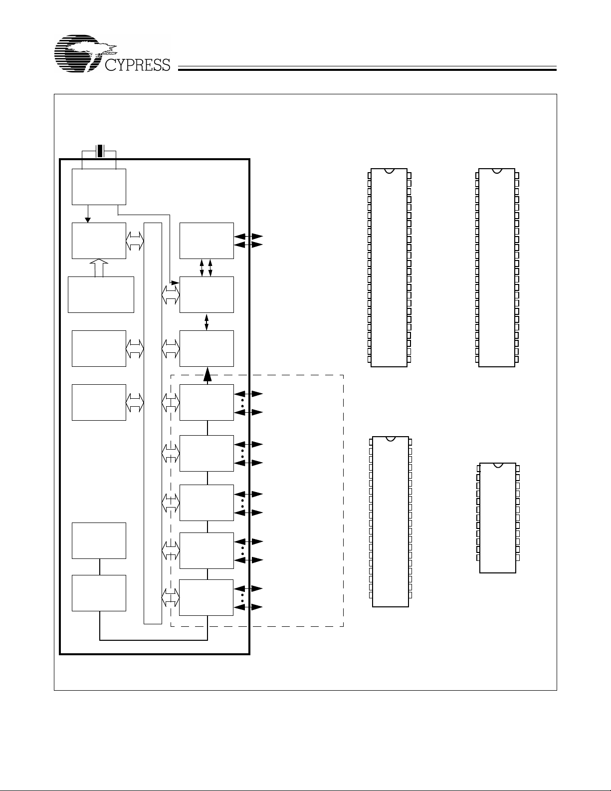
.
Logic Block Diagram
6-MHz ceramic resonator
OSC
12 MHz
4/6/8 Kbyte
6 MHz
12-MHz
8-bit
CPU
EPROM
RAM
256 byte
8-bit Bus
12-bit
Timer
Watch Dog
Timer
Power-on
Reset
USB
Transceiver
USB
SIE
Interrupt
Controller
GPIO
PORT 0
GPIO
PORT 1
GPIO
PORT 2
GPIO
PORT 3
DAC
PORT
D+
D–
TOP VIEW
P0[0]
P0[7]
P1[0]
P1[7]
P2[0]
P2[7]
P3[0]
P3[7]
DAC[0]
DAC[7]
USB
PS/2
PORT
See Note 1
High Current
Outputs
Pin Configuration
48-pin SSOP
1
D+
D–
P3[7]
P3[5]
P3[3]
P3[1]
P2[7]
P2[5]
P2[3]
P2[1]
P1[7]
P1[5]
P1[3]
P1[1]
DAC[7]
DAC[5]
P0[7]
P0[5]
P0[3]
P0[1]
DAC[3]
DAC[1]
V
PP
Vss
CY7C63411/12/13
40-pin PDIP
40-pin CerDIP
D+
D–
P3[7]
P3[5]
P3[3]
P3[1]
P2[7]
P2[5]
P2[3]
P2[1]
P1[7]
P1[5]
P1[3]
P1[1]
P0[7]
P0[5]
P0[3]
P0[1]
V
PP
Vss
48
2
47
3
46
4
45
5
44
43
6
7
42
8
41
9
40
10
39
11
38
12
37
13
36
35
14
15
34
16
33
17
32
18
31
19
30
20
29
21
28
22
27
23
26
24 25
40
1
39
2
38
3
37
4
36
5
35
6
34
7
33
8
32
9
31
10
30
11
29
12
28
13
27
14
26
15
25
16
24
17
23
18
19
22
20
21
TOP VIEW
V
CC
Vss
P3[6]
P3[4]
P3[2]
P3[0]
P2[6]
P2[4]
P2[2]
P2[0]
P1[6]
P1[4]
P1[2]
P1[0]
DAC[6]
DAC[4]
P0[6]
P0[4]
P0[2]
P0[0]
DAC[2]
DAC[0]
XTAL
XTAL
V
CC
V
SS
P3[6]
P3[4]
P3[2]
P3[0]
P2[6]
P2[4]
P2[2]
P2[0]
P1[6]
P1[4]
P1[2]
P1[0]
P0[6]
P0[4]
P0[2]
P0[0]
XTAL
XTAL
OUT
IN
OUT
IN
48-pin SSOP
48-pin SideBraze48-pin SideBraze
1
D+
2
D–
3
P3[7]
4
P3[5]
5
P3[3]
6
P3[1]
7
P2[7]
P2[5]
8
9
P2[3]
10
P2[1]
11
P1[7]
P1[5]
12
13
P1[3]
14
P1[1]
15
NC
16
NC
17
P0[7]
18
P0[5]
19
P0[3]
20
P0[1]
NC
21
NC
22
V
23
PP
Vss
24 25
CY7C63612/13
24-pin SOIC
1
D+
2
D–
3
P3[7]
4
P3[5]
5
P1[3]
6
P1[1]
7
P0[7]
P0[5]
9
P0[3]
10815
P0[1]
11
V
PP
12
Vss
TOP VIEW
48
V
CC
Vss
47
46
P3[6]
P3[4]
45
P3[2]
44
P3[0]
43
P2[6]
42
P2[4]
41
P2[2]
40
39
P2[0]
38
P1[6]
37
P1[4]
36
P1[2]
35
P1[0]
34
NC
33
NC
P0[6]
32
31
P0[4]
30
P0[2]
29
P0[0]
NC
28
NC
27
XTAL
26
24
23
22
21
20
19
18
17
16
14
13
XTAL
V
CC
V
SS
P3[6]
P3[4]
P1[2]
P1[0]
P0[6]
P0[4]
P0[2]
P0[0]
XTAL
XTAL
OUT
IN
OUT
IN
Note:
1. CY7C63612/13 is not bonded out for all GPIO pins shown in Logic Block Diagram. Refer to pin configuration diagram for bonded out pins. See note on page 17
for firmware code needed for unused GPIO pins.
Document #: 38-08027 Rev. ** Page 7 of 36

FOR
FOR
CY7C63411/12/13
CY7C63511/12/13
CY7C63612/13
3.0 Pin Assignments
CY7C63411/12/13
Name I/O
D+, D– I/O 1,2 1,2 1,2 1,2 USB differential data; PS/2 clock and data signals
P0[7:0]
P1[3:0]
P2
P3[7:4]
DAC I/O n/a n/a 15,34,16,
XTAL
IN
XTAL
OUT
V
PP
V
CC
Vss 20,39 24,47 24,47 12,23 Ground
15,26,16,
25,17,24,
I/O
I/O
I/O
I/O
IN 21 25 25 13 6-MHz ceramic resonator or external clock input
OUT 22 26 26 14 6-MHz ceramic resonator
18,23
11,30,12,
29,13,28,
14,27
7,34,8,
33,9,32,
10,31
3,38,4,
37,5,36,
6,35
19 23 23 11 Programming voltage supply, ground during operation
40 48 48 24 Voltage supply
17,32,18,
31,19,30,
20,29
11,38,12,
37,13,36,
14,35
7,42,8,
41,9,40,
10,39
3,46,4,
45,5,44,
6,43
CY7C635
11/12/13
17,32,18,
31,19,30,
20,29
11,38,12,
37,13,36,
14,35
7,42,8,
41,9,40,
10,39
3,46,4,
45,5,44,
6,43
33,21,28,
22,27
CY7C636
12/13
Description40-Pin 48-Pin 48-Pin 24-Pin
7,18,8,
17,9,16,
10,15
5,20,6,19GPIO Port 1 capable of sink ing 7 mA (typical). P1[7:4] not
n/a GPIO Port 2 not bonded out on CY7C63612/13. See
3,22,4,21GPIO Port 3 capable of sinking 12 mA (typical). P3[3:0]
n/a DAC I/O Port with programmable current sink outputs.
GPIO port 0 capable of sinking 7 mA (typical)
bonded out on CY7C63612/13. See note on page 17
for firmware code needed for unused pins.
note on page 17 for firmware code needed for unused
pins.
not bonded out on CY7C63612/13. See note on
page 17 for firmware code needed for unused pins.
DAC[1:0] offer a programmable range of 3.2 to 16 mA
typical. DAC[7:2] have a programmable sink current
range of 0.2 to 1.0 mA ty pi ca l. D AC I/O Port not bonded
out on CY7C63612/13. See not e on page 17 for firmware
code needed for unused pins.
4.0 Programming Model
4.1 14-bit Program Counter (PC)
The 14-bit Program Counter (PC) allows access for up to 8 kilobytes of EPROM using the CY7C634XX/5XX/6XX architecture.
The program counter is cleared during reset, such that the first instruction executed after a reset is at address 0x0000h. This is
typically a jump instruction to a reset handler that initializes the application.
The lower eight bits of the program counter are incremented as instructions are loaded and executed. The upper six bits of the
program counter are increm ented by exe cuting an XPAGE instr uction . As a result, the la st instruc tion execu ted within a 256 -byte
“page” of sequential code should be an XPAGE instruction. The assembler directive “XPAGEON” will cause the assembler to
insert XPAGE instructions automatically. As instructions can be either one or two bytes long, the assembler may occasionally
need to insert a NOP followed by an XPAGE for correct execution.
The program counter of the next instructio n to be executed, ca rry flag, and zero fla g are saved as two bytes on the program sta ck
during an interrupt acknowledge or a CALL instruction. The program counter, carry flag, and zero flag are restored from the
program stack only during a RETI instruction.
Please note the program counter cannot be accessed directly by the firmware. The program stack can be examined by reading
SRAM from location 0x00 and up.
4.2 8-bit Accumulator (A)
The accumulator is the general purpose, do everything register in the architecture where results are usually calculated.
4.3 8-bit Index Register (X)
The index register “X” is available to the firmware as an auxiliary a ccumulator . The X regist er also allow s the processo r to perform
indexed operations by loading an index value into X.
Document #: 38-08027 Rev. ** Page 8 of 36

FOR
FOR
CY7C63411/12/13
CY7C63511/12/13
CY7C63612/13
4.4 8-bit Program Stack Pointer (PSP)
During a reset, the Progra m Stac k Pointer (PSP) is s et to z ero. This mean s the program “stack” starts at RAM addre ss 0x 00 an d
“grows” upward from there. Note the program stack pointe r is directly addressable under firmware co ntrol, usin g the MOV PSP,A
instruction. The PSP supports interrupt service under hardware control and CALL, RET, and RETI instructions under firmware
control.
During an interrupt acknowledge, interrupts are disabled and the 14-bit program counter, carry flag, and zero flag are written as
two bytes of data memory. The first byte is stored in the memory addressed by the program stack pointer, then the PSP is
incremented. The second byte is stored in memory addressed by the program stack pointer and the PSP is incremented again.
The net effect i s t o s tore the prog ram co unt er an d fl ags on the program “stack” and increment the program stack pointer by two.
The Return From Interrupt (RETI) instruction dec rements th e program stack po inter , th en restores th e second byte from memory
addressed by the PSP. The program stack pointer is decremented again and the first byte is restored from memory addressed
by the PSP. After the program counter and flags have been restore d from stack, the interrupts are enabled. The ef fect is to restore
the program counter and flags from the program stack, decrement the program stack pointer by two, and re-enable interrupts.
The Call Subroutine (CALL) in struction stores the program counter and flags on the progra m stack and increments the PSP b y two.
The Return From Subroutine (RET) instruction restores the program counter, but not the flags, from program stack and decre-
ments the PSP by two.
4.5 8-bit Data Stack Pointer (DSP)
The Data Stack Pointer (DSP) supports PUSH and POP instructions that use the data stack for temporary storage. A PUSH
instruction will pre-decremen t the DSP, then wri te data to the memory locatio n address ed by the DSP. A POP instruction will rea d
data from the memory location addressed by the DSP, then post-increment the DSP.
During a reset, the Data Stack Pointer will be set to zero. A PUSH instruction when DSP equal zero will write data at the top of
the data RAM (address 0xFF). This would write data to the memory area reserved for a FIFO for USB endpoint 0. In non-USB
applications, this works fine and is not a proble m. For USB ap plicat ions, it is strong ly recomm ended th at the DSP is load ed aft er
reset just below the USB DMA buffers.
4.6 Address Modes
The CY7C63612/13 microcontrollers support three addressing modes for instructions that require data operands: data, direct,
and indexed.
4.6.1 Data
The “Data” addre ss mode refers to a data ope rand that is actual ly a constant encod ed in the instructi on. As an example, cons ider
the instruction that loads A with the constant 0xE8h:
• MOV A,0E8h
This instruction will require two bytes of code where the first byte identifies the “MOV A” instruction with a data operand as the
second byte. The second byte of the instruction will be the constant “0xE8h”. A constant may be referred to by name if a prior
“EQU” statement assigns the constant value to the name. For example, the following code is equivalent to the example shown
above:
• DSPINIT: EQU 0E8h
• MOV A,DSPINIT
4.6.2 Direct
“Direct” address mode is used when the data operand is a variable stored in SRAM. In that case, the one byte address of the
variable is encoded in the instruction. As an example, consider an instruction that loads A with the contents of memory address
location 0x10h:
• MOV A, [10h]
In normal usage, variable names are assigned to variable addresses using “EQU” statements to improve the readability of the
assembler source code. As an example, the following code is equivalent to the example shown above:
• buttons: EQU 10h
• MOV A,[buttons]
4.6.3 Indexed
“Indexed” address mode allows the firmware to manipulate arrays of data stored in SRAM. The address of the data operand is
the sum of a constant encoded in the instruction and the contents of the “X” register. In normal usage, the constant will be the
“base” address of an array of data and the X register will contain an index that indicates which element of the array is actually
addressed:
Document #: 38-08027 Rev. ** Page 9 of 36

FOR
FOR
CY7C63411/12/13
CY7C63511/12/13
CY7C63612/13
• array: EQU 10h
• MOV X,3
• MOV A,[x+array]
This would have the effect of loading A with the fourth element of the SRAM “array” that begins at address 0x10h. The fourth
element would be at address 0x13h.
Document #: 38-08027 Rev. ** Page 10 of 36

FOR
FOR
CY7C63411/12/13
CY7C63511/12/13
CY7C63612/13
5.0 Instruction Set Summary
MNEMONIC operand opcode cycles MNEMONIC operand opcode cycles
HAL T 00 7 NOP 20 4
ADD A,expr data 01 4 INC A acc 21 4
ADD A,[expr] direct 02 6 INC X x 22 4
ADD A,[X+expr] index 03 7 INC [expr] direct 23 7
ADC A,expr data 04 4 INC [X+expr] index 24 8
ADC A,[expr] direct 05 6 DEC A acc 25 4
ADC A,[X+expr] index 06 7 DEC X x 26 4
SUB A,expr data 07 4 DEC [expr] direct 27 7
SUB A,[expr] direct 08 6 DEC [X+expr] index 28 8
SUB A,[X+expr] index 09 7 IORD expr address 29 5
SBB A,expr data 0A 4 IOWR expr address 2A 5
SBB A,[expr] direct 0B 6 POP A 2B 4
SBB A,[X+expr] index 0C 7 POP X 2C 4
OR A,expr data 0D 4 PUSH A 2D 5
OR A,[expr] direct 0E 6 PUSH X 2E 5
OR A,[X+expr] index 0F 7 SWAP A,X 2F 5
AND A,expr data 10 4 SWAP A,DSP 30 5
AND A,[expr] direct 11 6 MOV [expr],A direct 31 5
AND A,[X+expr] index 12 7 MOV [X+expr],A index 32 6
XOR A,expr data 13 4 OR [expr],A direct 33 7
XOR A,[expr] direct 14 6 OR [X+expr],A index 34 8
XOR A,[X+expr] index 15 7 AND [expr],A direct 35 7
CMP A,expr data 16 5 AND [X+expr],A index 36 8
CMP A,[expr] direct 17 7 XOR [expr],A direct 37 7
CMP A,[X+expr] index 18 8 XOR [X+expr],A index 38 8
MOV A,expr data 19 4 IOWX [X+expr] index 39 6
MOV A,[expr] direct 1A 5 CPL 3A 4
MOV A,[X+expr] index 1B 6 ASL 3B 4
MOV X,expr data 1C 4 ASR 3C 4
MOV X,[expr] direct 1D 5 RLC 3D 4
reserved 1E RRC 3E 4
XPAGE 1F 4 RET 3F 8
MOV A,X 40 4 DI 70 4
MOV X,A 41 4 EI 72 4
MOV PSP,A 60 4 RETI 73 8
CALL addr 50-5F 10
JMP addr 80-8F 5 JC addr C0-CF 5
CALL addr 90-9F 10 JNC addr D0-DF 5
JZ addr A0-AF 5 JACC addr E0-EF 7
JNZ addr B0-BF 5 INDEX addr F0-FF 14
Document #: 38-08027 Rev. ** P age 11 of 36

FOR
FOR
6.0 Memory Organization
6.1 Program Memory Organization
after reset Address
14-bit PC 0x0000 Program execution begins here after a reset
CY7C63411/12/13
CY7C63511/12/13
CY7C63612/13
0x0002 USB Bus Reset interrupt vector
0x0004 128-µs timer interrupt vector
0x0006 1.024-ms timer interrupt vector
0x0008 USB address A endpoint 0 interrupt vector
0x000A USB address A endpoint 1 interrupt vector
0x000C USB address A endpoint 2 interrupt vector
0x000E Reserved
0x0010 Reserved
0x0012 Reserved
0x0014 DAC interrupt vector
0x0016 GPIO interrupt vector
0x0018 Reserved
0x001A Program Memory begins here
0x0FFF
0x17FF 6-KB PROM ends here (CY7C63612)
(8K - 32 bytes)
0x1FDF 8-KB PROM ends here (CY7C63613)
Figure 6-1. Program Memory Space with Interrupt Vector Table
Document #: 38-08027 Rev. ** Page 12 of 36

FOR
FOR
CY7C63411/12/13
CY7C63511/12/13
CY7C63612/13
6.2 Data Memory Organization
The CY7C63612/13 microcontrollers provide 256 bytes of data RAM. In normal usage, the SRAM is partitioned into four areas:
program stack, data stack, user var iab les and USB end poi nt FIFO s as sho w n belo w:
after reset Address
8-bit PSP 0x00 Program Stack begins here and grows upward
8-bit DSP user Data Stack begins here and grows downward
The user determines the amount of memory required
User Variables
0xE8
USB FIFO for Address A endpoint 2
0xF0
0xF8
To p of RAM Memory 0xFF
USB FIFO for Address A endpoint 1
USB FIFO for Address A endpoint 0
Document #: 38-08027 Rev. ** Page 13 of 36

FOR
FOR
CY7C63411/12/13
CY7C63511/12/13
CY7C63612/13
6.3 I/O Register Summary
I/O registers are accessed via the I/O Read (IO RD) and I/O W ri te (IOWR, IOW X) instru ction s. IORD reads the selecte d port into
the accumulator. IOWR writes data from the accumulator to the selected port. Indexed I/O Write (IOWX) adds the contents of X
to the address in the instruction to form the port address and writes data from the accumulator to the specified port. Note that
specifying address 0 (e.g., IOWX 0h) means the I/O port is selected solely by the contents of X.
Table 6-1. I/O Register Summary
Register Name I/O Address Read/Write Function
Port 0 Data 0x00 R/W GPIO Port 0
Port 1 Data 0x01 R/W GPIO Port 1
Port 2 Data 0x02 R/W GPIO Port 2
Port 3 Data 0x03 R/W GPIO Port 3
Port 0 Interrupt Enable 0x04 W Interrupt enable for pins in Port 0
Port 1 Interrupt Enable 0x05 W Interrupt enable for pins in Port 1
Port 2 Interrupt Enable 0x06 W Interrupt enable for pins in Port 2
Port 3 Interrupt Enable 0x07 W Interrupt enable for pins in Port 3
GPIO Configuration 0x08 R/W GPIO Ports Configurations
USB Device Address A 0x10 R/W USB Device Address A
EP A0 Counter Register 0x11 R/W USB Address A, Endpoint 0 counter register
EP A0 Mode Register 0x12 R/W USB Address A, Endpoint 0 configuration register
EP A1 Counter Register 0x13 R/W USB Address A, Endpoint 1 counter register
EP A1 Mode Register 0x14 R/C USB Address A, Endpoint 1 configuration register
EP A2 Counter Register 0x15 R/W USB Address A, Endpoint 2 counter register
EP A2 Mode Register 0x16 R/C USB Address A, Endpoint 2 configuration register
USB Status & Control 0x1F R/W USB upstream port traffic status and control register
Global Interrupt Enable 0x20 R/W Global interrupt enable register
Endpoint Interrupt Enable 0x21 R/W USB endpoint interrupt enables
Timer (LSB) 0x24 R Lower eight bits of free-running timer (1 MHz)
Timer (MSB) 0x25 R Upper four bits of free-runn ing time r tha t are la tch ed
WDR Clear 0x26 W Watch Dog Reset clear
DAC Data 0x30 R/W DAC I/O
DAC Interrupt Enable 0x31 W Interrupt enable for each DAC pin
DAC Interrupt Polarity 0x32 W Interrupt polarity for each DAC pin
DAC Isink 0x38-0x3F W One four bit sink current register for each DAC pin
Processor Status & Control 0xFF R/W Microprocessor status and control
Note:
2. DAC I/O Port not bonded out on CY7C63612/13. See note on page 17 for firmware code needed for unused GPIO pins.
when the lower eight bits are read.
[2]
[2]
[2]
[2]
Document #: 38-08027 Rev. ** Page 14 of 36

FOR
FOR
CY7C63411/12/13
CY7C63511/12/13
CY7C63612/13
7.0 Clocking
Clock Distribution
clk1x
(to USB SIE)
clk2x
(to Microcontroller)
Clock
Doubler
30 pF
30 pF
Figure 7-1. Clock Oscillator On-chip Circuit
The XTALIN and XTAL
external oscillator can be connected to these pins to provide a reference frequency for the internal clock distribution and clock
are the clock pins to the microcontroller. The user can connect a low-cost ceramic resonator or an
OUT
doubler.
An external 6 MHz clock can be applied to th e XT AL
pin is not permissible as the internal clock is effectively shorted to ground.
pin if the XTAL
IN
pin is left open. Please note that grounding the XT AL
OUT
XTALOUT
XTALIN
OUT
8.0 Reset
The USB Controller supp orts three types of re sets. All registe rs are restored to t heir default state s during a reset. The USB Device
Addresses are set to 0 and all inte rrupts are disabled. In ad dition, the Program Stack Po inter (PSP) and Data Stack Pointer (DSP)
are set to 0x00. For USB applications, the firmware should set the DSP below 0xE8h to avoid a memory conflict with RAM
dedicated to USB FIFOs. The assembly instructions to do this are shown below:
Mov A, E8h ; Move 0xE8 hex into Accumulator
Swap A,dsp ; Swap accumulator value int o dsp register
The three reset types are:
1. Power-On Reset (POR)
2. Watch Dog Reset (WDR)
3. USB Bus Reset (non hardware reset)
The occurrence of a res et is rec orde d i n t he Proc es sor Stat us and Control Register l ocate d a t I/O a ddre ss 0 xFF. Bits 4, 5, and 6
are used to record the occurrence of POR, USB Reset, and WDR respectively. The firmware can interrogate these bits to
determine the cause of a reset.
The microcontroller begins execution from ROM address 0x0000h after a POR or WDR reset. Although this looks like interrupt
vector 0, there is an important difference. Reset processing does NOT push the program counter, carry flag, and zero flag onto
program stack. That means the reset handler in firmware should initialize the hardware and begin executing the “main” loop of
code. Attempting to execute either a RET or RETI in the reset handler will cause unpredictable execution results.
8.1 Power-On Reset (POR)
Power-On Reset (POR) occurs every time the VCC voltage to the device ramps from 0V to an internal ly define d trip volta ge (V rst)
of approximately 1/2 full supply voltage. In addition to the normal reset initialization noted under “Reset,” bit 4 (PORS) of the
Processor Status and Control Register is set to “1” to indicate to the firmware that a Power-On Reset occurred. The POR event
forces the GPIO p orts i nto i npu t m od e (hig h im ped anc e), an d the s tate o f Po rt 3 b it 7 is us ed to c on trol ho w the part will respond
after the POR releases.
If Port 3 bit 7 is HIGH (pulled to V
permanent power down/suspend mode, waiting for the USB IO to go to one of Bus Reset, K (resume) or SE0. If Port 3 bit 7 is
still HIGH when the part comes out of suspend, then a 128-µs timer starts, delaying CPU operation until the ceramic resonator
has stabilized.
If Port 3 bit 7 was LOW (pulled to V
continuing to run as reset.
Firmware should clear the POR Status (PORS) bit in register FFh before going into suspend as this status bit selects the 128-µs
or 96-ms start-up timer value as follows: IF Port 3 bit 7 is HIGH then 128-µs is always used; ELSE if PORS is HIGH then 128-ms
is used; ELSE 128-µs is used.
) and the USB IO are at the idle state (DM HIGH and DP LOW) the part will go into a semi-
CC
) the part will start a 96-ms timer, delaying CPU operation until VCC has stabili zed, th en
SS
Document #: 38-08027 Rev. ** Page 15 of 36

FOR
FOR
CY7C63411/12/13
CY7C63511/12/13
CY7C63612/13
8.2 Watch Dog Reset (WDR)
The Watc h Dog T imer Reset (WDR) occur s when the Most Signific ant Bit (MSB) o f the 2-bit W atch Dog T imer Regist er transition s
from LOW to HIGH. In addition to the normal reset initialization noted under “Reset,” bit 6 of the Processor Status and Control
Register is set to “1” to indicate to the firmware that a Watch Dog Reset occurred.
8.192 ms
to 14.336 ms
2.048 ms
At least 8.192 ms
since last write to WDT
WDR goes high
for 2.048 ms
Execution begins at
Reset Vector 0X00
Figure 8-1. Watch Dog Reset (WDR)
The Watch Dog Timer is a 2-bit timer clocked by a 4.096-ms clock (bit 11) from the free-running timer. Writing any value to the
write-only Watch Dog Clear I/O port (0x26h) will clear the Wa tch Dog Timer.
In some applications , th e Watch Dog Timer may be cleared in the 1 .02 4-m s ti me r inte rrup t service routine. If the 1.024-m s tim er
interrupt se r vi ce ro ut i n e do es not ge t ex ec u ted f o r 8. 1 9 2 ms or m o re , a Watch D o g Timer R es et w i l l oc cu r. A Watch Dog Timer
Reset lasts for 2.048 ms after which the microcontroller begins execution at ROM address 0x0000h. The USB transmitter is
disabled by a Watch Dog Reset because the USB Device Address Register is cleared. Otherwise, the USB Controller would
respond to all address 0 transactions. The USB transmitter remains disabled until the MSB of the USB address register is set.
9.0 General Purpose I/O Ports
V
Internal
Data Bus
GPIO
CFG
Port Write
Internal
Buffer
Data
Out
Latch
mode
2 bits
Control
Q1
7 kΩ
Q2
CC
Q3
ESD
GPIO
Pin
Port Read
Interrupt
Enable
Control
to Interrupt
Controller
Figure 9-1. Block Diagram of a GPIO Line
Ports 0 to 2 provide 24 GPIO pins that can be read or written. Each port (8 bits) can be configured as inputs with internal pullups, open drain outputs, or traditional CMOS outputs. Please note an open drain output is also a high-impedance (no pull-up)
input. All of the I/O pins within a gi ven port have the same conf iguration. Ports 0 to 2 are con sidered low curren t drive with typical
current sink capability of 7 mA.
The internal pull-up resis tors are typically 7 kΩ. Two fac tors gov ern the enablin g and d isabling of the internal pull-up resisto rs: the
port configuration selected in the GPIO Configuration register and the state of the output data bit. If the GPIO Configuration
selected is “Resistive” and the output data bit is “1,” then the internal p ull-up re sisto r is ena bled for t hat GPIO pin. O therwis e, Q1
is turned off and the 7-kΩ pull-up is disabled. Q2 is “ON” to sink current whenever the output data bit is written as a “0.” Q3
Document #: 38-08027 Rev. ** Page 16 of 36

FOR
FOR
CY7C63411/12/13
CY7C63511/12/13
CY7C63612/13
provides “HIGH” source current when the GPIO port is configured for CMOS outputs and the output data bit is written as a “1”.
Q2 and Q3 are sized to sink and source, respectively, roughly the same amount of current to support traditional CMOS outputs
with symmetric drive.
P0[7] P0[6] P0[5] P0[4] P0[3] P0[2] P0[1] P0[0]
P1[7] P1[6] P1[5] P1[4] P1[3] P1[2] P1[1] P1[0]
Figure 9-2. Port 1 Data 0x01h (read/write)
P2[7] P2[6] P2[5] P2[4] P2[3] P2[2] P2[1] P2[0]
Figure 9-3. Port 2 Data 0x02h (read/write)
P3[7] P3[6] P3[5] P3[4] P3[3] P3[2] P3[1] P3[0]
Figure 9-4. Port 3 Data 0x03h (read/write)
Low current outputs
0.2 mA to 1.0 mA typical
DAC[7] DAC[6] DAC[5] DAC[4] DAC[3] DAC[2] DAC[1] DAC[0]
Figure 9-5. DAC Port Data 0x30h (read/write)
Port 3 has eight GPIO pins. Port 3 (8 bits) can be configured as inputs with internal pull-ups, open drain outputs, or traditional
CMOS outputs. An open drain output is also a high-impedance input. Port 3 offers high current drive with a typical current sink
capability of 12 mA. The internal pull-up resistors are typically 7 kΩ.
Note: Special care should be exercised with any unused GPIO data bits. An unused GPIO data bit, either a pin on the chip or a
port bit that is not bonded on a particular package, must no t be l eft fl oa ting when the d ev ic e en ters the s us pe nd s tate . If a G PIO
data bit is left floating, the leakage current caused by the floating bit may violate the suspend current limitation specified by the
USB Specification. I f a ‘1’ is wr itten to the unus ed data bit and the port is confi gur ed with ope n drain ou tputs, the un used d ata bit
will be in an indeterminate state. Therefore, if an unused port bit is programmed in open-drain mode, it must be written with a ‘0.’
Notice that the CY7C63612/13 will always require that data bits P1[7:4], P2[7:0], P3[3:0] and DAC[7:0] be written with a ‘0.’
During reset, all of the GPIO pins are set to output “1” (input) with the internal pull-up enabled. In this state, a “1” will always be
read on that GPIO pin unless an external current sink drives the output to a “0” state. Writ ing a “0” to a GPIO pin enables the
output current sink to ground (LOW) and disables the internal pull-up for that pin.
High current outputs
3.2 mA to 16 mA typical
9.1 GPIO Interrupt Enable Ports
During a reset, GPIO interrupts are disabled by clearing all of the GPIO interrupt enable ports. Writing a “1” to a GPIO Interrupt
Enable bit enables GPIO interrupts from the corresponding input pin.
P0[7] P0[6] P0[5] P0[4] P0[3] P0[2] P0[1] P0[0]
Figure 9-6. Port 0 Interrupt Enable 0x04h (write only)
P1[7] P1[6] P1[5] P1[4] P1[3] P1[2] P1[1] P1[0]
Figure 9-7. Port 1 Interrupt Enable 0x05h (write only)
P2[7] P2[6] P2[5] P2[4] P2[3] P2[2] P2[1] P2[0]
Figure 9-8. Port 2 Interrupt Enable 0x06h (write only)
P3[7] P3[6] P3[5] P3[4] P3[3] P3[2] P3[1] P3[0]
Figure 9-9. Port 3 Interrupt Enable 0x07h (write only)
Document #: 38-08027 Rev. ** Page 17 of 36

FOR
FOR
CY7C63411/12/13
CY7C63511/12/13
CY7C63612/13
9.2 GPIO Configuration Port
Every GPIO port can be programmed as inputs with internal pull-ups, open drain outputs, and traditional CMOS outputs. In addition, the interrupt polarity for each port can be prog rammed. With pos itive inter rupt polarity, a rising edge (“0” to “1”) on an input
pin causes an interrupt. With neg ative polarity, a falling edge (“1” to “0”) on an input p in caus es an in terrupt. As shown in the tabl e
below, when a GPIO port is configured with CMOS outputs, interrupts from that port are disabled. The GPIO Configuration Port
register provides two bits per port to program these features. The possible port configurations are:
Port Configuration bits Pin Interrupt Bit Driver Mode Interrupt Polarity
11 X Resistive 10 0 CMOS Output disabled
10 1 Open Drain disabled
01 X Open Drain 00 X Open Drain + (default)
In “Resistive” mode, a 7-kΩ pull-up resistor is conditionally enabled for al l pins of a GPIO port . The resistor is enabled for any pin
that has been written as a “1.” The resistor is disabled on any pin that has been written as a “0.” An I/O pin w ill b e d riv en h igh
through a 7-kΩ pull-up res ist or w hen a “1” ha s b een wri tte n to th e pi n. O r the output pin will be driven LOW, wi th the pull-up disabled, when a “0” has been written to the pin. An I/O pin that has been written as a “1” can be used as an input pin with an integrated 7-kΩ pull-up resistor. Resistive mode selects a negative (falling edge) interrupt polarity on all pins that have the GPIO
interrupt enabled.
In “CMOS” mode, all pins of the GPIO port ar e outputs that are ac tivel y driven. The current s ource an d sink capa city a re roug hly
the same (symmetric output drive). A CMOS port is not a possible source for interrupts.
A port configured in CMOS mode has interrupt generation disabled, yet the interrupt mask bits serve to control port direction. If
a port’s associated Interrupt Ma sk bits a re cleared, those port b its are str ictly outp uts. If the I nterrupt Mask bit s are set then tho se
bits will be open drain input s. As op en dra in in puts, if their data output values are ‘1’ those port pins will be CMOS inputs (HIGH
Z output).
In “Open Drain” mode the internal pull-up resistor and CMOS driver (HIGH) are both disabled. An I/O pin that has been written
as a “1” can be used as either a hig h-im pe dan ce inp ut o r a th ree-s tat e ou tpu t. An I/O pin that has been wri tten as a “0” will drive
the output LOW. The interrupt polarity for an open drain GPIO port can be selected as either positive (rising edge) or negative
(falling edge).
During reset, all of the bits in the GPIO Configuration Register are written with “0.” This selects the default configuration: Open
Drain output, positive interrupt polarity for all GPIO ports.
7 6 5 4 3 2 1 0
Port 3
Config Bit 1
Document #: 38-08027 Rev. ** Page 18 of 36
Port 3
Config Bit 0
Port 2
Config Bit 1
Port 2
Config Bit 0
Port 1
Config Bit 1
Port 1
Config Bit 0
Port 0
Config Bit 1
Port 0
Config Bit 0

10.0 DAC Port
FOR
FOR
CY7C63411/12/13
CY7C63511/12/13
CY7C63612/13
V
CC
Internal
Data Bus
Interrupt
Enable
Interrupt
Polarity
DAC Write
Internal
Buffer
Data
Out
Latch
DAC Read
Isink
Register
4 bits
Isink
DAC
to Interrupt
Controller
Interrupt Logic
Q1
14 KΩ
DAC
I/O Pin
ESD
Figure 10-1. Block Diagram of DAC Port
The DAC port provides th e CY7C6 3511/12/13 with 8 programmable curren t sink I/O pins . W riting a “1” to a DAC I/O pin di sable s
the output current sink (Isi nk DAC) an d dri ve s the I/O p in H IGH throu gh an int egra t ed 14 Koh m resis tor. When a “0” is written to
a DAC I/O pin, th e Isink DAC is enabled and the pull-up resisto r i s d is abl ed . A “0” output will cause the Isink DAC to sink curre nt
to drive the output LOW. The amount of sink current for the DA C I/O pin is p r og ram mable over 16 values based on t he c ontents
of the DAC Isink Register for that output pin. DAC[1:0] are the two high current outputs that are programmable from a minimum
of 3.2 mA to a maxim um of 16 m A (ty pi ca l). DA C[7 :2] are low current outputs that are p rog ram ma ble from a m in im um of 0 .2 m A
to a maximum of 1.0 mA (typical).
When a DAC I/O bit i s wri tten as a “1,” t he I/O pin is either an outp ut p ulled high th rough t he 14 Ko hm resis tor or an inp ut with a n
internal 14 Kohm pull-up resistor. All DAC port data bits are set to “1” during reset.
Low current outputs
0.2 mA to 1.0 mA typical
High current outputs
3.2 mA to 16 mA typical
DAC[7] DAC[6] DAC[5] DAC[4] DAC[3] DAC[2] DAC[1] DAC[0]
Figure 10-2. DAC Port Data 0x30h (read/write)
10.1 DAC Port Interrupts
A DAC port interrupt can be en abled/disabled for each pin individually . The DAC Port Interrupt Ena ble register provides this feature
with an interrupt mask bit for eac h DAC I/O pi n. Wr itin g a “1” to a bit in this register enables interrupts from the corresponding bit
position. Writing a “0” to a bit in the DAC Port Interrupt Enab le regi ster di sable s inte rrupts fr om the cor respon ding bi t posi tion. Al l
of the DAC Port Interrupt Enable register bits are cleared to “0” during a reset.
DAC[7] DAC[6] DAC[5] DAC[4] DAC[3] DAC[2] DAC[1] DAC[0]
Figure 10-3. DAC Port Interrupt Enable 0x31h (write only)
As an additional benefit, the interrupt polarity for each DAC pin is programmable with the DAC Port Interrupt Polarity register.
Writing a “0” to a bit selects negative polarity (fall ing edge) that will caus e an interrupt (if enable d) if a falling edge transi tion occurs
on the corresponding input pin. Writing a “1” to a bit in this register selects positive po larity (rising edge ) that will cause an in terrupt
(if enabled) if a rising edge tran sition occurs on the correspond ing input pin . All of the DAC Port Inte rrupt Polarity regis ter bits are
cleared during a reset.
DAC[7] DAC[6] DAC[5] DAC[4] DAC[3] DAC[2] DAC[1] DAC[0]
Figure 10-4. DAC Port Interrupt Polarity 0x32h (write only)
Document #: 38-08027 Rev. ** Page 19 of 36

FOR
FOR
CY7C63411/12/13
CY7C63511/12/13
CY7C63612/13
10.2 DAC Isink Registers
Each DAC I/O pin has an associated DAC Isink register to program the output sink current when the output is driven LOW. The
first Isink register (0x38h) controls the current for DAC[0], the second (0x39h) for DAC[1], and so on until the Isink register at
0x3Fh controls the current to DAC[7].
Reserved Isink Value
Isink[3] Isink[2] Isink[1] Isink[0]
Figure 10-5. DAC Port Isink 0x38h to 0x3Fh (write only)
11.0 USB Serial In t e rface Engine (S IE)
The SIE allows the microcontro ller to communicate with the USB hos t. The SIE simplifies the interface be tween the microcontroller
and USB by incorporating hardware that handles the following USB bus activity independently of the microcontroller:
• Bit stuffing/unstuffing
• Checksum generation/checking
• ACK/NAK
• Token type identification
• Address checking
Firmware is required to handle the rest of the USB interface with the following tasks:
• Coordinate enumeration by responding to set-up packets
• Fill and empty the FIFOs
• Suspend/Resume coordination
• Verify and select Data toggle values
11.1 USB Enumeration
The enumeration sequence is shown below:
1. The host computer sends a Setup packet followed by a Data packet to USB address 0 requesting the Device descriptor.
2. The USB Controller decodes the request and retrieves its Device descriptor from the program memory space.
3. The host computer performs a control read sequenc e and the USB Controller responds by sending th e Device de scriptor ove r
the USB bus.
4. After receiving the descriptor, the host computer sends a Setup packet followed by a Data packet to address 0 assigning a
new USB address to the device.
5. The USB Controller stores the new address in its USB Device Address Regis ter after the no-data control sequen ce is complete.
6. The host sends a request for the Device descriptor using the new USB address.
7. The USB Controller decodes the request and retrieves the Device descriptor from the program memory.
8. The host performs a control read sequence and the USB Controller respon ds by sending its Device descriptor over the USB bus .
9. The host generates control reads to the USB Controller to request the Configuration and Report descriptors.
10.The USB Controller retrieves the descriptors from its program space and returns the data to the host over the USB.
11.2 PS/2 Operation
PS/2 operation is possible with the CY7 C634XX/5XX /6XX se ries thro ugh the us e of firmwa re and sev eral operati ng mode s. The
first enabling feature:
1. USB Bus rese t on D+ and D− is an interrupt that can be disabled;
2. USB traffic can be disabled via bit 7 of the USB register;
3. D+ and D− can be monitored and driven via firmware as independent port bits.
Bits 5 and 4 of the Upstream Status and Contro l regi ste r are di rec tly connec ted to the D + an d D− USB pin s of the CY7 C634 XX/
5XX/6XX. These pins constantly monitor the levels of th es e si gna ls with C M OS inpu t thresholds. Firmware can pol l and decode
these signals as PS/2 clock and data.
Bits [2:0] defaults to ‘000’ at res et w hi ch allows the USB SIE to c ontr ol output on D+ and D−. Firmware can override the SIE and
directly control the stat e of the se pins vi a these 3 control b its. Sinc e PS/2 is an open drai n signa ling pro tocol, these mo des allow
all 4 PS/2 states to be generated on the D+ and D− pins
Document #: 38-08027 Rev. ** Page 20 of 36

FOR
FOR
CY7C63411/12/13
CY7C63511/12/13
CY7C63612/13
11.3 USB Port Status and Control
USB status and control is regulated by the USB Status and Control Register located at I/O address 0x1Fh as shown in
Figure 11-1. This is a read/write register. All reserved bits must be written to zero. All bi ts in the re gister ar e cleare d during reset.
7 6 5 4 3 2 1 0
R R R/W R/W R/W R/W
Reserved Reserved D+ D– Bus Activity Control
Bit 2
Figure 11-1. USB Status and Control Register 0x1Fh
The Bus Activity bit is a “sticky” bit that indicates if any non-idle USB event has occurred on the USB bus. The user firmware
should check and clear this bit periodically to detect any loss of bus activity. Writing a “0” to the Bus Activity bit clears it while
writing a “1” preserves the current value. In other words, the firmware can clear the Bus Activity bit, but only the SIE can set it.
The 1.024-ms timer interrupt service routine is normally used to check and clear the Bus Activity bit. The following table shows
how the control bits are encoded for this register.
Control Bits Control action
000 Not forcing (SIE controls driver)
001 Force K (D+ HIGH, D– LOW)
010 Force J (D+ LOW, D– HIGH)
011 Force SE0 (D+ LOW, D– LOW)
100 Force SE0 (D− LOW, D+ LOW)
101 Force D− LOW, D+ HiZ
110 Force D− HiZ, D+ LOW
111 Force D− HiZ, D+ HiZ
Control
Bit 1
Control
Bit 0
12.0 USB Device
USB Device Address A inclu des three end points: EPA0, EPA1, and EP A2 . End Point 0 (EPA0) allows the USB host to recogniz e,
set up, and control the device. In particular, EPA0 is used to receive and transmit control (including set-up) packets.
12.1 USB Ports
The USB Controller provides one USB device address with three endpoints. The USB Device Address Register contents are
cleared during a reset, setting the USB device address to zero and marking this address as disabled. Figure 12-1 shows the
format of the USB Address Register.
Device
Address
Enable
Bit 7 (Device Address Enable) in the USB Device Address Register must be set by firmware before the serial interface engine
(SIE) will respond to USB traffic to this address. The Device Address in bits [6:0] must be set by firmware during the USB enumeration process to an add ress assi gned by the USB host th at do es not equ al zero. This regist er is cle ared by a hardw are res et
or the USB bus reset.
12.2 Device Endpoints (3)
The USB controller communicates with the host using dedicated FIFOs, one per endpoint. Each endpoint FIFO is implemented
as 8 bytes of dedicated SRAM. There are three endpoints defined for Device “A” that are labeled “EPA0,” “EPA1,” and EPA2.”
All USB devices are require d to have an endpoint numb er 0 (EP A0) that is used to initiali ze and control the USB devic e. End Point
0 provides access to the device configuration information and allows generic USB status and control accesses. End Point 0 is
bidirectional as the USB controller can both receive and transmit data.
The endpoint mode registers are cleared during reset. The EPA0 endpoint mode register uses the format shown below:
Device
Address
Bit 6
Device
Address
Bit 5
Figure 12-1. USB Device Address Register 0x10h (read/write)
Device
Address
Bit 4
Device
Address
Bit 3
Device
Address
Bit 2
Device
Address
Bit 1
Device
Address
Bit 0
Document #: 38-08027 Rev. ** Page 21 of 36

FOR
FOR
CY7C63411/12/13
CY7C63511/12/13
CY7C63612/13
Endpoint 0
Set-up
Received
Bits[7:5] in the endpoint 0 mode registers (EPA0) are “sticky” status bits that are set by the SIE to report the type of token that
was most recently received. The sticky bits must be cleared by firmware as part of the USB processing.
The endpoint mode registers for EPA1 and EPA2 do not use bits [7:5] as shown below:
Reserved Reserved Reserved Acknowledge Mode
The ‘Acknowledge’ bit is set whenever the SIE engages in a transaction that completes with an ‘ACK’ packet.
The ‘set-up’ PID status (bit[7]) is forced HIGH from the start of the data packet phase of the set-up transaction, until the start of
the ACK packet returned by the SIE. The CPU is prevented from clearing this bit during this interval, and subsequently until the
CPU first does an IORD to this endpoint 0 mode register.
Bits[6:0] of the endpoint 0 mode register are locked from CPU IOWR operations only if the SIE has updated one of these bits,
which the SIE does onl y at the end of a packet transac ti on (set-up ... Data ... ACK, or Out ... Data ... ACK, or In ... Data ... ACK).
The CPU can unlock these bits by doing a subsequent I/O read of this register.
Firmware must do an IORD after an IOWR to an endpoint 0 register to verify that the contents have changed and that the SIE
has not updated these values.
While the ‘set-up’ bit is set, the CPU cannot write to the DMA buffers at memory locatio ns 0 xE0 thro ug h 0x E7 a nd 0 xF 8 th roug h
0xFF. This prevents an incoming set-up transaction from conflicting with a previous In data buffer filling operation by firmware.
The mode bits (bits [3:0]) in an Endpoint Mode Register control how the endpoint responds to USB bus traffic. The mode bit
encoding is shown in Section 16.0.
The format of the endpoint Device counter registers is shown below:
Endpoint 0
In
Received
Endpoint 0
Out
Received
Acknowledge Mode
Bit 3
Bit 3
Mode
Bit 2
Mode
Bit 2
Mode
Bit 1
Mode
Bit 1
Mode
Bit 0
Mode
Bit 0
Data 0/1
Toggle
Bits 0 to 3 indicate the number of data bytes to be transmitted during an IN packet, valid values are 0 to 8 inclusive. Data Valid
bit 6 is used for OUT and set-up tok ens only . Data 0/1 T oggle bit 7 selects the DAT A packet’s toggle state: 0 for DA TA0, 1 for DAT A1.
Data Valid Reserved Reserved Byte count
Bit 3
Figure 12-2. USB Device Counter Registers 0x11h, 0x13h, 0x15h (read/write)
Byte count
Bit 2
Byte count
Bit 1
Byte count
Bit 0
13.0 12-bit Free-running Timer
The 12-bit timer provides two interrupts (128 µs and 1.024 ms) and allows the firmware to directly time events that are up to
4 ms in duration. The lower 8 bits of the timer can be read directly by the firmware. Reading the lower 8 bits latches the upper
4 bits into a temporary register. When the firmware reads the upper 4 bits of the timer, it is actually reading the count stored in
the temporary register. The effect of this logic is to ensure a stable 12-bit timer value can be read, even when the two reads are
separated in time.
13.1 Timer (LSB)
Timer
Bit 7
13.2 Timer (MSB)
Reserved Reserved Reserved Reserved Timer
Timer
Bit 6
Timer
Bit 5
Timer
Bit 4
Timer
Bit 3
Bit 11
Timer
Bit 2
Timer
Bit 10
Timer
Bit 1
Timer
Bit 9
Timer
Bit 0
Timer
Bit 8
Document #: 38-08027 Rev. ** Page 22 of 36

FOR
FOR
CY7C63411/12/13
CY7C63511/12/13
CY7C63612/13
1.024-ms interrupt
µs interrupt
128-
10 9 7856432
1 011
1-MHz clock
L1 L0L2L3
D3 D2 D1 D0 D7 D6 D5 D4 D3 D2 D1 D0
To Timer Register
8
Figure 13-1. Timer Block Diagram
14.0 Processor Status and Control Register
7 6 5 4 3 2 1 0
R R/W R/W R/W R/W R R/W R/W
IRQ
Pending
Watch Dog
Reset
USB Bus
Reset
Power-on
Reset
Suspend, Wait
for Interrupt
Interrupt
Mask
Single Step Run
The “Run” (bit 0) is m anipulate d by the HALT instruction. When Halt is execut ed, the p roces sor cle ars the run bi t and ha lts at th e
end of the current instruction. The processor remains halted until a reset (Power On or Watch Dog). Notice, when writing to the
processor status and control register, the run bit should always be written as a “1.”
The “Single Step” (bit 1) is provided to support a hardware debugger. When single step is set, the processor will execute one
instruction and halt (clear the run bit). This bit must be cleared for normal operation.
The “Interrupt Mas k” (bit 2) sh ows whet her interrup ts are enabl ed or disabled . The firmw are has no dire ct contro l over this bit as
writing a zero or one to this bit position will have no effect on interrupts. Instructions DI, EI, and RETI manipulate the internal
hardware that controls the state of the interrupt mask bit in the Processor Status and Control Register.
Writing a “1” to “Suspend, Wait for Interrupts” (bit 3) will halt the processor and cause the microcontroller to enter the “suspend”
mode that significantly reduces power consumption. A pending interrupt or bus activity will cause the device to come out of
suspend. After coming out of suspen d, the d evice wil l resume firmwa re execut ion at the in struction followi ng the IOWR which put
the part into suspend. An IOWR that attempts to put the part into suspend will be ignored if either bus activity or an interrupt is
pending.
The “Power-on Reset” (bit 4) is only set to “1” during a power on reset. The firmware can check bi ts 4 and 6 in the reset handler
to determine whether a reset was caused by a Power On condi tion or a W atch D og Ti meout. PORS is used to determ ine suspen d
start-up timer value of 128 µs or 128 ms.
The “USB Bus Rese t” (bit 5) will occu r when a USB bus reset is rec eived. Th e USB Bus Reset is a sing led-ended ze ro (SE0) that
lasts more than 8 microseconds. An SE0 is defined as the condition in which both the D+ line and the D– line are LOW at the
same time. W hen t h e SI E de te c ts t his co nd i ti o n, t h e US B B us Re se t bit i s s et i n th e P roc es so r St a tus an d C ont r ol re gi ste r a nd
an USB Bus Reset interrupt is generated. Please note this is an interrupt to the microcontroller and does not actually reset the
processor.
The “Watch Dog Reset” (bit 6) is set during a reset initiated by the Watch Dog Timer. This indicates the Watch Dog Timer went
for more than 8 ms between watch dog clears.
The “IRQ Pending” (bit 7) indicates one or more of the interrupts has been recognized as active. The interrupt acknowledge
sequence should clear this bit until the next interrupt is detected.
During Power-on Reset, the Proc es so r Statu s a nd C on trol Regi ste r is s et to 000 100 01, which indicates a Power-on Res et (bi t 4
set) has occurred and no interrupts are pending (bit 7 clear) yet.
During a Watch Dog Reset, the Processor Status and Control Register is set to 01000001, which indicates a Watch Dog Reset
(bit 6 set) has occurred and no interrupts are pending (bit 7 clear) yet.
Document #: 38-08027 Rev. ** Page 23 of 36

FOR
FOR
CY7C63411/12/13
CY7C63511/12/13
CY7C63612/13
15.0 Interrupts
All interrupts are maskable by the Global Interrupt Enable Register and the USB End Point Interrupt Enable Register. Writing a
“1” to a bit position enables the interrupt associated wi th that bit pos ition. During a reset, the co ntents the Glo bal Interrupt E nable
Register and USB End Point Interrupt Enable Register are cleared, effectively disabling all interrupts.
7 6 5 4 3 2 1 0
R/W R/W R/W R/W R/W
Reserved Reserved GPIO
Interrupt
Enable
7 6 5 4 3 2 1 0
Reserved Reserved Reserved Reserved Reserved EPA2
Figure 15-1. USB End Point Interrupt Enable Register 0x21h (read/write)
DAC
Interrupt
Enable
Reserved 1.024-ms
Interrupt
Enable
R/W R/W R/W
Interrupt
Enable
128-µsec
Interrupt
Enable
EPA1
Interrupt
Enable
USB Bus RST
Interrupt
Enable
EPA0
Interrupt
Enable
Pending interrupt requests are recognized during the last clock cycle of the current instruction. When servicing an interrupt, the
hardware will first disable all interrupts by clearing the Interrupt Enable bit in the Processor Status and Control Register. Next, the
interrupt latch of the current interrupt is cleared. This is followed by a CALL instruction to the ROM address associated with the
interrupt being servic ed (i.e., the Interrupt V ector). The instructio n in the interrupt tab le is typically a J MP instruction to the address
of the Interrupt Service Routine (ISR). The user can re-enable interrupts in the interrupt service routine by executing an EI
instruction. Interrupts can be nested to a level limited only by the available stack space.
The Program Counter v alue as well as the C arry and Zer o flags (C F, ZF) are automatically stored o nto the Program Stack by the
CALL instruction as part of the interrupt acknowledge process. The user firmware is responsible for insuring that the processor
state is preserved and restored during an interrupt. The PUSH A instruction should be used as the first command in the ISR to
save the accumul ator valu e and the POP A instruc tion sho uld be us ed just before the RETI ins truction to restore the accu mulator
value. The program counter CF and ZF are restored and interrupts are enabled when the RETI instruction is executed.
15.1 Interrupt Vectors
The Interrupt V ec tors supported by the U SB Controller a re listed in Table 15-1. Although Reset is not an interr upt, per se, the first
instruction execut ed after a reset is at PROM address 0x0000 h—which corre sponds to t he first entry in the Interrupt V ector Table.
Because the JMP instruction is 2 bytes long, the interrupt vectors occupy 2 bytes.
Table 15-1. Interrupt Vector Assignments
Interrupt V ecto r Number ROM Address Function
not applicable 0x0000h Execution after Reset begins here
1 0x0002h USB Bus Reset interrupt
2 0x0004h 128-µs timer interrupt
3 0x0006h 1.024-ms timer interrupt
4 0x0008h USB Address A Endpoint 0 interrupt
5 0x000Ah USB Address A Endpoint 1 interrupt
6 0x000Ch USB Address A Endpoint 2 interrupt
7 0x000Eh Reserved
8 0x0010h Reserved
9 0x0012h Reserved
10 0x0014h DAC interrupt
11 0x0016h GPIO interrupt
12 0x0018h Reserved
Document #: 38-08027 Rev. ** Page 24 of 36

FOR
FOR
CY7C63411/12/13
CY7C63511/12/13
CY7C63612/13
15.2 Interrupt Latency
Interrupt latency can be calculated from the following equation:
Interrupt Latency = (Number of clock cycles re ma ini ng in the current instruction) + (10 clock cycles for th e C ALL in stru cti on) +
For example, if a 5 clock cycle instruction such as JC is being executed when an interrupt occurs, the first instruction of the
Interrupt Service Routine will execute a min. of 16 clocks (1+10+5) or a max. of 20 clocks (5+10+5) after the interrupt is issued.
Remember that the interrupt latches are sampled at the rising edge of the last clock cycle in the current instruction.
15.2.1 USB Bus Reset Interrupt
The USB Bus Reset interrupt is asserted when a USB bus reset condition is detected. A USB bus reset is indicated by a single
ended zero (SE0) on the upstream port for more than 8 microseconds.
15.2.2 Timer Interrupt
There are two timer interrupts: the 128-µs interrupt and the 1.024-ms interrupt. The user should disable both timer interrupts
before going into the suspe nd mod e to avo id pos sible confl ict s betwee n serv icing the inte rrupts fi rst or the sus pend re quest first.
15.2.3 USB Endpoint Interrupts
There are three USB endpoint i nterrupts, one pe r endpoint. The USB end points interrup t after the either the USB ho st or the USB
controller sends a packet to the USB.
(5 clock cycles for the JMP instruction)
15.2.4 DAC Interrupt
Each DAC I/O pin can generate an interrupt, if enabled.The interrupt polarity for each DAC I/O pin is programmable. A positive
polarity is a rising edge input while a negative polarity is a falling edge input. All of the DAC pins share a single interrupt vector,
which means the firmware will need to read the DAC port to determine which pin or pins caused an interrupt.
Please note that if one DAC pin triggered an interrupt, no other DAC pins can cause a DAC interrupt until that pin has returned
to its inactive (non-trig ger) state or the c orresponding interrupt enabl e bit is cleared. Th e USB Controller do es not assign in terrupt
priority to different DAC pins and the DAC Interrupt Enable Register is not cleared during the interrupt acknowledge process.
15.2.5 GPIO Interrupt
Each of the 32 GPIO pi ns can genera te an i nterr upt, if e nable d. The i nterrupt polarit y can be pr ogramme d for eac h GPIO port a s
part of the GPIO configuration. All of the GPIO pins share a single interrupt vector, which means the firmware will need to read
the GPIO ports with enabled interrupts to determine which pin or pins caused an interrupt.
Please note that if one port pin triggered an int errupt, no other port pins can cause a GPIO interrupt until that port pin has returned
to its inactive (non-trigger) state or its corresponding port interrupt enable bit is cleared. The USB Controller does not assign
interrupt priority to different port pins and the Port Interrupt Enable Registers are not cleared during the interrupt acknowledge
process.
Document #: 38-08027 Rev. ** Page 25 of 36

FOR
FOR
CY7C63411/12/13
CY7C63511/12/13
CY7C63612/13
16.0 Truth Tables
Table 16-1. USB Register Mode Encoding
Mode Encoding Setup In Out Comments
Disable 0000 ignore ignore ignore Ignore all USB traffic to this endpoint
Nak In/Out
0001
Status Out Only 0010 accept stall check For Control endpoints
Stall In/Out 0011 accept stall stall For Control endpoints
Ignore In/Out 0100 accept ignore ignore For Control endpoints
Isochronous Out
0101
Status In Only 0110 accept TX 0 stall For Control Endpoints
Isochronous In
0111
Nak Out 1000 ignore ignore NAK An ACK from mode 1001 --> 1000
Ack Out 1001 ignore ignore ACK This mode is changed by SIE on issuance of ACK --> 1000
Nak Out - Status
In 1010
Ack Out - Status
In 1011
Nak In 1100 ignore NAK ignore An ACK from mode 1101 --> 1100
Ack In 1101 ignore TX cnt ignore This mode is changed by SIE on issuance of ACK --> 1100
Nak In - Status
Out 1110
Ack In - Status
Out 1111
accept NAK NAK Forced from Set-up on Control endpoint, from modes other
than 0000
ignore ignore always Available to low speed devices, future USB spec
enhancements
ignore TX cnt ignore Available to low speed devices, future USB spec
enhancements
accept TX 0 NAK An ACK from mode 1011 --> 1010
accept TX 0 ACK This mode is changed by SIE on issuance of ACK --> 1010
accept NAK check An ACK from mode 1111 --> 111 Ack In - Status Out
accept TX cnt Check This mode is changed by SIE on issuance of ACK -->1110
The ‘In’ column represents the SIE’s response to the token typ e.
A disabled endpoint will remain such until firmware changes it, and all endpoints reset to disabled.
Any Setup packet t o an enabl ed and acce pting end point wi ll be cha nged by t he SIE to 000 1 (NAKing). Any mode whi ch indic ates
the acceptance of a Setup will acknowledge it.
Most modes that con trol tran sacti ons in volv ing an e nding ACK will be ch anged b y the SI E to a correspon din g mode w hich NAKs
follow on packets.
A Control endpoint has thre e extra status bits for PID (Setup, In and Out), but must be pl ac ed i n the corre ct m ode to fun ction as
such. Also a non-Control endpoint can be made to act as a Control endpoint if it is placed in a non appropriate mode.
A ‘check’ on an Out token during a Status trans action ch ecks to see that the Out is of zero length an d has a Data Toggle (DTOG)
of 1.
Document #: 38-08027 Rev. ** Page 26 of 36

FOR
FOR
CY7C63411/12/13
CY7C63511/12/13
CY7C63612/13
Table 16-2. Decode table forTable 16-3: “Details of Modes for Differing Traffic Conditions”
Properties of incoming packet
Encoding Status bits What the SIE does to Mode bits
PID Status bits Interrupt?
End Point Mode
3 2 1 0 Token count buffer dval DTOG DVAL COUNT
Setup
In
Out
The validity of the received data
The quality status of the DMA buffer
Setup In Out ACK 3 2 1 0 Response Int
The response of the SIE can be summarized as follows:
1. the SIE will only respond to valid transactions, and will ignore non-valid ones;
2. the SIE will generate IRQ when a valid transaction is completed or when the DMA buffer is corrupted
3. an incoming Data packet is valid if the count is <= 10 (CRC inclusive) and passes all error checking;
4. a Setup will be ignored by all non-Control endpoints (in appropriate modes);
5. an In will be ignored by an Out configured endpoint and vice versa.
End Point
Mode
The In and Out PID status is updated at the end of a transaction.
The Setup PID status is updated at the beginning of the Data packet phase.
The entire EndPoint 0 mode and the Count register are locked to CPU writes at the end of any transaction in which an ACK is
transferred. These registers are only unlocked upon a CPU read of these registers, and only if that read happens after the
transaction completes. This represents about a 1-µs window to which to the CPU is locked from register writes to these USB
registers. Normally the firmware does a registe r read at th e beginni ng of the ISR to u nlock and get the mod e register info rmation.
The interlock on the Mode and Count reg is ters e ns ures th at the fi rmw a re r eco gn ize s the c hanges that the SIE migh t h av e m ad e
during the previous transaction.
Document #: 38-08027 Rev. ** Page 27 of 36

FOR
FOR
CY7C63411/12/13
CY7C63511/12/13
CY7C63612/13
Table 16-3. Details of Modes for Differing Traffic Conditions
End Point Mode PID Set End Point Mode
3 2 1 0 token count buffer dval DTOG DVAL COUNT Setup In Out ACK 3 2 1 0 response int
Setup Packet (if accepting)
See Table 16-1 Setup <= 10 data valid updates 1 updates 1 UC UC 1 0 0 0 1 ACK yes
See Table 16-1 Setup > 10 junk x updates updates updates 1 UC UC UC NoChange ignore yes
See Table 16-1 Setup x junk invalid updates 0 updates 1 UC UC UC NoChange ignore yes
Disabled
0 0 0 0 x x UC x UC UC UC UC UC UC UC NoChange ignore no
Nak In/Out
0 0 0 1 Out x UC x UC UC UC UC UC 1 UC NoChange NAK yes
0 0 0 1 In x UC x UC UC UC UC 1 UC UC NoChange NAK yes
Ignore In/Out
0 1 0 0 Out x UC x UC UC UC UC UC UC UC NoChange ignore no
0 1 0 0 In x UC x UC UC UC UC UC UC UC NoChange ignore no
Stall In/Out
0 0 1 1 Out x UC x UC UC UC UC UC 1 UC NoChange Stall yes
0 0 1 1 In x UC x UC UC UC UC 1 UC UC NoChange Stall yes
Control Write
Normal Out/premature status In
1 0 1 1 Out <= 10 data valid updates 1 updates UC UC 1 1 1 0 1 0 ACK yes
1 0 1 1 Out > 10 junk x updates updates updates UC UC 1 UC NoChange ignore yes
1 0 1 1 Out x junk invalid updates 0 updates UC UC 1 UC NoChange ignore yes
1 0 1 1 In x UC x UC UC UC UC 1 UC 1 NoChange TX 0 yes
NAK Out/premature status In
1 0 1 0 Out <= 10 UC valid UC UC UC UC UC 1 UC NoChange NAK yes
1 0 1 0 Out > 10 UC x UC UC UC UC UC UC UC NoChange ignore no
1 0 1 0 Out x UC invalid UC UC UC UC UC UC UC NoChange ignore no
1 0 1 0 In x UC x UC UC UC UC 1 UC 1 NoChange TX 0 yes
Status In/extra Out
0 1 1 0 Out <= 10 UC valid UC UC UC UC UC 1 UC 0 0 1 1 Stall yes
0 1 1 0 Out > 10 UC x UC UC UC UC UC UC UC NoChange ignore no
0 1 1 0 Out x UC invalid UC UC UC UC UC UC UC NoChange ignore no
0 1 1 0 In x UC x UC UC UC UC 1 UC 1 NoChange TX 0 yes
Control Read
Normal In/premature status Out
1 1 1 1 Out 2 UC valid 1 1 updates UC UC 1 1 NoChange ACK yes
1 1 1 1 Out 2 UC valid 0 1 updates UC UC 1 UC 0 0 1 1 Stall yes
1 1 1 1 Out !=2 UC valid updates 1 updates UC UC 1 UC 0 0 1 1 Stall yes
1 1 1 1 Out > 10 UC x UC UC UC UC UC UC UC NoChange ignore no
1 1 1 1 Out x UC invalid UC UC UC UC UC UC UC NoChange ignore no
1 1 1 1 In x UC x UC UC UC UC 1 UC 1 1 1 1 0 ACK (back) yes
3 2 1 0 token count buffer dval DTOG DVAL COUNT Setup In Out ACK 3 2 1 0 response int
Nak In/premature status Out
1 1 1 0 Out 2 UC valid 1 1 updates UC UC 1 1 NoChange ACK yes
1 1 1 0 Out 2 UC valid 0 1 updates UC UC 1 UC 0 0 1 1 Stall yes
1 1 1 0 Out !=2 UC valid updates 1 updates UC UC 1 UC 0 0 1 1 Stall yes
1 1 1 0 Out > 10 UC x UC UC UC UC UC UC UC NoChange ignore no
1 1 1 0 Out x UC invalid UC UC UC UC UC UC UC NoChange ignore no
1 1 1 0 In x UC x UC UC UC UC 1 UC UC NoChange NAK yes
Status Out/extra In
0 0 1 0 Out 2 UC valid 1 1 updates UC UC 1 1 NoChange ACK yes
0 0 1 0 Out 2 UC valid 0 1 updates UC UC 1 UC 0 0 1 1 Stall yes
Document #: 38-08027 Rev. ** Page 28 of 36

FOR
FOR
CY7C63411/12/13
CY7C63511/12/13
CY7C63612/13
Table 16-3. Details of Modes for Differing Traffic Conditions (continued)
End Point Mode PID Set End Point Mode
3 2 1 0 token count buffer dval DTOG DVAL COUNT Setup In Out ACK 3 2 1 0 response int
0 0 1 0 Out !=2 UC valid updates 1 updates UC UC 1 UC 0 0 1 1 Stall yes
0010Out > 10 UC x UC UC UC UC UCUC UCUCUCUCUC ignore no
0 0 1 0 Out x UC invalid UC UC UC UC UC UC UCUCUCUCUC ignore no
0 0 1 0 In x UC x UC UC UC UC 1 UC UC 0 0 1 1 Stall yes
Out endpoint
Normal Out/erroneous In
1 0 0 1 Out <= 10 data valid updates 1 updates UC UC 1 1 1 0 0 0 ACK yes
1 0 0 1 Out > 10 junk x updates updates updates UC UC 1 UC NoChange ignore yes
1 0 0 1 Out x junk invalid updates 0 updates UC UC 1 UC NoChange ignore yes
1 0 0 1 In x UC x UC UC UC UC UC UC UC NoChange ignore no
NAK Out/erroneous In
1 0 0 0 Out <= 10 UC valid UC UC UC UC UC 1 UC NoChange NAK yes
1 0 0 0 Out > 10 UC x UC UC UC UC UC UC UC NoChange ignore no
1 0 0 0 Out x UC invalid UC UC UC UC UC UC UC NoChange ignore no
1 0 0 0 In x UC x UC UC UC UC UC UC UC NoChange ignore no
Isochronous endpoint (Out)
0 1 0 1 Out x updates updates updates updates updates UC UC 1 1 NoChange RX yes
0 1 0 1 In x UC x UC UC UC UC UC UC UC NoChange ignore no
In endpoint
Normal In/erroneous Out
1 1 0 1 Out x UC x UC UC UC UC UC UC UC NoChange ignore no
1 1 0 1 In x UC x UC UC UC UC 1 UC 1 1 1 0 0 ACK (back) yes
NAK In/erroneous Out
1 1 0 0 Out x UC x UC UC UC UC UC UC UC NoChange ignore no
1 1 0 0 In x UC x UC UC UC UC 1 UC UC NoChange NAK yes
Isochronous endpoint (In)
0 1 1 1 Out x UC x UC UC UC UC UC UC UC NoChange ignore no
0 1 1 1 In x UC x UC UC UC UC 1 UC UC NoChange TX yes
17.0 Absolute Maximum Ratings
Storage Temperature ..........................................................................................................................................–65°C to +150°C
Ambient Temperature with Power Applied...............................................................................................................–0°C to +70°C
Supply Voltage on V
DC Input Voltage........................................................................................................................................... –0.5V to +VCC+0.5V
DC Voltage Applied to Outputs in High Z State ........................................................................................... –0.5V to + VCC+0.5V
Max. Output Current into Port 0,1,2,3 and DAC[1:0] Pins................................................................................................... 60 mA
Max. Output Current into DAC[7:2] Pins............................................................................................................................. 10 mA
Power Dissipation..............................................................................................................................................................300 mW
Static Discharge Voltage .................................................................................................................. ................................ > 2000V
Latch-up Current ........................................................................................................................................................... > 200 mA
Document #: 38-08027 Rev. ** Page 29 of 36
relative to VSS....................................................................................................................–0.5V to +7.0V
CC

FOR
FOR
18.0 DC Characteristics
Fosc = 6 MHz; Operating Temperature = 0 to 70°C
Parameter Min. Max. Unit Conditions
General
V
CC (1)
V
CC (2)
I
CC1
I
CC2
I
SB1
V
PP
T
start
t
int1
t
int2
t
watch
I
il
I
sm
t
vccs
V
oh
V
ol
V
di
V
cm
V
se
C
in
I
lo
R
pu
R
pu
R
pd
R
up
V
ith
V
H
I
ol
I
ol
I
oh
R
up
I
sink0(0)
I
sink0(F)
I
sink1(0)
I
sink1(F)
I
range
Operating Voltage 4.0 5.5 V Non USB activity (note 3)
Operating Voltage 4.35 5.25 V USB activity (note 4)
VCC Operating Supply Current 40 mA V
VCC = 4.35V 15 mA
Supply Current - Suspend Mode 30 µA Oscillator off, D– > Voh min
Programming Voltage (disabled) –0.4 0.4 V
Resonator Start-up Interval 256 µs Vcc = 5.0V, ceramic resonator
Internal Timer #1 Interrupt Period 128 128 µs
Internal Timer #2 Interrupt Period 1.024 1.024 ms
Watch Dog Ti mer Period 8.192 14.33 ms
Input Leakage Current 1 µA Any pin
Max ISS IO Sink Current 60 mA Cumulative across all ports (note 10)
Power-On Reset
VCC Reset Slew 0.001 200 ms Linear ramp: 0 to 4.35V (notes 6,7)
USB Interface
Static Output HIGH 2.8 3.6 V 15k ± 5% ohms to Gnd (note 4)
Static Output LOW 0.3 V
Differential Input Sensitivity 0.2 V |(D+)–(D–)|
Differential Input Common Mode Range 0.8 2.5 V 9-1
Single-Ended Receiver Threshold 0.8 2.0 V
Transceiver Capacitance 20 pF
Hi-Z State Data Line Leakage –10 10 µA0 V < Vin<3.3 V
Bus Pull-up Resistance (VCC option) 7.35K 7.65 kΩ 7.5 kΩ ± 2% to VCC (note 13)
Bus Pull-up Resistance (Ext. 3.3V option) 1.425 1.575 kΩ 1.5 kΩ ± 5% to 3.0–3.6V
Bus Pull-down Resistance 14.25 15.75 kΩ 15 kΩ ± 5%
General Purpose I/O Interface
Pull-up Resistance 4.9K 9.1K Ohms
Input Threshold Voltage 45% 65% V
Input Hysteresis Voltage 6% 12% V
Sink Current 7.2 16.5 mA Port 3, Vout = 1.0V (note 3)
Sink Current 3.5 10.6 mA Port 0,1,2, Vout = 2.0V (note 3)
Source Current 1.4 7.5 mA Voh = 2.4V (all ports 0,1,2,3) (note 3)
DAC Interface
Pull-up Resistance 8.0K 20.0K Ohms (note 14)
DAC[7:2] Sink Current (0) 0.1 0.3 mA Vout = 2.0 V DC (note 4,14)
DAC[7:2] Sink Current (F) 0.5 1.5 mA Vout = 2.0 V DC (note 4,14)
DAC[1:0] Sink Current (0) 1.6 4.8 mA Vout = 2.0 V DC (note 4,14)
DAC[1:0] Sink Current (F) 8 24 mA Vout = 2.0 V DC (note 4,14)
Programmed Isink Ratio: max/min 4 6 Vout = 2.0 V DC (notes 4,11,14)
CY7C63411/12/13
CY7C63511/12/13
= 5.5V
CC
All ports, LOW to HIGH edge
CC
All ports, HIGH to LOW edge
CC
CY7C63612/13
Document #: 38-08027 Rev. ** Page 30 of 36

FOR
FOR
CY7C63411/12/13
CY7C63511/12/13
CY7C63612/13
Parameter Min. Max. Unit Conditions
I
lin
t
sink
T
ratio
19.0 Switching Characteristics
Parameter Description Min. Max. Unit Conditions
t
CYC
t
CH
t
CL
t
r
t
r
t
f
t
f
t
rfm
V
crs
t
drate
t
djr1
t
djr2
t
deop
t
eopr1
t
eopr2
t
eopt
t
udj1
t
udj2
Differential Nonlinearity 0.5 lsb Any pin (note 8,14)
Current Sink Response T im e 0.8 µs Full scale transition (note 14)
Tracking Ratio DAC[1:0] to DAC[7:2] 14 21 Vout = 2.0V (note 9,14)
Clock
Input Clock Cycle Time 165.0 168.3 ns
Clock HIGH Time 0.45 t
Clock LOW Time 0.45 t
CYC
CYC
ns
ns
USB Driver Characteristics
Transition Rise Time 75 ns CLoad = 50 pF
Transition Rise Time 300 ns CLoad = 600 pF
Transition Fall Time 75 ns CLoad = 50 pF
Transition Fall Time 300 ns CLoad = 600 pF
Rise/Fall Time Matching 80 125 % tr/tf
Output Signal Crossover Voltage 1.3 2.0 V
[4, 5]
[4, 5]
[4, 5]
[4, 5]
[4, 5]
[4, 5]
USB Data Timing
Low Speed Data Rate 1.4775 1.5225 Mbs Ave. Bit Rate (1.5 Mb/s ± 1.5%)
Receiver Data Jitter Tolerance –75 75 ns T o Ne xt Transition
Receiver Data Jitter Tolerance –45 45 ns For Paired Transitions
Differential to EOP T ransition Skew –40 100 ns
[10]
EOP Width at Receiver 330 ns Rejects as EOP
EOP Width at Receiver 675 ns Accepts as EOP
[12]
[12]
[12]
[12]
Source EOP Width 1.25 1.50 µs
Differential Driver Jitter –95 95 ns To next transition, Figure 19-5
Differential Driver Jitter –150 150 ns To paired transition, Figure 19-5
Notes:
3. Functionality is guarante ed of the V
4. USB transmitter functionality is guaranteed over the V
5. Per Table 7-7 of revision 1.1 of USB specification, for C
6. Port 3 bit 7 controls whether the parts goes into suspend after a POR event or waits 128 ms to begin running.
7. POR will re-occur whenever V
8. Measured as largest step size vs. nominal according to measured full scale and zero programmed values.
9. T
= Isink1[1:0](n)/Isink0[7:2](n) for the same n, programmed.
ratio
10. Total current cumulative across all Port pins flowing to V
11. Irange: Isinkn(15)/ Isinkn(0) for the same pin.
12. Measured at crossover point of differential data signals.
13. Limits total bus capacitance loading (C
14. DAC I/O Port not bonded out on CY7C63612/13. See note on page 17 for firmware code needed for unused pins.
CC
range, except USB transmitter and DACs.
CC (1)
drops to approximately 2.5V.
) to 400 pF per section 7.1. 5 of revision 1.1 of USB specification.
LOAD
range, as well as DAC outputs.
CC (2)
of 50–600 pF.
LOAD
is limited to minimize Ground-Drop noise effects.
SS
Document #: 38-08027 Rev. ** Page 31 of 36

FOR
FOR
CY7C63411/12/13
CY7C63511/12/13
CY7C63612/13
.
t
CYC
t
CH
CLOCK
t
CL
Figure 19-1. Clock Timing
T
PERIOD
Differential
Data Lines
90%
t
f
10%
t
D+
V
oh
V
crs
V
ol
10%
−
D
r
90%
Figure 19-2. USB Data Signal Timing
T
JR
Consecutive
Transitions
N * T
PERIOD
+ T
JR1
Transitions
N * T
Paired
PERIOD
+ T
T
JR1
JR2
T
JR2
Figure 19-3. Receiver Jitter Tolerance
Document #: 38-08027 Rev. ** Page 32 of 36

T
PERIOD
Differential
Data Lines
T
Differential
Data Lines
PERIOD
FOR
FOR
Crossover
Crossover
Point
Diff. Data to
SE0 Skew
N * T
PERIOD
+ T
DEOP
Point Extended
Source EOP W i dt h: T
Receiver EOP Wi dth: T
Figure 19-4. Differential to EOP Transition Skew and EOP Width
Crossover
Points
CY7C63411/12/13
CY7C63511/12/13
CY7C63612/13
EOPT
, T
EOPR1
EOPR2
Consecutive
Transitions
N * T
PERIOD
+ T
xJR1
Transitions
N * T
Paired
PERIOD
+ T
xJR2
Figure 19-5. Differential Data Jitter
20.0 Ordering Information
Ordering Code
Size
CY7C63411-PC 4 KB P17 40-Pin (600-Mil) PDIP Commercial
CY7C63411-PVC 4 KB O48 48-Lead Shrunk Small Outline Package Commercial
CY7C63412-PC 6 KB P17 40-Pin (600-Mil) PDIP Commercial
CY7C63412-PVC 6 KB O48 48-Lead Shrunk Small Outline Package Commercial
CY7C63413-PC 8 KB P17 40-Pin (600-Mil) PDIP Commercial
CY7C63413-PVC 8 KB O48 48-Lead Shrunk Small Outline Package Commercial
CY7C63511-PVC 4 KB O48 48-Lead Shrunk Small Outline Package Commercial
CY7C63512-PVC 6 KB O48 48-Lead Shrunk Small Outline Package Commercial
CY7C63513-PVC 8 KB O48 48-Lead Shrunk Small Outline Package Commercial
CY7C63612-SC 6 KB S13 24-Pin (300-Mil) SOIC Commercial
CY7C63613-SC 8 KB S13 24-Pin (300-Mil) SOIC Commercial
EPROM
Package
Name Package Type
Operating
Range
Document #: 38-08027 Rev. ** Page 33 of 36

21.0 Package Diagrams
FOR
FOR
48-Lead Shrunk Small Outline Package O48
CY7C63411/12/13
CY7C63511/12/13
CY7C63612/13
40-Lead (600-Mil) Molded DIP P17
51-85061-*C
51-85019-A
Document #: 38-08027 Rev. ** Page 34 of 36

ng so indemnifies Cypress Semiconductor against all charges.
21.0 Package Diagrams (continued)
24-Lead (300-Mil) MoldedSOIC S13
CY7C63411/12/13
CY7C63511/12/13
CY7C63612/13
51-85025-A
Document #: 38-08027 Rev. ** Page 35 of 36
© Cypress Semiconductor Corporation, 2002. The information contained herein is subject to change without notice. Cypress Semiconductor Corporation assumes no responsibility for the use
of any circuitry other than circuitry embodied in a Cypress Semiconductor product. No r does it convey or imply any license under patent or other rights. Cypress Semiconductor does not autho rize
its products for use as critical components in life-support systems where a malfunction or failure may reasonably be expected to result in significant injury to the user. The inclusion of Cypress
Semiconductor products in life-support systems application implies that the manufacturer assume s all risk of such use and in doi

FOR
FOR
CY7C63411/12/13
CY7C63511/12/13
CY7C63612/13
Document Title: CY7C63411/12/13, CY7C63511/12/13, CY7C63612/13 Low-speed USB Peripheral Controller
Document Number: 38-08027
REV. ECN NO.
** 116224 06/12/02 DSG Change from Spec number: 38-00754 to 38-08027
Issue
Date
Orig. of
Change Description of Change
Document #: 38-08027 Rev. ** Page 36 of 36
 Loading...