


查询CY7C63221A供应商查询CY7C63221A供应商
1
enCoRe™ USB
CY7C63221/31A
CY7C63221A/31A
enCoRe™ USB
Low-speed USB Peripheral Controller
Cypress Semiconductor Corporation • 3901 North First Street • San Jose, CA 95134 • 408-943-2600
Document #: 38-08028 Rev. *A Revised October 21, 2002

FOR
FOR
enCoRe™ USB
CY7C63221/31A
TABLE OF CONTENTS
1.0 FEATURES .................................................. .. .. ...................................................... .. .. .....................5
2.0 FUNCTIONAL OVERVIEW ............................................................. .................... .. ................... .......6
2.1 enCoRe USB - The New USB Standard ....................................................................................6
3.0 LOGIC BLOCK DIAGRAM .............................................................................................................7
4.0 PIN CONFIGURATIONS ................................ .. ........................... .. .. .. ........................... .. .. ...............7
5.0 PIN ASSIGNMENTS ............................. ............................... .. ............................... ..........................7
6.0 PROGRAMM I N G M OD E L ....................... .. ............... .. ................ .. .. ................ .. ............... ... .............8
6.1 Program Counter (PC) ...............................................................................................................8
6.2 8-bit Accumulator (A) .................................................................................................................8
6.3 8-bit Index Register (X) .......................................... .................... ................................................8
6.4 8-bit Program Stack Pointer (PSP) ............................................................................................8
6.5 8-bit Data Stack Pointer (DSP) ............... ................................... .................................. ..............9
6.6 Address Modes ..................................... ........................ .. ............................................. ..............9
6.6.1 Data ..................................................................................................................................................9
6.6.2 Direct ................................................................................................................................................9
6.6.3 Indexed ............................................................................................................................................9
7.0 INSTRUCTION SET SUMMARY ................................................... .. ........................... .. .. .. .............10
8.0 MEMORY ORGANIZATION ..........................................................................................................11
8.1 Program Memory Organization ............................... ..................... .................... .................... ....11
8.2 Data Memor y Organization ......... ............... ... ............... .. ................ .. ............... ... ............... .. .....12
8.3 I/O Registe r S u m ma ry ......... ................ .. ............... ... ............... .. ................ .. ............... ... ...........13
9.0 CLOCKING ....................................................................................................................................14
9.1 Internal/External Oscillator Operation ......................................................................................15
9.2 External Oscillator ....................................................................................................................15
10.0 RESET ............................................................ ......................... ............................ ........................16
10.1 Low-volt a g e Re s e t (L V R ) ... .. ................ .. ................ .. .. ............... ... ............... .. ................ .. .......16
10.2 Brown-ou t R e se t (BOR) .............................. .. ............... .. ................ .. .. ................ .. ..................16
10.3 Watchdog Reset (WDR) ....................... .................................................................................17
11.0 SUSPEND MODE ........................................................................................................................17
11.1 Clocking Mode on Wake-up from Suspend ........................... ................................................18
11.2 Wake-up Tim e r ......... ................ .. .. ................ .. ............................... .. ................ .. .. ..................18
12.0 GENERAL PURPOSE I/O PORTS .............................................................................................19
12.1 Auxiliary Input Port .................................................................................................................21
13.0 USB SERIAL INTERFACE ENGINE (SIE) .................................................................................22
13.1 USB Enumeration ..................................................................................................................23
13.2 USB Port Status and Control .................................................................................................23
14.0 USB DEVICE ...............................................................................................................................25
14.1 USB Address Register ...........................................................................................................25
14.2 USB Control Endpoint ............................................................................................................25
14.3 USB Non-Control Endpoints ..................................................................................................26
14.4 USB Endpoint Counter Registers ........................................................ ...................... ............27
Document #: 38-08028 Rev. *A Page 2 of 49

FOR
FOR
enCoRe™ USB
CY7C63221/31A
15.0 USB REGULATOR OUTPUT ......................................................................................................27
16.0 PS/2 OPERATION .......................................................................................................................28
17.0 12-BIT FREE-RUNNING TIMER ......................... .. .......................... ......................... ...................28
18.0 PROCESSOR STATUS AND CONTROL REGISTER ........................................ .. .. ...................29
19.0 INTERRUPTS .................................... .. ......................... .. .. .. .. .......................................................31
19.1 Interrupt Vectors ....................................................................................................................31
19.2 Interrupt Latency ....................................................................................................................32
19.3 Interrupt Sources ...................................................................................................................32
20.0 USB MODE TABLES ..................................................................................................................36
21.0 REGISTER SUMMARY .................................................. .. .. .. .......................................................41
22.0 ABSOLUTE MAXIMUM RATINGS .............................................................................................42
23.0 DC CHARACTERISTICS ............................................................................................................42
24.0 SWITCHING CHARACTERISTICS ............................................. .. .. ............................. .. .............44
25.0 ORDERING INFORMATION .......................................................................................................47
26.0 PACKAGE DIAGRAMS .............................................................................................................47
Document #: 38-08028 Rev. *A Page 3 of 49

FOR
FOR
enCoRe™ USB
CY7C63221/31A
LIST OF FIGURES
Figure 8-1. Pro g ra m M e mory Space with In te rrupt Vector Table ........................... .. ................ .. .........11
Figure 9-1. Clo ck Os cillator On-chip C ir cu it ..... .. .. ................ .. ............... .. ................ .. .. ................ .........14
Figure 9-2. Clo ck C o n fig u r a tion Register (A dd r e ss 0 xF 8 ) .............. .. ............... ................ .. ............... ... 14
Figure 10-1. Watchdog Reset (WDR, Address 0x26) ..........................................................................17
Figure 12-1. Block Diagram of GPIO Port (one pin shown) .................................................................19
Figure 12-2. Port 0 Data (Address 0x 0 0 ) ........... .. ................ .. ............... .. ................ .. ................ .. .........19
Figure 12-3. Port 1 Data (Address 0x 0 1 ) ........... .. ................ .. ............... .. ................ .. ................ .. .........20
Figure 12-4. GPIO Port 0 Mode0 Re gister (Addres s 0 x 0A) ... ............... .. ................ .. ................ ...........20
Figure 12-5. GPIO Port 0 Mode1 Re gister (Addres s 0 x 0B) ... ............... .. ................ .. ................ ...........20
Figure 12-6. GPIO Port 1 Mode0 Re gister (Addres s 0 x 0C) .. .. ............... ... ............... .. ................ .. .......20
Figure 12-7. GPIO Port 1 Mode1 Re gister (Addres s 0 x 0D) .. .. ............... ... ............... .. ................ .. .......21
Figure 12-8. Port 2 Data Register (A d dr e s s 0 x 02 ) .................. .. ................ .. .. ................ .. ............... .. .. .22
Figure 13-1. USB Status and Control Register (Address 0x1F) ..........................................................23
Figure 14-1. USB Device Address Register (Address 0x10) ...............................................................25
Figure 14-2. Endpoint 0 Mode Register (Address 0x12) ................................................................. ....25
Figure 14-3. USB Endpoint EP1 Mode Registers (Address 0x14) ......................................................26
Figure 14-4. Endpoint 0 and 1 Counter Registers (Addresses 0x11 and 0x13) ..................... .............27
Figure 16-1. Diagram of USB - PS/2 System Connections ........................ .. ...................................... .28
Figure 17-1. Timer LSB Register (Address 0x24) ................................................................................29
Figure 17-2. Ti m e r MS B R eg i s te r (A d d ress 0x25) .......... .. ................ .. ................ .. .. ............... ... ...........29
Figure 17-3. Ti m e r Bl o c k D ia g r a m ............................ .. .. ............... ... ............... .. ................ .. .. ................29
Figure 18-1. Processor Status and Control Register (Address 0xFF) .................................................29
Figure 19-1. Global Interrupt Enable Register (Address 0x20) ............................................................32
Figure 19-2. Endpoint Interrupt Enable Register (Address 0x21) ........................ ................................33
Figure 19-3. Interrupt Controller Logic Block Diagram ........................................................................34
Figure 19-4. Port 0 Interrupt Enable Register (Address 0x04) ............................................................34
Figure 19-5. Port 1 Interrupt Enable Register (Address 0x05) ............................................................34
Figure 19-6. Port 0 Interrupt Polarity Register (Address 0x06) ............................................................35
Figure 19-7. Port 1 Interrupt Polarity Register (Address 0x07) ............................................................35
Figure 19-8. GP IO In terrupt Diagra m ..... .. ................ .. ............... .. ................ .. ................ .. ....................35
Figure 24-1. Cl o ck T imi n g ....... ................ .. ................ .. ............... .. ... ............... .. ................ .. ..................45
Figure 24-2. USB Data Signal Timing ..................................................................................................45
Figure 24-3. Rec e iv e r Jitter Toleranc e ... .. ................ .. ............... .. ... ............... .. ................ .. ..................45
Figure 24-4. Di ff erential to EOP Tra n s ition Skew and EOP Wid th .............. .. ................ .. ............... .. ... 46
Figure 24-5. Differential Data Jitter ......................................................................................................46
LIST OF TABLES
Table 8-1. I/O Register Summary .................................... .. ...................... ..................... .......................13
Table 11-1. Wake-up Timer Adjust Settings ........................................................................................18
Table 12-1. Ports 0 and 1 Output Control Truth Table .......................... ...................... ...................... ..21
Table 13-1. Control Modes to Force D+/D– Outputs ...........................................................................24
Table 19-1. Interrupt Vector Assignments ...........................................................................................31
Table 20-1. USB Register Mode Encoding for Control and Non-Control Endpoint ................... ..........36
Table 20-2. Decode table for Table 20-3: “Details of Modes for Differing Traffic Conditions” ............. 38
Table 20-3. Details of Modes for Differing Traffic Co nditions ...................................................... ........39
Table 26-1. CY7C63221A-XC Probe Pad Coordinates in microns ((0,0) to bond pad centers) ..........48
Document #: 38-08028 Rev. *A Page 4 of 49

FOR
FOR
enCoRe™ USB
CY7C63221/31A
1.0 Features
• enCoRe™ USB - enhanced Component Reduction
—Internal oscillator eliminates the need for an external crystal or resonator
—Interface can auto -configure to operate as PS/2 o r USB without the need for externa l components to switc h between
modes (no GPIO pins needed to manage dual mode capability)
—Internal 3.3V regulator for USB pull-up resistor
—Configurable GPIO for real-world interface without external components
• Flexible, cost-effective solution for applications that combine PS/2 and low-speed USB, such as mice, gamepads,
joysticks, and many others
• USB Specification Compliance
—Conforms to USB Specification, Version 2.0
—Conforms to USB HID Specification, Version 1.1
—Supports 1 low-speed USB device address
—Supports 1 control endpoint and 1 data endpoint
—Integrated USB transceiver
—3.3V regulated output for USB pull-up resistor
• 8-bit RISC microcontroller
—Harvard architecture
—6-MHz external ceramic resonator or internal clock mode
—12-MHz internal CPU clock
—Internal memory
—96 bytes of RAM
—3 Kbytes of EPROM
—Interface can auto-configure to operate as PS/2 or USB
—No external components for switching between PS/2 and USB modes
• I/O ports
—Up to 10 versatile General Purpose I/O (GPIO) pins, individually configurable
—High current drive on any GPIO pin: 50 mA/pin current sink
—Each GPIO pin support s high-impedance input s, internal pull-ups, ope n drain outputs, or traditional CMOS outputs
—Maskable interrupts on all I/O pins
—XTALIN, XTALOUT and VREG can be configured as additional input pins
• Internal low-power wake-up timer during suspend mode
—Periodic wake-up with no external components
• Optional 6-MHz internal oscillator mode
—Allows fast start-up from suspend mode
• Watchdog timer (WDT)
• Low-voltage Reset at 3.75V
• Internal brown-out reset for suspend mode
• Improved output drivers to reduce EMI
• Operating voltage from 4.0V to 5.5VDC
• Operating temperature from 0 to 70 degrees Celsius
• CY7C63221A available in DIE form or 16-pin PDIP
• CY7C63231 available in 18-pin SOIC, 18-pin PDIP
• Industry-standard programmer support
Document #: 38-08028 Rev. *A Page 5 of 49

FOR
FOR
enCoRe™ USB
CY7C63221/31A
2.0 Functional Overview
2.1 enCoRe USB - The New USB Standard
Cypress has reinvented its leadership position in the low-speed USB market with a new family of innovative microcontrollers.
Introducing...enCoRe™ USB—“enhanced C ompon ent Reduc tio n.” Cypr ess h as l ev erag ed its design e xp erti se in USB so lutions
to create a new family of low-speed USB microcontrollers that enables peripheral developers to design new products with a
minimum number of components. At the heart of the Cypress enCoRe USB technology is the breakthrough design of a crystalless oscillator. By integrating the oscillator into the chip, an external crystal or resonator is no longer needed. We have also
integrated other ex ternal components commonly found i n low-speed USB appli cations such as pull-up resistors, wa ke-up circuitry ,
and a 3.3V regulator. All of this adds up to a lower system cost.
The CY7C632XX family is comprised of 8-bit RISC One Time Programmable (OTP) microcontrollers. The instruction set has
been optimized specifically for USB and PS/2 operations, although the microcontrollers can be used for a variety of other
embedded applications.
The CY7C632XX features up to 10 general-purpose I/O (GPIO) pins to support USB, PS/2 and other applications. The I/O pins
are grouped into two po rts (Po rt 0 to 1) wh ere each pin can be ind ividu ally c onfigu red as input s with interna l pull-u ps, open drain
outputs, or tr aditional CMOS ou tput s with p rogrammab le drive strength of up to 50 m A output drive. Add itionall y, each I/O pin can
be used to generate a GPIO interrupt to the microcontroller.
The CY7C632XX microcontrollers feature an internal oscillator. With the presence of USB traffic, the internal oscillator can be
set to precisely tune to U SB timing requirement s (6 MHz ± 1.5%). This clock gene rator has been optimize d to reduce clock-relate d
noise emissions (EMI), and provides the 6-MHz and 12-MHz clocks that remain internal to the microcontroller. When using the
internal oscillator, XTALIN and XTALOUT can be configured as additional input pins that can be read on port 2. Optionally, an
external 6-MHz ceramic resonator can be used to provide a higher precision reference if needed.
The CY7C632XX is offered with 3 Kbytes of EPROM to minimize cost, and has 96 bytes of data RAM for stack space, user
variables, and USB endpoint FIFOs.
The CY7C632XX family includes low-voltage reset logic, a watchdog timer, a vectored interrupt controller, and a 12-bit freerunning timer. The low-voltage reset (LVR) logic detects when power is applied to the device, resets the logic to a known state,
and begins executing instructions at EPROM address 0x0000. LVR will also reset the part when V
voltage range. The watchdog timer can be used to ensure the firmware never gets stalled for more than approximately 8 ms.
The microcontroller supports 7 maskable interrupts in the vectored interrupt controller. Interrupt sources include the USB BusReset, the 128-µs and 1.024-m s output s from the fre e-running timer, two USB endpoints, an in ternal wake-up timer and th e GPIO
port. The timers bits cause periodic interrupts when enabled. The USB endpoints interrupt after USB transactions complete on
the bus. The GPIO p ort h as a le ve l of mas k ing to s el ect w hic h G PIO in puts can cause a GPIO int errup t. For additional flexibi li ty,
the input transitio n polarity tha t causes an interrup t is progra mmable f or each GP IO pin. Th e interrupt p olarity can b e either rising
or falling edge.
The free-running 1 2-bi t t im er c lo cked at 1 MHz provides tw o inte rrup t s ou rces a s no ted above (128 µs and 1 .024 m s). Th e timer
can be used to measure the duration of an event under firmware control by reading the timer at the start and end of an event,
and subtracting the two values.
The CY7C63221/31A inclu des an integ rated USB serial interface eng ine (SIE). The hard ware support s one USB devi ce addres s
with two endpoints. The SIE allows the USB host to communicate with the function integrated into the microcontroller. A 3.3V
regulated output pin provides a pull-up source for the external USB resistor on the D– pin. When using an external voltage
regulator VREG can be configured as an input pin that can be read on port 2 (P2.0).
The USB D+ and D– USB pins can alternately be used as PS/2 SCLK and SDATA signals, so that products can be designed to
respond to either USB or PS/2 modes of operation. PS/2 operation is supported with internal pull-up resistors on SCLK and
SDA TA, the ability to disable the regulator output pin, and an in terrupt to signa l the start of PS/2 ac tivity. No external components
are necessary for dual USB and PS/2 systems, and no GPIO pins need to be dedicated to switching be tween modes . Slow edge
rates operate in both modes to reduce EMI.
drops below the operating
CC
Document #: 38-08028 Rev. *A Page 6 of 49
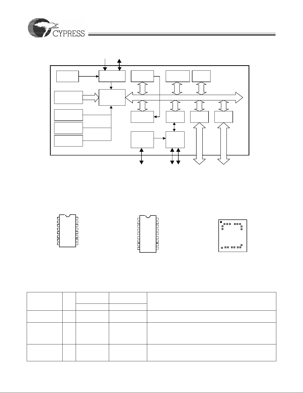
3.0 Logic Block Diagram
XTALIN/P2.1 XTALOUT/P2.2
XT ALIN/P2 .1 XT ALOUT
FOR
FOR
enCoRe™ USB
CY7C63221/31A
Internal
Oscillator
EPROM
3 Kbytes
Brown-Out
Reset
Watch Dog
Timer
Low Voltage
Reset
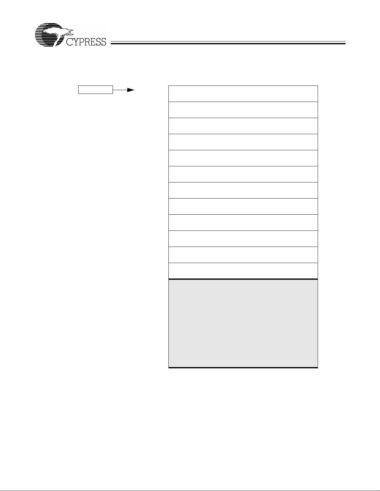
4.0 Pin Configurations
CY7C63221A
16-pin PDIP
P0.0
P0.1
P0.2
P0.3
V
SS
V
PP
VREG/P2.0
XTALIN/P2.1
1
2
3
4
5
6
7
8
P0.4
16
15
P0.5
P0.6
14
P0.7
13
12
D+/SCLK
11
D–/SDATA
10
V
XTALOUT/P2.2
9
CC
Xtal
Os cillator
8-bit
RISC
Core
Wake-Up
Timer
Interru p t
Controller
3.3V
Regulator
RAM
96 Bytes
USB
Engine
USB &
PS/2
Xcvr
12-bit
Timer
Port 0
GPIO
VREG/P2.0 D+ D- P0.0-P0.7 P1.0-P1.1
(Top View)
CY7C63231A
18-pin SOIC/PDIP
P0.0
1
P0.1
2
P0.2
3
P0.3
4
P1.0
5
6
V
SS
7
V
PP
VREG/P2.0
XTALIN/P2.1
8
9
P0.4
18
17
P0.5
P0.6
16
P0.7
15
P1.1
14
13
D+/SCLK
12
D–/SDATA
11
V
XTALOUT/P2.2
10
CC
CY7C63221A-XC
DIE
P0.3
P1.0
Vss
Port 1
GPIO
4
5
6
3 P0.2
2 P0.1
7 8 9
Vpp
VREG/P2.0
1 P0.0
18 P0.4
101112
XTALIN/P2.1
XTALOUT/P2.2
17 P0.5
Vcc
16 P0.6
15
14
13
D-/SDATA
P0.7
P1.1
D+/SCLK
5.0 Pin Assignments
CY7C63221A
Name I/O
D–/SDAT A,
D+/SCLK
I/O 11
12
P0[7:0] I/O 1, 2, 3, 4,
13, 14, 15, 16
P1[1:0] I/O NA 5,14 IO Port 1 capabl e of sinking up to 50 mA/pin, o r sinking control led
Document #: 38-08028 Rev. *A Page 7 of 49
CY7C63231/
CY7C63221-XC
12
13
1, 2, 3, 4,
15, 16, 17, 18
Description16-Pin 18-Pin/Pad
USB differential data lines (D– and D+), or PS/2 clock and data
signals (SDATA and SCLK)
GPIO Port 0 capable of sinking up to 50 mA/pin, or sinking
controlled low or high programmable current. Can also source
2 mA current, provide a resistive pull-up, or serve as a highimpedance input.
low or high program mable current. Can also source 2 m A current,
provide a resistive pull-up, or serve as a high-impedance input.

FOR
FOR
enCoRe™ USB
CY7C63221/31A
5.0 Pin Assignments (continued)
CY7C63221A
Name I/O
XTALIN/P2.1 IN 8 9 6-MHz ceramic resonator or external clock input, or P2.1 input
XTALOUT/P2.2 IN 9 10 6-MHz ceramic resonator return pin or internal oscillator output,
V
PP
V
CC
VREG/P2.0 7 8 Voltage supply for 1.3-kΩ USB pull-up resistor (3.3V nominal).
V
SS
6 7 Programming voltage supply, ground for normal operation
10 1 1 Volt age supply
5 6 Ground
6.0 Programming Model
Refer to the CYASM Assembler User’s Guide for more details on firmware operation with the CY7C632XX microcontrollers.
6.1 Program Counter (PC)
The 14-bit program coun ter (PC) allows access f or 3 Kbytes of EPROM usi ng the CY7C632XX arc hitecture. The prog ram counter
is cleared during rese t, such that the first instruct ion executed after a reset is at address 0x0000. This is typically a jump instruction
to a reset handler that initializes the application.
The lower 8 bits of the program counter are incre mented as instructi ons are loaded and exec uted. The upper 6 bit s of the program
counter are incremented by executing an XPAGE instruction. As a result, the last instruction executed within a 256-byte “page”
of sequential code should be an XPAGE instruction. The assembler directive “XPAGEON” will cause the assembler to insert
XPAGE instructions automatically. As instructions can be either one or two bytes long, the assembler may occasionally need to
insert a NOP followed by an XPAGE for correct execution.
The program counter of the next in struction to be ex ecuted, carry flag, and zero flag are saved as two by tes on the program st ack
during an interrupt acknowledge or a CALL instruction. The program counter, carry flag, and zero flag are restored from the
program stack only during a RETI instruction.
Please note the program counter cannot be accessed directly by the firmware. The program stack can be examined by reading
SRAM from location 0x00 and up.
Note that there are rest rictions in using t he JMP , CALL, and INDEX instructi ons across the 4-KB boun dary of the program memo ry .
Refer to the CYASM Assembler User’s Guide for a detailed description.
CY7C63231/
CY7C63221-XC
Description16-Pin 18-Pin/Pad
or P2.2 input
Also serves as P2.0 input.
6.2 8-bit Accumulator (A)
The accumulator is the general-purpose, do-everything register in the architecture where results are usually calculated.
6.3 8-bit Index Register (X)
The index register “X” is available to the firmware a s an auxiliary accumulator. The X register also allow s the processo r to perform
indexed operations by loading an index value into X.
6.4 8-bit Program Stack Pointer (PSP)
During a reset, the program sta ck poin ter (PSP) i s set to ze ro. Th is means the pro gra m “stack” starts at R AM addre ss 0x 00 an d
“grows” upward from there. Note that the program stack pointer is directly addressable under firmware control, using the MOV
PSP,A instruction. The PSP supports interrupt service under hardware control and CALL, RET, and RETI instructions under
firmware control.
During an interrupt acknowledge, interrupts are disabled and the program counter, carry flag, and zero flag are written as two
bytes of data memory. The first byte is stored in the memory addressed by the program stack pointer, then the PSP is incremented.
The second byte is store d i n m em ory add res sed by th e pro gra m s t ac k poi nter and the PSP is incremented ag ain . Th e ne t effect
is to store the program counter and flags on the program “stack” and increment the program stack pointer by two.
The return from interrupt (RETI) instruction decrements the program stack pointer, then restores the second byte from memory
addressed by the PSP. The program stack pointer is decremented again and the first byte is restored from memory addressed
by the PSP. After the program counter and flags have be en restored from stack, the interrupts are enab led. The effect is to restore
the program counter and flags from the program stack, decrement the program stack pointer by two, and re-enable interrupts.
Document #: 38-08028 Rev. *A Page 8 of 49

FOR
FOR
enCoRe™ USB
CY7C63221/31A
The call subrou tine (CALL) instru ction stores the program co unter and flags o n the program s tack and increments th e PSP by two.
The return from subroutin e (RET) instructio n restores the p rogram cou nter , but not the flags, from pro gram stack a nd decrement s
the PSP by two.
6.5 8-bit Data Stack Pointer (DSP)
The data stack pointer (DSP) supports PUSH and POP instructions that use the data stack for temporary storage. A PUSH
instruction will pre-decrem ent the DSP, then wr ite dat a to the memory location addresse d by the D SP. A POP instruction will rea d
data from the memory location addressed by the DSP, then post-increment the DSP.
During a reset, the Data Stack Pointer will be set to zero. A PUSH instruction when DSP equals zero will write data at the top of
the data RAM (address 0xFF). This would write data to the memory area reserved for a FIFO for USB endpoint 0. In non-USB
applications, this works fine and is not a problem.
For USB applications , the firmw are shou ld set the DSP to a n appropriate location to avoid a memo ry confli ct with RAM dedic ated
to USB FIFOs. Since there are only 80 bytes of RAM available (except Endpoint FIFOs) the DSP should be set between 0x00
and 0x4Fh. The memory requirements for the USB endpoints are shown in Section 8.2. For example, assembly instructions to
set the DSP to 20h (giving 32 bytes for pr ogram and da ta stack combined) are shown bel ow:
MOV A,20h ; Move 20 hex into Accumulator (must be D8h or less to avoid USB FIFOs)
SWAP A,DSP ; swap accumulator value into DSP register
6.6 Address Modes
The CY7C632XX microcontroller supports three addressing modes for instructions that require data operands: data, direct, and
indexed.
6.6.1 Data
The “Data” address mode refers to a da ta ope rand that is actua lly a cons tant encoded in the i nstruction . As an example , consid er
the instruction that loads A with the constant 0x30:
• MOV A, 30h
This instruction will require two bytes of code where the first byte identifies the “MOV A” instruction with a data operand as the
second byte. The second byte of the instruction will be the constant “0xE8h”. A constant may be referred to by name if a prior
“EQU” statement assigns the constant value to the name. For example, the following code is equivalent to the example shown
above:
• DSPINIT: EQU 30h
• MOV A,DSPINIT
6.6.2 Direct
“Direct” address mode is used when the data operand is a variable stored in SRAM. In that case, the one byte address of the
variable is encoded in the instruction. As an example, consider an instruction that loads A with the contents of memory address
location 0x10h:
• MOV A, [10h]
In normal usage, variable names are assigned to variable addresses using “EQU” statements to improve the readability of the
assembler source code. As an example, the following code is equivalent to the example shown above:
• buttons: EQU 10h
• MOV A,[buttons]
6.6.3 Indexed
“Indexed” address mode allows the firmware to manipulate arrays of data stored in SRAM. The address of the data operand is
the sum of a constant encoded in the instruction and the contents of the “X” register. In normal usage, the constant will be the
“base” address of an array of data and the X register will contain an index that indicates which element of the array is actually
addressed:
• array: EQU 10h
• MOV X,3
• MOV A,[x+array]
This would have the effect of loading A with the fourth element of the SRAM “array” that begins at address 0x10h. The fourth
element would be at address 0x13h.
Document #: 38-08028 Rev. *A Page 9 of 49

FOR
FOR
enCoRe™ USB
CY7C63221/31A
7.0 Instruction Set Summary
Refer to the CY ASM Assembler User’s Guide for detaile d information on thes e instructions. Note that conditional jump instructions
(i.e. JC, JNC, JZ, JNZ) take 5 cycles if jump is taken, 4 cycles if no jump.
MNEMONIC Operand Opcode Cycles
HALT 00 7
ADD A,expr data 01 4
ADD A,[expr] direct 02 6
ADD A,[X+expr] index 03 7
ADC A,expr data 04 4
ADC A,[expr] direct 05 6
ADC A,[X+expr] index 06 7
SUB A,expr data 07 4
SUB A,[expr] direct 08 6
SUB A,[X+expr] index 09 7
SBB A,expr data 0A 4
SBB A,[expr] direct 0B 6
SBB A,[X+expr] index 0C 7
OR A,expr data 0D 4
OR A,[expr] direct 0E 6
OR A,[X+expr] index 0F 7
AND A,expr data 10 4
AND A,[expr] direct 11 6
AND A,[X+expr] index 12 7
XOR A,expr data 13 4
XOR A,[expr] direct 14 6
XOR A,[X+expr] index 15 7
CMP A,expr data 16 5
CMP A,[expr] direct 17 7
CMP A,[X+expr] index 18 8
MOV A,expr data 19 4
MOV A,[expr] direct 1A 5
MOV A,[X+expr] index 1B 6
MOV X,expr data 1C 4
MOV X,[expr] direct 1D 5
reserved 1E
XPAGE 1F 4
MOV A,X 40 4
MOV X,A 41 4
MOV PSP,A 60 4
CALL addr 50 - 5F 10
JMP addr 80-8F 5
CALL addr 90-9F 10
JZ addr A0-AF 5 (or 4)
JNZ addr B0-BF 5 (or 4)
MNEMONIC Operand Opcode Cycles
NOP 20 4
INC A acc 21 4
INC X x 22 4
INC [expr] direct 23 7
INC [X+expr] index 24 8
DEC A acc 25 4
DEC X x 26 4
DEC [expr] direct 27 7
DEC [X+ex p r ] ind ex 28 8
IORD expr address 29 5
IOWR expr address 2A 5
POP A 2B 4
POP X 2C 4
PUSH A 2D 5
PUSH X 2E 5
SWAP A,X 2F 5
SWAP A,DSP 30 5
MOV [expr],A direct 31 5
MOV [X+expr],A index 32 6
OR [expr],A direct 33 7
OR [X+exp r],A index 34 8
AND [expr],A direct 35 7
AND [X+expr],A index 36 8
XOR [expr],A direct 37 7
XOR [X+expr],A index 38 8
IOWX [X+expr] index 39 6
CPL 3A 4
ASL 3B 4
ASR 3C 4
RLC 3D 4
RRC 3E 4
RET 3F 8
DI 70 4
EI 72 4
RETI 73 8
JC addr C0-CF 5 (or 4)
JNC addr D0-DF 5 (or 4)
JACC addr E0-EF 7
INDEX addr F0-FF 14
Document #: 38-08028 Rev. *A Page 10 of 49
FOR
FOR
8.0 Memory Organization
8.1 Program Memory Organization
After reset Address
14-bit PC 0x0000 Program execution begins here after a reset.
enCoRe™ USB
CY7C63221/31A
0x0002 USB Bus Reset interrupt vector
0x0004 128-µs timer interrupt vector
0x0006 1.024-ms timer interrupt vector
0x0008 USB endpoint 0 interrupt vector
0x000A USB endpoi nt 1 interrupt vector
0x000C Reserved
0x000E Reserved
0x0010 Reserved
0x0012 Reserved
0x0014 GPIO interrupt vector
0x0016 Wake-up interrupt vector
0x0018 Program Memory begins here
0x0BDF 3 KB PROM ends here (3K - 32 bytes). See Note 1 belo w
Figure 8-1. Program Memory Space with Interrupt Vector Table
Note:
1. The upper 32 bytes of the 3K PROM are reserved. Therefore, user’s program must not over-write this space.
Document #: 38-08028 Rev. *A P age 11 of 49
FOR
FOR
enCoRe™ USB
CY7C63221/31A
8.2 Data Memory Organization
The CY7C632XX microcontroller provides 96 bytes of data RAM. In normal usage, the SRAM is partitioned into four areas:
program stack, data stack, user variables and USB endpoint FIFOs as shown below:
After reset Address
8-bit DSP 8-bit PSP 0x00 Progr am S tack Growth
(User’s firmware
moves DSP)
8-bit DSP User selected Data St ack Growth
User Variables
0x4F
0xF0
0xF8
Top of RAM Memory 0xFF
USB FIFO for Address A endpoint 1
USB FIFO for Address A endpoint 0
Document #: 38-08028 Rev. *A Page 12 of 49

FOR
FOR
enCoRe™ USB
CY7C63221/31A
8.3 I/O Register Summary
I/O registers are accessed via the I/O Read (IO RD) and I/O W ri te (IOWR, IOW X) instru ction s. IORD reads the selecte d port into
the accumulator. IOWR writes data from the accumulator to the selected port. Indexed I/O Write (IOWX) adds the contents of X
to the address in the instruction to form the port address and writes data from the accumulator to the specified port. Note that
specifying address 0 with IOWX (e.g., IOWX 0h) means the I/O port is selected solely by the contents of X.
Note: All bits of all registers are cleared to all zeros on reset, except the Processor Status and Control Register (Figure 18-
1). All registers not listed are reserved, and should never be written by firmware. All bits marked as reserved should always be
written as 0 and be treated as undefined by reads.
Table 8-1. I/O Register Summary
Register Name I/O Address Read/Write Function Fig.
Port 0 Data 0x00 R/W GPIO Port 0 12-2
Port 1 Data 0x01 R/W GPIO Port 1 12-3
Port 2 Data 0x02 R Auxiliary input register for D+, D–, VREG, XTALIN,
XTALOUT
Port 0 Interrupt Enable 0x04 W Interrupt enable for pins in Port 0 19-4
Port 1 Interrupt Enable 0x05 W Interrupt enable for pins in Port 1 19-5
Port 0 Interrupt Polarity 0x06 W Interrupt polarity for pins in Port 0 19-6
Port 1 Interrupt Polarity 0x07 W Interrupt polarity for pins in Port 1 19-7
Port 0 Mode0 0x0A W Controls output configuration for Port 0 12-4
Port 0 Mode1 0x0B W 12-5
Port 1 Mode0 0x0C W Controls output configuration for Port 1 12-6
Port 1 Mode1 0x0D W 12-7
USB Device Address 0x10 R/W USB Device Address register 14-1
EP0 Counter Register 0x11 R/W USB Endpoint 0 counter register 14-4
EP0 Mode Register 0x12 R/W USB Endpoint 0 configuration register 14-2
EP1 Counter Register 0x13 R/W USB Endpoint 1 counter register 14-4
EP1 Mode Register 0x14 R/W USB Endpoint 1 configuration register 14-3
USB Status & Control 0x1F R/W USB status and control register 13-1
Global Interrupt Enable 0x20 R/W Global interrupt enable register 19-1
Endpoint Interrupt Enable 0x21 R/W USB endpoint interrupt enables 19-2
Timer (LSB) 0x24 R Lower 8 bits of free-running timer (1 MHz) 17-1
Timer (MSB) 0x25 R Upper 4 bits of free-running timer 17-2
WDR Clear 0x26 W Watch Dog Reset clear -
Clock Configuration 0xF8 R/W Internal / External Clock configuration register 9-2
Processor Status & Control 0xFF R/W Processor status and control 18-1
12-8
Document #: 38-08028 Rev. *A Page 13 of 49
FOR
FOR
enCoRe™ USB
CY7C63221/31A
9.0 Clocking
The chip can be clocked from either the internal on-chip clock, or from an oscillator based on an external resonator/crystal, as
shown in Figure 9-1. No additional capacit ance is in clude d on c hip at the XTALIN/OUT pins. Operation is control led by the Cl ock
Configurat ion Register, Figure 9-2.
Internal Osc
Int Clk Output Disable
Port 2.2
XTALOUT
Ext Osc Enable
Clk2x (12 MHz)
(to Microcontroller)
Clock
Doubler
XTALIN
Clk1x (6 MHz)
(to USB SIE)
Port 2.1
Figure 9-1. Clock Oscillator On-chip Circuit
Bit # 76543210
Bit Name Ext. Clock
Resume
Delay
Wake-up Timer Adjust Bit [2:0] Low-voltage
Reset
Disable
Precision
USB
Clocking
Enable
Internal
Clock
Output
Disable
External
Oscillator
Enable
Read/Write R/W R/W R/W R/W R/W R/W R/W R/W
Reset 00000000
Figure 9-2. Clock Configuration Register (Address 0xF8)
Bit 7: Ext. Clock Resume Delay
External Clock Resume Delay bit selects the delay time when switching to the external oscillator from the internal oscillator
mode, or when waking from suspend mode with the external oscillator enabled.
1 = 4 ms delay.
0 = 128 µs delay.
The delay gives the oscillator time to start up. The shorter time is adequate for operation with ceramic resonators, while the
longer time is pre ferred for st art-up with a crystal . (These time s do not incl ude an initial oscillator start-up ti me which d epends
on the resonating element. This time is typically 50–100 µs for ceramic resonators and 1–10 ms for crystals). Note that this
bit only selects the del ay time for the extern al cloc k mode. When wak ing from suspend mo de with the interna l oscillat or (Bit 0
is LOW), the delay time is only 8 µs in addition to a delay of approximately 1 µs for the oscillator to start.
Bit [6:4]: Wake-up Timer Adjust Bit [2:0]
The Wake-up Timer Adjust Bits are used to adjust the Wake-up timer period.
If the Wak e-up interrupt is e nabled in the Global Inte rrupt Enable Regi ster , the mic rocontroller wi ll generate w ake-up interr upts
periodically. The frequency of these periodical wake-up interrupts is adjusted by setting the Wake-up Timer Adjust Bit [2:0],
as described in Section 11.2. One common use of the wake-up interrupts is to generate periodical wake-up events during
suspend mode to check for changes, such as looking for movement in a mouse, while maintaining a low average power.
Bit 3: Low-voltage Reset Disable
When V
microcontroller enters a partial suspend state for a period of t
drops below V
CC
(see Section 23.0 for the value of V
LVR
) and the Low-voltage Reset circuit is enabled, the
LVR
(see Sec tion 24.0 for th e value of t
START
START
). Program
Document #: 38-08028 Rev. *A Page 14 of 49

FOR
FOR
enCoRe™ USB
CY7C63221/31A
execution begins from address 0x0000 after this t
executes code. See Section 10.1 for more details.
delay period. This provides time for VCC to stabilize before the part
START
1 = Disables the LVR circuit.
0 = Enables t he LVR circuit.
Bit 2: Precision USB Clocking Enable
The Precision USB Clocking Enable only affects operation in internal oscillator mode. In that mode, this bit must be set to
1 to cause the internal cloc k to automatically p recisely tune to U SB timing requireme nts (6 MH z ± 1.5%). The freque ncy
may have a looser initial tolerance at power-up, but all USB transmissions from the chip will meet the USB specification.
1 = Enabled. The internal clock accuracy is 6 MHz ±1.5% after USB traffic is received.
0 = Disabled. The internal clock accuracy is 6 MHz ±5%.
Bit 1: Internal Clock Output Disable
The Internal Clock Out put Disable is used to keep the internal c lock from drivi ng out to the XTALOUT pin. This bit has no ef fect
in the external oscillator mode.
1 = Disable internal clock output. XTALOUT pin will drive HIGH.
0 = Enable the internal clock output. The internal clock is driven out to the XTALOUT pin.
Bit 0: External Oscillator Enable
At power-up, the chip operat es from th e interna l cloc k by def ault. Setti ng the Ext ernal Osc illato r Enab le bit HIG H disabl es the
internal clock, and halts the part while the external resonator/crystal oscillator is started. Clearing this bit has no immediate
effect, although the state of this bit is used when waking out of suspend mode to select between internal and external clock.
In internal clock mode, XTALIN pin will be configured as an input with a weak pull-down and can be used as a GPIO input
(P2.1).
1 = Enable the external oscillator. The clock is switched to external clock mode, as described in Section 9.1.
0 = Enable the internal oscillator.
9.1 Internal/External Oscillator Operati on
The internal oscillator provides an operating clock, factory set to a nominal frequency of 6 MHz. This clock requires no external
components. At p ow er-u p, the ch ip operates from the in ternal clock. In this m ode , th e i nte rnal c loc k is bu ffered and driven t o the
XTALOUT pin by default, and the state of the XTALIN pin can be read at Port 2.1. While the internal clock is enabled, its output
can be disabled at the XTALOUT pin by setting the Internal Clock Output Disable bit of the Clock Configuration Register.
Setting the External Oscillat or Enable bi t of the Clock Confi guratio n Registe r HIGH disab les the inter nal clo ck, and ha lts the part
while the external re sonat or/crys tal osci llator i s st arted . The step s in volv ed in sw itchin g from I nternal to Exter nal Cloc k mo de a re
as follows:
1. At reset, chip begins operation using the internal clock.
2. Firmware sets Bit 0 of the Clock Configuration Register. For example,
mov A, 1h ; Set Bit 0 HIGH (External Oscillator Enable bit). Bit 7 cleared gives faster start-up
iowr F8h ; Write to Clock Configuration Register
3. Internal clocking is halted, the internal oscillator is disabled, and the external clock oscillator is enabled.
4. After the external clock becomes stable , chip cloc ks are re-ena bled using the external clo ck signa l. (Note that the tim e for the
external clock to become stable depends on the external resonating device; see next section.)
5. After an additional delay the CPU is released to run. This delay depends on the state of the Ext. Clock Resume Delay bit of
the Clock Configuration Register. The time is 128 µs if the bit is 0, or 4 ms if the bit is 1.
6. Once the chip has been set to ex ternal oscillator , i t can only return to internal clock w hen waking from suspend mode . Clearing
bit 0 of the Clock Configuration Register will not re-enable internal clock mode until suspend mode is entered. See Section
11.0 for more details on suspend mode operation.
If the Internal Clock is enabled, the XTALIN pin can serve as a general-purpose input, and its state can be read at Port 2, Bit 1
(P2.1). Refer to Figure 12-8 for the Port 2 Data Register. In this mode, there is a weak pull-down at the XTALIN pin. This input
cannot provide an interrupt source to the CPU.
9.2 External Oscillator
The user can connect a low-cost ceramic resonator or an external oscillator to the XTALIN/XTALOUT pins to provide a precise
reference frequency for the chip clock, as shown in Figure 9-1. The e xterna l compone nts requir ed are a c eramic reso nator or
crystal and any associated capacitors. To run from the external resonator, the External Oscillator Enable bit of the Clock Configuration Register must be set to 1, as explained in the previous section.
Document #: 38-08028 Rev. *A Page 15 of 49

FOR
FOR
enCoRe™ USB
CY7C63221/31A
Start-up times for the external oscillator depend on the resonating device. Ceramic-resonator-based oscillators typically start in
less than 100 µs, whil e crys tal -based oscil lators tak e longe r, typically 1 to 10 ms. Board capac ita nce sh ould be minim ized on the
XTALIN and XTALOUT pins by keeping the traces as short as possible.
An external 6-MHz clock can be applied to the XTALIN pin if the XTALOUT pin is left open.
10.0 Reset
The USB Controller supports three types of resets. The effects of the reset are listed below. The reset types are:
1. Low-voltage Reset (LVR)
2. Brown-out Reset (BOR)
3. Watchdog Reset (WDR)
The occurrence of a re set is rec ord ed i n th e Pro ce ssor Status and Control Register (Figure 18-1). Bits 4 (Low-volt age or Bro w n-
out Reset bit) and 6 (Watchdog Reset bit) are used to record the occurrence of LVR/BOR and WDR respectively. The firmware
can interrogate these bits to determine the cause of a reset.
The microcontroller begins execution from ROM address 0x0000 after a LVR, BOR, or WDR reset. Although this looks like
interrupt vector 0, there is an important difference. Reset processing does NOT push the program counter, carry flag, and zero
flag onto program stack. Attempting to execute either a RET or RETI in the reset handler will cause unpredictable execution
results.
The following events take place on reset. More details on the various resets are given in the following sections.
1. All registers are reset to their default states (all bits cleared, except in Processor Status and Control Register).
2. GPIO and USB pins are set to high-impedance state.
3. The VREG pi n is set to high-impedance state.
4. Interrupts are disabled.
5. USB operation is disabled and must be enabled by firmware if desired, as explained in Section 14.1.
6. For a BOR or LVR , the external o scillator is disa bled and Internal Clock mode is ac tivated, followe d by a time-out p eriod t
to stabilize . A WDR does not chan ge the cloc k m ode, an d ther e is no del ay for VCC stabilizat ion on a WD R. No te tha t
for V
CC
the External Oscillator Enable (Bit 0, Figure 9-2) will be cleared by a WDR, but it does not take effect until suspend mode is
entered.
7. The Program Stack Pointer (PSP) and Data Stack Pointer (DSP) reset to address 0x00. Firmware should move the DSP for
USB applications, as explained in Section 6.5.
8. Program execution begins at address 0x0000 after the appropriate time-out period.
START
10.1 Low-voltage Reset (LVR)
When V
the point where V
of t
START
wait for V
As long as the LVR circuit is enabled, this reset sequ ence repea ts whene ver the V
be disabled by firmware by setting the Low-v oltage Res et Disable bit in the Clock Configu ration Register ( Figure 9-2). In addition,
the LVR is automatically disabled in suspend mode to save power. If the LVR was enabled before entering suspend mode, it
becomes active again once the suspend mode ends.
When L VR is disab led durin g normal operation (e.g., by writing ‘0’ t o the Low -volt age Reset Disab le bit in the Cloc k Configura tion
Register), the chip may enter an unknown state if V
normal operation . If L VR is disabled (e.g., by firmware or during suspe nd mode), a s econdary low-v oltage monito r , BOR, become s
active, as described in the next section. The LVR/BOR Reset bit of the Processor Status and Control Register (Figure 18-1), is
set to ‘1’ if either a LVR or BOR has occurred.
is first applied to the ch ip, the internal oscillator is s tarted and the Lo w-vol tage Reset is in iti all y ena ble d b y d efa ult. At
CC
(see Section 24.0 for the value of t
to stabilize before it begins executing code from address 0x0000.
CC
has risen above V
CC
(see Section 23.0 for the value o f V
LVR
). During this t
START
drops below V
CC
START
), an internal counter s tarts counting for a period
LVR
time, the microcontroller enters a partial suspend state to
pin voltage dr ops bel ow V
CC
. Therefore, LVR should be enabled at all times during
LVR
. The L VR can
LVR
10.2 Brown-out Reset (BOR)
The Brown-out Reset (BOR) circuit is always active and behaves like the POR. BOR is asserted whenever the V
the device is below an internally defined trip voltage of approximately 2.5V. The BOR re-enables LVR. That is, once V
and trips BOR, the part rem ains in reset until V
resumes, and the microcontroller starts executing code from address 0x00 after the t
In suspend mode, only the BOR detection is active, giving a reset if V
suspended and cod e is not e xecuting, th is lowe r reset vo ltage is safe f or retai ning the s tate o f all regis ters and memory. Note that
rises above V
CC
. At that point, the t
LVR
drops below approximately 2.5V. Since the device is
CC
delay occurs before norma l operation
START
delay.
START
in suspend mode, LVR is disabled as discussed in Section 10.1.
Document #: 38-08028 Rev. *A Page 16 of 49
voltage to
CC
CC
drops
FOR
FOR
enCoRe™ USB
CY7C63221/31A
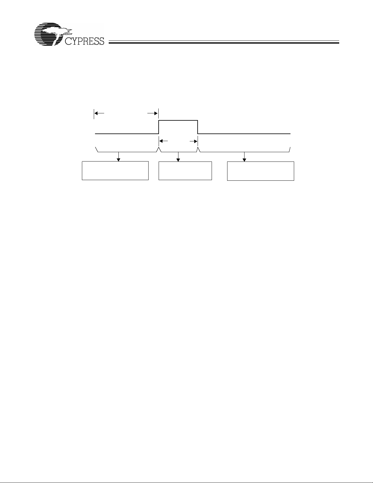
10.3 Watchdog Reset (WDR)
The Watchdog Timer Reset (WDR) occurs when the internal Watchdog timer rolls over. Writing any value to the write-only
Watchdog Rese t Re giste r at a ddr ess 0x26 will clear the t imer. The timer will roll o ver a nd WDR will occ ur if it i s no t cle ared within
(see Figure 10-1) of the last clear . Bit 6 (Watc hdog Reset bit) of th e Processor S t atus and Control Re gister is set to re cord
t
WATCH
this event (see Section 18.0 for mo re de t ai ls ). A Watchdog Timer Reset lasts for typ icall y 2 –4 ms af ter w hi ch the m ic roc ontr oll er
begins execution at ROM address 0x0000.
t
WATCH = 10.1 to
WDR
14.6 ms
(at F
OSC
= 6 MHz)
2–4 ms
At least 10.1 ms
since last write to WDR
WDR goes HIGH
for 2–4 ms
Execution begins at
ROM Address 0x0000
Figure 10-1. Watchdog Reset (WDR, Address 0x26)
11. 0 Suspend Mode
The CY7C632XX part s support a versatile low -power suspe nd mode. In suspe nd mode, only an enabled interru pt or a LOW st ate
on the D–/SDA TA pin will wake the part. T wo options are avail able. For lowes t power, all internal circuits can be disabled, so only
an external event will resume operation. Alternatively, a low-power internal wake-up timer can be used to trigger the wake-up
interrupt. This timer is described in Section 11.2, and can be used to periodically poll the system to check for changes, such as
looking for movement in a mouse, while maintaining a low average power.
The CY7C632XX is placed into a low-power state by setting the Suspend bit of the Processor Status and Control Register
(Figure 18-1). All logic blocks in the device are turned off except the GPIO interrupt logic, the D–/SDATA pin input receiver, and
(optionally) the wake-up timer. The clock oscillators, as well as the free-running and watchdog timers are shut down. Only the
occurrence of an enable d GP IO inte rrupt , w ake -up inte rrup t, SPI sl av e in terru pt, or a LO W st a te o n the D–/SDATA pin will wake
the part from suspend (D– LOW indicates non-idle USB activity). Once one of these resuming conditions occurs, clocks will be
restarted and the device returns to full operation after the oscillator is stable and the selected delay period expires. This delay
period is determined by s ele cti on of inte rna l vs . ex terna l cl oc k, a nd by the s t ate of the Ext. Clock Resume Delay as expl ai ned in
Section 9.0.
In suspend mode, any enabled and pending interrupt will wake the part up. The state of the Interrupt Enable Sense bit (Bit 2,
Figure 18-1) does not have any effect. As a result, any inte rrupts not inten ded for waking from suspend should be disabled throug h
the Global Interrupt Enable Register and the USB End Point Interrupt Enable Register (Section 19.0).
If a resuming condition exi sts when the suspend bi t is set, the part w ill stil l go into su spend and then awak e after the ap prop riate
delay time. The Run bit in the Processor Status and Control Register must be set for the part to resume out of suspend.
Once the clock i s sta ble and the delay time ha s expired , the mic rocontrol ler will execute th e instruc tion foll owing th e I/O wr ite that
placed the device into suspend mode before servicing any interrupt requests.
T o ac hieve the lowe st possible current during s uspend mode, al l I/O should b e held at either V
bit interrupts (Figure 19-4 and Figure 19-5) should be disabled for any pins that are no t bei ng us ed for a wake-up interrupt. This
should be done even if the main GPIO Interrupt Enable (Figure19-1) is off.
Typical code for entering suspend is shown below:
... ; All GPIO set to low-power state (no floating pins, and bit interrupts disabled unless using for wake-up)
... ; Enable GPIO and/or wake-up timer interrupts if desired for wake-up
... ; Select clock mode for wake-up (see Section 11.1)
mov a, 09h ; Set suspend and run bits
iowr FFh ; Write to Status and Control Register - Enter suspend, wait for GPIO/wake-up interrupt or USB activity
nop ; This executes before any ISR
... ; Remaining code for exiting suspend routine
or ground. In addition, the GPIO
CC
Document #: 38-08028 Rev. *A Page 17 of 49

FOR
FOR
enCoRe™ USB
CY7C63221/31A
11.1 Clocking Mode on Wake-up from Suspend
When exiting suspend on a wake-up event, the device can be configured to run in either Internal or External Clock mode. The
mode is selected by the state of the External Oscillator Enable bit in the Clock Configuration Register (Figure 9-2). Using the
Internal Clock saves the external oscillator start-up time and keeps that oscillator off for additional power savings. The external
oscillator mode can be activated when desired, similar to operation at power-up.
The sequence of events for these modes is as follows:
Wake in Internal Clock Mode:
1. Before entering suspend, clear bit 0 of the Clock Configuration Register. This selects Internal clock mode after suspend.
2. Enter suspend mode by setting the suspend bit of the Processor Status and Control Register.
3. After a wake-up event, the internal clock starts immediately (within 2 µs).
4. A time-out period of 8 µs passes, and then firmware execution begins.
5. At some later point, to activate External Cl ock mode, set bit 0 of the Clock Configura tion Register . This halts the intern al clocks
while the external clock becomes stable. After an additional time-out (128 µs or 4 ms, see Section 9.0), firmware execution
resumes.
Wake in External Clock Mode:
1. Before entering suspend, the extern al cl oc k m us t b e s ele cted by setting bit 0 of the Clock Configu rati on R egi ste r. Make sure
this bit is still set when suspend mode is entered. This selects External clock mode after suspend.
2. Enter suspend mode by setting the suspend bit of the Processor Status and Control Register.
3. After a wake-up event, the external oscillator is st a r ted . The clo ck is mo ni tore d for stability (this takes approximately 50 –100
µs with a ceramic resonator).
4. After an additional time-out period (128 µs or 4 ms, see Section 9.0), firmware execution resumes.
11.2 Wake-up Timer
The wake-up timer runs whenever the wake-up interrupt is enabled, and is turned off whenever that interrupt is disabled.
Operation is independent of whether the device is in suspend mode or if the global interrupt bit is enabled. Only the Wake-up
Timer Interrupt Enable bit (Figure 19-1) controls the wake-up timer.
Once this timer is a cti va ted , it will give interrupts after it s tim e-o ut period (see belo w) . Th ese interrupts conti nu e p eri odi cally u nti l
the interrupt is disabled. Whenever the interrupt is disabled, the wake-up timer is reset, so that a subsequent enable always
results in a full wake-up time.
The wake-up timer can be adjusted by the user through the Wake-up Timer Adjust bits in the Clock Configuration Register
(Figure 9-2). These bits cl ear on rese t. In addit ion to allow ing the u ser to selec t a range for the wa ke-up time , a firmware algorithm
can be used to tune out initial process and operating condition variations in this wake-up time. This can be done by timing the
wake-up interrupt time with the acc urate 1.024-m s timer interru pt, and adju sting the T i mer Adju st bits ac cordingly to approxi mate
the desired w ake-up time.
Table 11-1. Wake-up Timer Adjust Settings
Adjust Bits [2:0]
(Bits [6:4] in Figure 9-2) Wake-up Time
000 (reset state) 1 * t
001 2 * t
010 4 * t
011 8 * t
100 16 * t
101 32 * t
110 64 * t
111 128 * t
See Section 24.0 for the value of t
WAKE
WAKE
WAKE
WAKE
WAKE
WAKE
WAKE
WAKE
WAKE
Document #: 38-08028 Rev. *A Page 18 of 49

FOR
FOR
enCoRe™ USB
CY7C63221/31A
12.0 General Purpose I/O Ports
Ports 0 and 1 provide up to 10 versatile GPIO pins that can be read or written (the number of pins depends on package type).
V
GPIO
Mode
2
CC
Q3
GPIO
Internal
Data Bus
Data
Out
Register
Q1
Control
14 kΩ
Pin
Port Write
Interrupt
Polarity
Interrupt
Enable
Port Read
Interrupt
Logic
Threshold Select
Q2
To Interrupt
Controller
Figure 12-1. Block Diagram of GPIO Port (one pin shown)
Port 0 is an 8-bit port; Port 1 contains 2 bits, P1.1–P1.0 in the CY7C63231 and CY7C63221A-XC parts. Each bit can also be
selected as an interrupt source for the microcontroller.
The data for each GPIO pin is accessible through the Port Data Register. Writes to the Port Data Register store outgoing data
state for the port pins, while reads from the Port Data Register return the actual logic value on the port pins, not the Port Data
Register content s.
Each GPIO pin is configured independently. The driving state of each GPIO pin is determined by the value written to the pin’s
Data Register and by two associated pin’s Mode0 and Mode1 bits.
The Port 0 Data Register is shown in Figure 12-2, and the Port 1 Data R egi ste r is s how n in Figure 12-3. The Mode0 and M ode 1
bits for the two GPIO ports are given in Figure 12-4 through Figure 12-7.
Bit # 76543210
Bit Name P0
Read/Write R/W R/W R/W R/W R/W R/W R/W R/W
Reset 00000000
Figure 12-2. Port 0 Data (Address 0x00)
Bit [7:0]: P0[7:0]
1 = Port Pin is logic HIGH
0 = Port Pin is logic LOW
Document #: 38-08028 Rev. *A Page 19 of 49

FOR
FOR
enCoRe™ USB
CY7C63221/31A
Bit # 76543210
Bit Name Reserved P1[1:0]
Notes Pins 1:0 in all parts
Read/Write ------R/WR/W
Reset 00000000
Figure 12-3. Port 1 Data (Address 0x01)
Bit [7:2]: Reserved
Bit [1:0]: P1[1:0]
1 = Port Pin is logic HIGH
0 = Port Pin is logic LOW
Bit # 76543210
Bit Name P0[7:0] Mode0
Read/Write WWWWWWWW
Reset 00000000
Figure 12-4. GPIO Port 0 Mode0 Register (Address 0x0A)
Bit [7:0]: P0[7:0] Mode 0
1 = Port Pin Mo de 0 is logic HIGH
0 = Port Pin Mode 0 is logic LOW
Bit # 76543210
Bit Name P0[7:0] Mode1
Read/Write WWWWWWWW
Reset 00000000
Figure 12-5. GPIO Port 0 Mode1 Register (Address 0x0B)
Bit [7:0]: P0[7:0] Mode 1
1 = Port Pin Mo de 1 is logic HIGH
0 = Port Pin Mode 1 is logic LOW
Bit #76543210
Bit Name Reserved P1[1:0] Mode0
Read/Write ------WW
Reset 00000000
Figure 12-6. GPIO Port 1 Mode0 Register (Address 0x0C)
Bit [7:2]: Reserved
Bit [1:0]: P1[1:0] Mode 0
1 = Port Pin Mo de 0 is logic HIGH
0 = Port Pin Mode 0 is logic LOW
Document #: 38-08028 Rev. *A Page 20 of 49

FOR
FOR
enCoRe™ USB
CY7C63221/31A
Bit #76543210
Bit Name Reserved P1[1:0] Mode1
Read/Write ------WW
Reset 00000000
Figure 12-7. GPIO Port 1 Mode1 Register (Address 0x0D)
Bit [7:2]: Reserved
Bit [1:0]: P1[1:0] Mode 1
1 = Port Pin Mo de 1 is logic HIGH
0 = Port Pin Mode 1 is logic LOW
Each pin can be independently configured as high-impedance inputs, inputs with internal pull-ups, open drain outputs, or traditional CMOS outputs with selectable drive strengths.
The driving state of eac h GPIO pin i s determined by the value writt en to the pin’s Data Registe r and by it s assoc iated Mod e0 and
Mode1 bits. Table12-1 lists the configuration states based on these bits. The GPIO ports default on reset to all Data and Mode
Registers cleared, so the pins are all in a high-impedance state. The available GPIO output drive strength are:
• Hi-Z Mode (Mode1 = 0 and Mode0 = 0)
Q1, Q2, and Q3 (Figure 12-1) are OFF. The GPIO pin is not driven internally. Performing a read from the Port Data Register
return the actual logic value on the port pins.
• Low Sink Mode (Mode1 = 1, Mode0 = 0, and the pin’s Data Register = 0)
Q1 and Q3 are OFF. Q2 is ON. The GPIO pin is capable of sinking 2 mA of current.
• Medium Sink Mode (Mode1 = 0, Mode0 = 1, and the pin’s Data Register = 0)
Q1 and Q3 are OFF. Q2 is ON. The GPIO pin is capable of sinking 8 mA of current.
• High Sink Mode (Mode1 = 1, Mode0 = 1, and the pin’s Data Register = 0)
Q1 and Q3 are OFF. Q2 is ON. The GPIO pin is capable of sinking 50 mA of current.
• High Drive Mode (Mode1 = 0 or 1, Mode0 = 1, and the pin’s Data Register = 1)
Q1 and Q2 are OFF. Q3 is ON. The GPIO pin is capable of sourcing 2 mA of current.
• Resistive Mode (Mode1 = 1, Mode0 = 0, and the pin’s Data Register = 1)
Q2 and Q3 are OFF. Q1 is ON. The GPIO pin is pulled up with an internal 14-kΩ resistor.
Note that open drain mode can be achieved by fixing the Data and Mode1 Registers LOW, and switching the Mode0 register.
Input thresholds are CMOS, or TTL as shown in the table (See Section 23.0 for the input threshold voltage in TTL or CMOS
modes). Both input modes include hysteresis to minimize noise sensitivity. In suspend mode, if a pin is used for a wake-up
interrupt using an external R-C circuit, CMOS mode is preferred for lowest power.
Table 12-1. Ports 0 and 1 Output Control Truth Table
Data Register Mode1 Mode0 Output Drive Strength Input Threshold
0
1 Hi-Z TTL
0
1 High Drive CMOS
0
1ResistiveCMOS
0
1 High Drive CMOS
00
Medium (8 mA) Sink CMOS
01
10
11
Hi-Z CMOS
Low (2 mA) Sink CMOS
High (50 mA) Sink CMOS
12.1 Auxiliary Input Port
Port 2 serves as an auxiliary input port as shown in Figure 12-8. The Port 2 inputs all have TTL input thresholds.
Document #: 38-08028 Rev. *A Page 21 of 49

FOR
FOR
enCoRe™ USB
CY7C63221/31A
Bit #76543210
Bit Name Reserved D+ (SCLK)
State
Read/Write - -RR- RRR
Reset 00000000
Figure 12-8. Port 2 Data Register (Address 0x02)
Bit [7:6]: Reserved
Bit [5:4]: D+ (SCLK) and D- (SDATA) States
The state of the D+ and D– pins can be read at Port 2 Data Register. Performing a read from the port pins returns their logic
values.
1 = Port Pin is logic HIGH
0 = Port Pin is logic LOW
Bit 3: Reserved
D– (SDATA)
State
Reserved P2.2
(Internal
Clock Mode
Only)
P2.1
(Internal
Clock Mode
Only)
P2.0
VREG Pin
State
Bit 2: P2.2 (Internal Clock Mode Only)
In the Internal Clock mode, the XTALOUT pin can serve as a general purpose input, and its state can be read at Port 2, Bit 2
(P2.2). See Section 9.1 f or more details.
1 = Port Pin is logic HIGH
0 = Port Pin is logic LOW
Bit 1: P2.1 (Internal Clock Mode Only)
In the Internal Clock mode, the XTALIN pin can serve as a general purpose input, and its state can be read at Port 2, Bit 1
(P2.1). See Section 9.1 f or more details.
1 = Port Pin is logic HIGH
0 = Port Pin is logic LOW
Bit 0: P2.0/ VREG Pin State
In PS/2 mode, the VREG
pin can be used as an input and its state can be read at port P2.0. Section 15.0 for more details.
1 = Port Pin is logic HIGH
0 = Port Pin is logic LOW
13.0 USB Serial Interface Engine (SIE)
The SIE allows the microcontroller to communicate with the USB host. The SIE simplifies the interface between the microcontroller and USB by incorporating hardware that handles the following USB bus activity independently of the microcontroller:
• Translate the encoded received data and format the data to be transmitted on the bus.
• CRC checking and generation. Flag the microcontroller if errors exist during transmission.
• Address checking. Ignore the transactions not addressed to the device.
• Send appropriate ACK/NAK/STALL handshakes.
• Token type identification (SETUP, IN, or OUT). Set the appropriate token bit once a valid token is received.
• Place valid received data in the appropriate endpoint FIFOs.
• Send and update the data toggle bit (Data1/0).
• Bit stuffing/unstuffing.
Firmware is required to handle the rest of the USB interface with the following tasks:
• Coordinate enumeration by decoding USB device requests.
• Fill and empty the FIFOs.
• Suspend/Resume coordination.
• Verify and select Data toggle values.
Document #: 38-08028 Rev. *A Page 22 of 49

FOR
FOR
enCoRe™ USB
CY7C63221/31A
13.1 USB Enumeration
A typical USB enumeration sequence is shown below. In this description, ‘Firmware’ refers to embedded firmware in the
CY7C632XX controller.
1. The host computer sends a SETUP packet followed by a DATA packet to USB address 0 requesting the Device descriptor.
2. Firmware decodes the request and retrieves its Device descriptor from the program memory tables.
3. The host computer performs a control read seq uence and Firmwa re responds by s ending the Device de scriptor over the USB
bus, via the on-chip FIFO.
4. After receiving the descriptor, the host sends a SETUP packet followed by a DATA packet to address 0 assigning a new USB
address to the device.
5. Firmware stores the new address in its USB Device Address Register after the no-data control sequence completes.
6. The host sends a request for the Device descriptor using the new USB address.
7. Firmware decodes the request and retrieves the Device descriptor from program memory tables.
8. The host performs a control read sequence and Firmware responds by sending its Device descriptor over the USB bus.
9. The host generates control reads from the device to request the Configuration and Report descriptors.
10.Once the device receives a Set Configuration request, its functions may now be used.
11.Firmware should take appropriate action for Endpoint 1 transactions, which may occur from this point.
13.2 USB Port Status and Control
USB status and control is regulated by the USB Status and Control Register as shown in Figure 13-1.
Bit # 76543210
Bit Name PS/2 Pull-up
Enable
Read/Write R/W R/W R/W - R/W R/W R/W R/W
Reset 00000000
Bit 7: PS/2 Pull-up Enable
This bit is used to enable the internal PS/2 pull-up resistors on the SDATA and SCLK pins. Normally the output high level on
these pins is V
or if the Device Address is enabled (bit 7 of the USB Device Address Register, Figure 14-1).
, but note that the output will be cl am pe d to app rox im atel y 1 Volt above V
CC
1 = Enable PS/2 pull-up res istors. The SDA T A and SCLK pi ns are pulled up interna lly to V
5kΩ (see Section 23.0 for the value of R
0 = Disable PS/2 pull-up resistors.
Bit 6: VREG Enable
A 3.3V voltage regulato r is integrated on chi p to provide a vol tage so urce for a 1.5-kΩ pull-u p resistor conne cted to the D– pi n
as required by the USB Specif ication. N ote that the VREG o utput has an inter nal series resistanc e of app roximate ly 200Ω, the
external pull-up resistor required is approximately 1.3-kΩ (see Figure 16-1).
1 = Enable the 3.3V output voltage on the VREG pin.
0 = Disable. The VREG pin can be configured as an input.
VREG
Enable
USB Reset-
PS/2 Activity
Reserved USB
Bus Activity
Interrupt
Mode
Figure 13-1. USB Status and Control Register (Address 0x1F)
REG
with two resistors of a pproximately
PS2
).
CC
D+/D- Forcing Bit
if the VREG Enable bit is set,
Bit 5: USB-PS/2 Interrupt Select
This bit allows the user to select whether an USB bus reset interrupt or a PS/2 activity interrupt will be generated when the
interrupt conditio ns are det ect ed.
1 = PS/2 interrupt mode. A PS/2 activity interrupt will occur if the SDATA pin is continuously LOW for 128 to 256 µs.
0 = USB interrupt mode (default state). In this mode, a USB bus reset interrupt will occur if the single ended zero (SE0, D–
and D+ are LOW) exists for 128 to 256 µs.
See Section 19.0 for more details.
Bit 4: Reserved. Must be written as a ‘0’.
Document #: 38-08028 Rev. *A Page 23 of 49

FOR
FOR
enCoRe™ USB
CY7C63221/31A
Bit 3: USB Bus Activity
The Bus Activity bit is a “sticky” bit that detects any non-idle USB event has occurred on the USB bus. Once set to HIGH by
the SIE to indicate the bus activity, this bit retains its logical HIGH value until firmware clears it. Writing a ‘0’ to this bit clears
it; writing a ‘1’ preserves its value. The user firmware should check and clear this bit periodically to detect any loss of bus
activity. Firmware can clear the Bus Activity bit, but only the SIE can set it. The 1.024-ms timer interrupt service routine is
normally used to check and clear the Bus Activity bit.
1 = There has been bus activity since the last time this bit was cleared. This bit is set by the SIE.
0 = No bus activity since last time this bit was cleared (by firmware).
Bit [2:0]: D+/D– Forcing Bit [2:0]
Forcing bits allow firmware to directly drive the D+ and D– pins, as shown in Table 13-1. Outputs are driven with controlled
edge rates in these modes for low EMI . For forcing the D+ and D– pins in USB mode, D+/D– Forcing Bit 2 should be 0. Setting
D+/D– Forcing Bit 2 to ‘1’ puts both pins in an open-drain mode, preferred for applications such as PS/2 or LED driving.
Table 13-1. Control Modes to Force D+/D– Outputs
D+/D– Forcing Bit [2:0] Control Action Application
000 Not forcing (SIE controls driver) Any Mode
001 Force K (D+ HIGH, D– LOW) USB Mode
010 Force J (D+ LOW, D– HIGH)
011 Force SE0 (D– LOW, D+ LOW)
100 Force D– LOW, D+ LOW PS/2 Mode
101 Force D– LOW, D+ HiZ
110 Force D– HiZ, D+ LOW
111 Force D– HiZ, D+ HiZ
Note:
2. For PS/2 operation, the D+/D- Forcing Bit [2:0] = 111b mode must be set initially (one time only) before using the other PS/2 force modes.
[2]
Document #: 38-08028 Rev. *A Page 24 of 49

FOR
FOR
enCoRe™ USB
CY7C63221/31A
14.0 USB Device
The CY7C632XX supports one USB Device Address with two endpoints: EP0 and EP1.
14.1 USB Address Register
The USB Device Address Register contains a 7-bit USB address and one bit to enable USB communication. This register is
cleared during a reset, setting the USB device address to zero and marking this address as disabled. Figure14-1 shows the
format of the USB Address Register.
Bit # 76543210
Bit Name Device
Address
Enable
Read/Write R/W R/W R/W R/W R/W R/W R/W R/W
Reset 00000000
Figure 14-1. USB Device Address Register (Address 0x10)
In either USB or PS/2 mode, this register is cleared by both hardware resets and the USB bus reset. See Section 19.3 for more
information on the USB Bus Reset - PS/2 interrupt.
Device Address Bit
Bit 7: Device Address Enable
This bit must be enabled by firm ware before the serial interfa ce engine (SIE) will respond to USB traf fic at the address specif ied
in Bit [6:0].
1 = Enable USB device address.
0 = Disable USB device address.
Bit [6:0]: Device Address Bit[6:0]
These bits must be set by firmw are during the USB enumera tion process (i.e., SetAddres s) to the non-zero add ress assigne d
by the USB host.
14.2 USB Control Endpoint
All USB devices are required to have an endpoint number 0 (EP0) that is used to initialize and control the USB device. EP0
provides access to the device configu ration informatio n and allows generi c USB status and control access es. EP0 is bidirectio nal,
as the device can both receive and transmit data. EP0 uses an 8-byte FIFO at SRAM locations 0xF8-0xFF, as shown in
Section 8.2.
The EP0 endpoint mode register uses the format shown in Figure14-2.
Bit # 76543210
Bit Name SETUP
Received
Read/Write R/W R/W R/W R/W R/W R/W R/W R/W
Reset 00000000
IN
Received
Figure 14-2. Endpoint 0 Mode Register (Address 0x12)
OUT
Received
ACKed
Transaction
Mode Bit
The SIE provides a lo cking feature to prevent firm w are from overw ri tin g bits in the USB Endpoint 0 Mode Register. Writes to the
register have no effect from the point that Bit[6:0] of the register are updated (by the SIE) until the firmware reads this register.
The CPU can unlock this register by reading it.
Because of these hardware-locking features, firmware should perform an read after a write to the USB Endpoint 0 Mode Register
and USB Endpoint 0 Count Regis ter (Figure 14-4) to verify that the content s ha ve cha nge d as des ire d, an d tha t the SIE has not
updated th ese values.
Bit [7:4] of this register are cleared by any non-locked write to this register, regardless of the value written.
Bit 7: SETUP Received
1 = A valid SETUP packet has been received. This bit is forced HIGH from the start of the data packet phase of the SETUP
transaction until the st art of the ACK packet retu rned by the SIE. The CPU is prevent ed from clearing this bit duri ng this interval.
Document #: 38-08028 Rev. *A Page 25 of 49

FOR
FOR
enCoRe™ USB
CY7C63221/31A
While this bit is set to ‘1’, the CPU cannot write to the EP0 FIFO. Th is prevent s firmw are from overwr iting an incom ing SETUP
transaction before firmware has a chance to read the SETUP data.
0 = No SETUP received. This bit is cleared by any non-locked writes to the register.
Bit 6: IN Received
1 = A valid IN packet has been received. This bit is updated to ‘1’ after the last received packet in an IN transaction. This bit
is cleared by any non-locked writes to the register.
0 = No IN received. This bit is cleared by any non-locked writes to the register.
Bit 5: OUT Received
1 = A valid OUT pac ket has been re ceiv ed. This bit is updated to ‘1’ after th e la st rece ived p ac ket in a n OUT tran sacti on. Thi s
bit is cleared by any non-locked writes to the register.
0 = No OUT received. This bit is cleared by any non-locked writes to the register.
Bit 4: ACKed Transaction
The ACKed T ran sacti on bit is s et whe never the SIE eng ages in a transa ction to th e regis ter's endp oint that comp letes wit h an
ACK packet.
1 = The transaction completes with an ACK
0 = The transaction does not complete with an ACK
Bit [3:0]: Mode Bit[3:0]
The endpoint modes determine how the SIE responds to USB traffic that the host sends to the endpoint. For example, if the
endpoint Mode Bits [3:0] are set to 0001 which is NAK IN/OUT mode as shown in Table 20-1, the SIE will send NAK handshakes in response to any IN or OUT token sent to this endpoint. In this NAK IN/OUT mode, the SIE will send an ACK
handshake when the host sends a SETUP token to this endpoint. The mode encoding is shown in Table 20-1. Additional
information on th e m od e b it s c an be found in Table 20-2 and Table 20-3. These modes give the fi rmware total control o n h ow
to respond to different tokens sent to the endpoints from the host.
In addition, the Mode Bits are automatically changed by the SIE in response to many USB transactions. For example, if the
Mode Bit [3:0] are set to 1011 which is ACK OUT-NAK IN mode as shown in Table 20-1, the SIE will change the endpoint
Mode Bit [3:0] to NAK IN/OUT (0001) mode after issuing an ACK handshake in response to an OUT token. Firmware needs
to update the mode for the SIE to respond appropriately.
14.3 USB Non-Control Endpoints
The CY7C632XX feature one non-control endpoint, endpoint 1 (EP1). The EP1 Mode Register does not have the locking
mechanism of the EP0 Mod e Re gister. The EP1 Mode Register uses t he form at sho wn in Figure14-3. EP1 uses an 8-byte FIFO
at SRAM locations 0xF0–0xF7 as shown in Section 8.2.
Bit # 76543210
Bit Name STALL Reserved ACKed
Transaction
Read/Write R/W - - R/C R/W R/W R/W R/W
Reset 00000000
Figure 14-3. USB Endpoint EP1 Mode Registers (Address 0x14)
Bit 7: STALL
1 = The SIE will stall an OUT packet if the Mode Bits are set to ACK-OUT, and the SIE will stall an IN packet if the mode bits
are set to ACK-IN. See Section 20.0 for the available modes.
0 = This bit must be set to LOW for all other modes.
Mode Bit
Bit [6:5]: Reserved. Must be written to zero during register writes.
Bit 4: ACKed Transaction
The ACKed transaction bit is set whene ver the SIE engag es in a transa ction to the register's end point tha t completes with an
ACK packet.
1 = The transaction completes with an ACK.
0 = The transaction does not complete with an ACK.
Document #: 38-08028 Rev. *A Page 26 of 49

FOR
FOR
enCoRe™ USB
CY7C63221/31A
Bit [3:0]: Mode Bit [3:0]
The EP1 Mode Bits operate in the same manner as the EP0 Mode Bits (see Section 14.2).
14.4 USB Endpoint Counter Registers
There are two Endpoint Counter registers, with identical formats for both control and non-control endpoints. These registers
contain byte coun t informati on for USB transa ctions, as well as bit s for dat a pack et statu s. The forma t of these reg isters is shown
in Figure 14-4.
Bit # 76543210
Bit Name Data Toggle Data Valid Reserve d Byte Count
Read/Write R/W R/W - - R/W R/W R/W R/W
Reset 00000000
Figure 14-4. Endpoint 0 and 1 Counter Registers (Addresses 0x11 and 0x13)
Bit 7: Data Toggle
This bit selects the DATA packet’s toggle state. For IN transactions, firmware must set this bit to the select the transmitted
Data Toggle. For OUT or SETUP transactions, the hardware sets this bit to the state of the received Data Toggle bit.
1 = DATA1
0 = DATA0
Bit 6: Data Valid
This bit is used for OUT and SETUP tokens only. This bit is cleared to ‘0’ if CRC, bitstuff, or PID errors have occurred. This
bit does not update for some endpoint mode settings. Refer to Table 20-3 for more details.
1 = Data is valid.
0 = Data is invalid. If enabled, the endpoint interrupt will occur even if invalid data is received.
Bit [5:4]: Reserved
Bit [3:0]: Byte Count Bit [3:0]
Byte Count Bits indicate the number of data bytes in a transaction: For IN transactions, firmware loads the count with the
number of bytes to be transmitted to the host from the endpoint FIFO. Valid values are 0 to 8 inclusive. For OUT or SETUP
transactions, the count is updated by hardware to the number of data bytes received, plus 2 fo r the CRC bytes. Valid values
are 2 to 10 inclusive.
For Endpoint 0 Count Register, whenever the count updates from a SETUP or OUT transaction, the count register locks and
cannot be written by the CPU. Reading the register unlocks it. This prevents firmware from overwriting a status update on
incoming SETUP or OUT transactions before firmware has a chance to read the data.
15.0 USB Regulator Output
The VREG pin provides a regulated output for connecting the pull-up resistor required for USB operation. For USB, a 1.5-kΩ
resistor is connected between the D– pin and the VREG voltage, to indicate low-speed USB operation. Since the VREG output
has an internal series resistance of approximately 200Ω, the external pull-up resistor required is R
The regulator output is pl aced i n a hig h-imp edance st ate at re set, a nd must b e enab led by firmware by se tting t he VREG En able
bit in the USB S t at us and C ontrol Registe r (Figure 13-1). This simplifies th e des ign of a comb inatio n PS/2-U SB devi ce, si nce th e
USB pull-up resistor can b e lef t in pl ac e duri ng PS/2 ope rati on wit hout loading the PS/2 line. In this mo de, the VR EG
used as an input and its state can be read at port P2.0. Refer to Figure 12-8 for the Port 2 data register. This input has a TTL
threshold.
In suspend mode, the regulator is automatically disabled. If VREG Enable bit is set (Figure 13-1), the VREG pin is pulled up to
with an internal 6.2-kΩ resis tor. This holds the proper VOH state in suspend mode.
V
CC
Note that enabling the device for USB (by setting the Device Address Enable bit, Figure 14-1) activates the internal regulator,
even if the VREG Enable bit is cleared to 0. This insures proper USB signaling in the case where the VREG pin is used as an
input, and an external regulator is provided for the USB pull-up resistor. This also limits the swing on the D– and D+ pins to about
1V above the intern al reg ulator v olt age, s o the Device Addres s Enab le bit normal ly shou ld only b e set for U SB ope rating modes .
The regulator output i s on ly des ig ned to provide current f or the USB pul l-up resistor . In ad dition, the output volt ag e at the VREG
pin is effectivel y disconne cted whe n the CY7C63 2XX device t ransmit s USB from the internal SIE. This means that the VREG pi n
does not provide a stable voltage during transmits, although this does not affect USB signaling.
(see Section 23.0).
PU
pin can be
Document #: 38-08028 Rev. *A Page 27 of 49

FOR
FOR
enCoRe™ USB
CY7C63221/31A
16.0 PS/2 Operation
The CY7C632XX parts are optimized for combination USB or PS/2 devices, through the following features:
1. USB D+ and D– lines can also be used for PS/2 SCLK and SDA TA pins, respectively. With USB disabled, these lines can be
placed in a high-imped ance sta te that will pu ll up to V
Address Register, Figure 14-1.)
2. An interrupt is provided to indicate a long LOW state on the SDATA pin. This eliminates the need to poll this pin to check for
PS/2 activity. Refer to Section 19.3 for more details.
3. Internal PS/2 pull-up resistors can be enabled on the SCLK and SDATA lines, so no GPIO pins are requi red for thi s t ask (bit
7, USB Status and Control Register, Figure 13-1).
4. The controlled slew rate outputs from these pins apply to both USB and PS/2 modes to minimize EMI.
5. The state of the SCLK and SDATA pins can be read, a nd can be individ ually dri ven LOW in an open d rain mode . The pins are
read at bits [5:4] of Port 2, and are driven with the Control Bits [2:0] of the USB Status and Control Register.
6. The VREG pin can be placed into a high-impedance state, so that a USB pull-up resistor on the D–/SDA T A pin wil l not interfere
with PS/2 operation (bit 6, USB Status and Control Register).
The PS/2 on-chip support circuitry is illustrated in Figure 16-1.
. (Disable USB by cleari ng the Addres s Ena ble bit of the USB De vice
CC
Port 2.0
VREG Enable
3.3V
Regulator
V
CC
PS/2 Pull-up
Enable
5 kΩ
USB - PS/2
Driver
Port 2.5
Port 2.4
Figure 16-1. Diagram of USB - PS/2 System Connections
200Ω
5 kΩ
On-chip Off-chip
VREG
1.3 kΩ
D+/SCLK
D–/SDATA
17.0 12-bit Free-running Timer
The 12-bit timer operates with a 1-µs tick, provides two interrupts (128µs and 1.024ms) and allows the firmware to directly time
events that are up t o 4 ms in dura tio n. The l ower 8 bi ts o f the tim er can be read direc tly by the firmw are. Rea ding th e low er 8 bits
latches the upper 4 bit s into a tempora ry regi ster. When the firmware reads the upper 4 bits of the timer, it is actually reading the
count stored in the temporary register. The effect of this is to ensure a stable 12-bit timer value can be read, even when the two
reads are separated in time.
Document #: 38-08028 Rev. *A Page 28 of 49

FOR
FOR
enCoRe™ USB
CY7C63221/31A
Bit # 76543210
Bit Name Timer [7:0]
Read/Write RRRRRRRR
Reset 00000000
Figure 17-1. Timer LSB Register (Address 0x24)
Bit [7:0]: Timer lower 8 bits
Bit # 76543210
Bit Name Reserved Timer [11:8]
Read/Write ----RRRR
Reset 00000000
Figure 17-2. Timer MSB Register (Address 0x25)
Bit [7:4]: Reserved
Bit [3:0]: Timer upper 4 bits
1.024-ms interrupt
128-
µs interrupt
10 9 7856432
1 011
1 MHz clock
L1 L0L2L3
D3 D2 D1 D0 D7 D6 D5 D4 D3 D2 D1 D0
To Timer Registers
8
Figure 17-3. Timer Block Diagram
18.0 Processor Status and Control Register
Bit # 76543210
Bit Name IRQ
Pending
Read/Write R R/W R/W R/W R/W R - R/W
Reset 01010001
Watchdog
Reset
Bus
Interrupt
Event
L VR/BOR
Reset
Suspend Interrupt
Enable
Sense
Reserved Run
Figure 18-1. Processor Status and Control Register (Address 0xFF)
Bit 7: IRQ Pending
When an interrupt is generated, it is registered as a pending inte rrupt. The interrup t will remain pe nding until it s interrupt enable
bit is set (Figure 19-1 and Figure 19-2) and interrupts are globally enabled (Bit 2, Processor Status and Control Register). At
that point the internal int errupt handli ng sequenc e will clear the IRQ Pendin g bit until ano ther interrupt is detected as pend ing.
This bit is only valid if the Global Interrupt Enable bit is disabled.
Document #: 38-08028 Rev. *A Page 29 of 49

FOR
FOR
enCoRe™ USB
CY7C63221/31A
1 = There are pending interrupts.
0 = No pending interrupts.
Bit 6: Watchdog Reset
The Watchdog Timer Reset (WDR) occurs when the internal Watchdog timer rolls over. The timer will roll over and WDR will
occur if it is not cleared within t
a watchdog reset can occur with a POR/LVR/BOR event, as discussed at the end of this section.
(see Section 24.0 for the value o f t
WATCH
1 = A watchdog reset occurs.
0 = No watchdog reset.
Bit 5: Bus Interrupt Event
The Bus Reset S t atus i s set whenev er the ev ent for th e USB Bus R eset or PS/2 Activity interrupt occurs. The event ty pe (USB
or PS/2) is selected by the state of the USB-PS/2 Interrupt Mode bit in the USB Status and Control Register (see Figure 13-
1). The details on the event conditions that set this bit are given in Section 19.3. In either mode, this bit is set as soon as the
event has lasted fo r 1 28–256 µs, and the bit will be set even if the int errup t is not enable d. The bit is only cl eared by firmware
or LVR/WDR.
1 = A USB reset occurred or PS/2 Activity is detected, depending on USB-PS/2 Interrupt Select bit.
0 = No event detected since last cleared by firmware or LVR/WDR.
Bit 4: LVR/BOR Reset
The Low-voltage o r Brown-out Reset i s set to ‘1’ during a pow er-on reset. Fi rmware can ch eck bits 4 and 6 in the rese t handler
to determine whether a reset was caused by a LVR/BOR condition or a watchdog timeout. This bit is not affected by WDR.
Note that a LVR/BOR event may be followed by a watchdog reset before firmware begins executing, as explained at the end
of this section.
1 = A POR or LVR has occurred.
0 = No POR nor LVR since this pit last cleared.
). This bit is cleared by an L V R/BOR. Note that
WATCH
Bit 3: Suspend
Writing a '1' to the Suspend bit will h alt the processor and c ause the microcontrolle r to enter the suspend mo de that significa ntly
reduces power consump tio n. An in terrupt or USB bus activity will c aus e th e de vic e to com e o ut of s us pen d. Aft er co mi ng o ut
of suspend, the device will resume firmware execution at the instruction following the IOWR that put the part into suspend.
When writing the suspend bit with a resume condition present (such as non-idle USB activity), the suspend state will still be
entered, followed immediately by the wake-up process (with appropriate delays for the clock start-up). See Section 11.0 for
more details on suspend mode operation.
1 = Suspend the processor.
0 = Not in suspend mode. Cleared by the hardware when resuming from suspend.
Bit 2: Interrupt Enable Sense
This bit shows whether interrup ts are en abled or dis abled . Firm ware ha s no direct co ntrol o ver th is bit a s w riting a zero or on e
to this bit position will have no effect on interrupts. This bit is further gated with the bit settings of the Global Interrupt Enable
Register (Figure 19-1) and USB Endpoint Interrupt Enable Register (Figure 19-2). Instructions DI, EI, and RETI manipulate
the state of this bit.
1 = Interrupts are enabled.
0 = Interrupts are masked off.
Bit 1: Reserved. Must be written as a 0.
Bit 0: Run
This bit is manipulated by the HALT instruction. When Halt is executed, the processor clears the run bit and halts at the end
of the current instruction. The processor remains halted until a reset occurs (low-voltage, brown-out, or watchdog). This bit
should normally be written as a ‘1’.
During power-up, or d urin g a l ow -v oltage reset, the P r oc essor St atu s and Con t rol Reg is ter is s et t o 0 0010001, which indic ate s a
LVR/BOR (bit 4 set) h as o ccu rr e d an d n o i n t err u pts ar e p e ndi ng ( b i t 7 cl ea r) . No t e tha t du ri ng t h e t
start-up (expla ined in Section 10.1) , a Watch dog Reset will also o ccur. When a WDR occurs d uring the power-up sus pend interval,
ms partial suspend at
START
firmware would read 01010 001 from the S tatus an d Control Register after pow er-up. Normally the LVR/BOR bit should be cleared
so that a subsequent WD R can be clearly i dentified. Note t hat if a USB bus reset (lon g SE0) is received before firmware examines
this register, the Bus Interrupt Event bit would also be set.
Document #: 38-08028 Rev. *A Page 30 of 49

FOR
FOR
enCoRe™ USB
CY7C63221/31A
During a Watch Dog Reset, the Processor Status and Control Register is set to 01XX0001, which indicates a Watch Dog Reset
(bit 4 set) has occurred and no interrupts are pending (bit 7 clear).
19.0 Interrupts
Interrupts can be generated by the GPIO lines, the internal free-running timer, on various USB events, PS/2 activity, or by the
wake-up timer. All interrupts are maskable by the Global Interrupt Enable Register and the USB End Point Interrupt Enable
Register. Writing a ‘1’ to a bit position enables the interrupt associated with that bit position. During a reset, the contents of the
interrupt enable registers are cleared, along with the Global Interrupt Enable bit of the CPU, effectively disabling all interrupts.
The interrupt controller contains a separate flip-flop for each interrupt. See Figure 19-3 for the logic block diag ram of the interru pt
controller. When an interrupt is generated it is first registered as a pending interrupt. It will stay pending until it is serviced or a
reset occurs. A pending interrupt will only generate an interrupt request if it is enabled by the corresponding bit in the interrupt
enable registers. The highest priority interrupt request will be serviced following the completion of the currently executing
instruction.
When servicing an interru pt, the hardware will fir st disable all i nterrupts by clearing the Global Inte rrupt Enable bit in the CPU (t he
state of this bit can be read at Bit 2 of the Processor Status and Control Register). Next, the flip-flop of the current interrupt is
cleared. This is follo wed by an autom atic CALL instruc tion to the ROM addres s assoc iated wit h the interrup t being servi ced (i.e .,
the Interrupt Vector, see Section 19.1). The instruction in the interrupt table is typically a JMP instruction to the address of the
Interrupt Service Routine (ISR). The user can re-enable interrupts in the interrupt service routine by executing an EI instruction.
Interrupts can be nested to a level limited only by the available stack space.
The Program Counter value and the Carry and Zero flags (CF, ZF) are stored onto the Program Stack by the automatic CALL
instruction generated as part of the interrupt acknowledge process. The user firmware is responsible for ensuring that the
processor state is preserved and restored during an interrupt. The PUSH A instruction should typically be used as the first
command in the ISR to save the accumulator value and the POP A instruction should be used just before the RETI instruction to
restore the accu mulator value. Th e program counter , CF an d ZF are restored a nd interrupts a re enabled when the RETI instruct ion
is executed.
The DI and EI instructions can be used to disable and enable interrupts, respectively. These instructions affect only the Global
Interrupt Enable bit of the CPU. If desired, EI can be used to re-enable interrupts while inside an ISR, instead of waiting for the
RETI that ex its t h e I SR . W hi l e th e g l ob al i nte r rup t en a ble bi t is cl ea re d, th e p r es e nc e of a p e nd i ng in t e rru p t can b e de t ec ted by
examining the IRQ Sense bit (Bit 7 in the Processor Status and Control Register).
19.1 Interrupt Vectors
The Interrupt V ec tors s upporte d by the d evice are list ed in Table 19-1. The highest priority interru pt is #1 (USB Bus Reset / PS/2
activity), and the l owest p riori ty int errupt i s #11 (Wake-up T imer). Al though Reset is not an interrup t, the first in struc tion executed
after a reset is at R OM address 0x0000, which corresponds to the first entry in the Interrupt V ect or Table. Interrupt vectors o ccupy
2 bytes to allow for a 2-byte JMP instruction to the appropriate Interrupt Service Routine (ISR).
Table 19-1. Interrupt Vector Assignments
Interrupt Vector Number ROM Address Function
not applicable 0x0000 Execution after Reset begins here.
1 0x0002 USB Bus Reset or PS/2 Activity interrupt
2 0x0004 128-µs timer interrupt
3 0x0006 1.024-ms timer interrupt
4 0x0008 USB Endpoint 0 interrupt
5 0x000A USB Endpoint 1 interrupt
6 0x000C Reserved
7 0x000E Reserved
8 0x0010 Reserved
9 0x0012 Reserved
10 0x0014 GPIO interrupt
11 0x0016 Wake-up Timer interrupt
Document #: 38-08028 Rev. *A Page 31 of 49

FOR
FOR
enCoRe™ USB
CY7C63221/31A
19.2 Interrupt Latency
Interrupt latency can be calculated from the following equation:
Interrupt Latency = (Number of clock cycles re ma ini ng in the current instruc ti on) + (10 clock cycles fo r th e C ALL in struction) +
For exampl e, if a 5- clock-cycle instructio n such as J C is being executed when an in terrupt oc curs, the f irst inst ruction of the
Interrupt Service Routine will execute a minimum of 16 clocks (1+10+5) or a maximum of 20 clocks (5+10+5) after the interrupt
is issued. With a 6 MHz external resonator, internal CPU clock speed is 12 MHz, so 20 clocks take 20/12 MHz = 1.67 µs.
19.3 Interrupt Sources
The following sections provide details on the different types of interrupt sources.
Bit # 76543210
Bit Name Wake-up
Read/Write R/W R/W - - - R/W R/W R/W
Reset 00000000
(5 clock cycles for the JMP instruction)
Interrupt
Enable
GPIO
Interrupt
Enable
Figure 19-1. Global Interrupt Enable Register (Address 0x20)
Reserved 1.024-ms
Interrupt
Enable
128-µs
Interrupt
Enable
USB Bus
Reset /
PS/2 Activity
Intr. Enable
Bit 7: Wake-up Interrupt Enable
The internal wake-up timer is normally used to wake the part from suspend mode, but it can also provide an interrupt when
the part is awa ke. The wake-up timer is cleare d whenever the W ake-up Interrupt Enable b it is written to a 0, and runs when ever
that bit is written to a 1. When the interrupt is enabled, the wake-up timer provides periodic interrupts at multiples of period,
as described in Section 11.2.
1 = Enable wake-up timer for periodic wake-up.
0 = Disable and power-off wake-up timer.
Bit 6: GPIO Interrupt Enable
Each GPIO pin can serve as an interrupt input. During a reset, GPIO interrupts are disabled by clearing all GPIO interrupt
enable registers. W riting a ‘1’ to a GPIO Interrup t Enabl e bit e nable s GPIO i nterrupt s f rom the corres pondi ng in put pin . Thes e
registers are shown in Figure 19-4 for Port 0 and Figure 19-5 for Port 1. In addition to enabling the desired individual pins for
interrupt, the main GPIO interrupt must be enabled, as explained in Section 19.0.
The polarity that triggers an interrupt is controlled independently for each GPIO pin by the GPIO Interrupt Polarity Registers.
Setting a Polarity bit to ‘0’ allows an interrupt on a falling GPIO edge, whil e se ttin g a Pola rity bit to ‘1’ allows an interrupt on a
rising GPIO edge. The Polarity Registers reset to 0 and are shown in Figure 19-6 for Port 0 and Figure19-7 for Port 1.
All of the GPIO pins share a single interrupt vector, which means the firmware will need to read the GPIO ports with enabled
interrupts to determine which pin or pins caused an interrupt.The GPIO interrupt structure is illustrated in Figure 19-8.
Note that if one port pin triggered an interrupt, no other port pins can cause a GPIO interrupt until that port pin has returned
to its inactive (non-trigge r) state or its correspondi ng port in terrupt ena ble bit is cleared. Th e CY7C632 21/31A doe s not assig n
interrupt priority to different port pins and the Port Interrupt Enable Registers are not affected by the interrupt acknowledge
process.
1 = Enable
0 = Disable
Bit [5:3]: Reserved
Bit 2: 1.024-ms Interrupt Enable
The 1.024-ms interrup ts are pe riodic timer in terrupts from the free-ru nning tim er (based on the 6-M Hz clock). The user shoul d
disable this interrupt before going into the suspend mode to avoid possible conflicts between servicing the timer interrupts
(128-µs interrupt and 1.024-ms interrupt) first or the suspend request first when waking up.
1 = Enable. Periodic interrupts will be generated approximately every 1.024 ms.
0 = Disable.
Document #: 38-08028 Rev. *A Page 32 of 49

FOR
FOR
enCoRe™ USB
CY7C63221/31A
Bit 1: 128-µs Interrupt Enable
The 128-µs interrupt is another source of timer interrupt from the free-running timer. The user should disable both timer
interrupts (12 8-µs and 1.024-ms) before going in to the sus pe nd m ode t o avo id p oss ib le c onf lic t s betw ee n se rvi ci ng the t imer
interrupts first or the suspend request first when waking up.
1 = Enable. Periodic interrupts will be generated approximately every 128 µs.
0 = Disable.
Bit 0: USB Bus Reset - PS/2 Interrupt Enable
The function of this interrup t is selectabl e between detection of ei ther a USB bus reset conditi on, or PS/2 activity . Th e selection
is made with the USB-PS/2 Interrupt M ode bit in the USB S tatus and Control Regi ster (Figure 13-1). In either case, the interrupt
will occur if the selected condition exists for 256 µs, and may occ ur as earl y as 128 µs.
A USB bus reset is indicated by a single-e nded ze ro (SE0) on the USB D+ and D– pins. The USB Bus R eset interru pt occur s
when the SE0 condition ends. PS/2 activity is indicated by a continuous LOW on the SDATA pin. The PS/2 interrupt occurs
as soon as the long LOW state is detected.
During the entire interval of a USB Bus Reset or PS/2 interrupt event, the USB Device Address register is cleared.
The Bus Reset/PS/2 interrupt may occur 128µs after the bus condition is removed.
1 = Enable
0 = Disable
Bit # 76543210
Bit Name Reserved EP1
Interrupt
Enable
EP0
Interrupt
Enable
Read/Write ------R/WR/W
Reset 00000000
Figure 19-2. Endpoint Interrupt Enable Register (Address 0x21)
Bit [7:3]: Reserved.
Bit [2:1]: EP1 Interrupt Enable
The non-control endpoint interrupt (EP1) is generated when:
• The USB host writes valid data to an endpoint F IFO. However , if the endpoint is in ACK OUT m odes, an interrupt is generated
regardless of data packet validity (i.e., good CRC). Firmware must check for data validity.
• The device SIE sen ds a NAK o r STALL handshake packet to th e U SB ho st du ring th e host attempts to read data from the
endpoint (INs).
• The device receives an ACK handshake after a successful read transaction (IN) from the host.
• The device SIE sends a NAK or STALL handshake packet to the USB host during the host attempts to write data (OUTs)
to the endpoint FIFO.
1 = Enable
0 = Disable
Refer to Table 20-1 for more information.
Bit 0: EP0 Interrupt Enable
If enabled, the control endpoint interrupt is generated when:
• The endpoint 0 mode is set to accept a SETUP token.
• After the SIE sends a 0 byte packet in the status stage of a control transfer.
• The USB host writes valid data to an endpoint F IFO. However , if the endpoint is in ACK OUT m odes, an interrupt is generated
regardless of what data is received. Firmware must check for data validity.
• The device SIE sen ds a NAK o r STALL handshake packet to th e U SB ho st du ring th e host attempts to read data from the
endpoint (INs).
• The device SIE sends a NAK or STALL handshake packet to the USB host during the host attempts to write data (OUTs)
to the endpoint FIFO.
1 = Enable EP0 interrupt
0 = Disable EP0 interrupt
Document #: 38-08028 Rev. *A Page 33 of 49

FOR
FOR
enCoRe™ USB
CY7C63221/31A
Wake-up
Int
1
USBPS/2
Int
1
EP1
Int
USB-PS/2 Clear
CLR
Q
D
CLK
CLR
D
CLK
CLR
1
D
CLK
Enable [0]
(Reg 0x20)
Q
Enable [1]
(Reg 0x21)
Q
Enable [7]
(Reg 0x20)
USB-PS/2 IRQ
128-µs CLR
128-µs IRQ
1-ms CLR
1-ms IRQ
EP0 CLR
EP0 IRQ
EP1 CLR
EP1 IRQ
GPIO CLR
GPIO IRQ
Wake-up CLR
Wake-up IRQ
Interrupt
Priority
Encoder
Interrupt
Vector
IRQout
To CPU
CPU
Global
Interrupt
Enable
Bit
CLR
Interrupt
Acknowledge
IRQ Pending
(Bit 7, Reg 0xFF)
IRQ
Int Enable
Sense
(Bit 2, Reg 0xFF)
Controlled by DI, EI, and
RETI Instructions
Figure 19-3. Interrupt Controller Logic Block Diagram
Bit # 76543210
Bit Name P0 Interrupt Enable
Read/Write WWWWWWWW
Reset 00000000
Figure 19-4. Port 0 Interrupt Enable Register (Address 0x04)
Bit [7:0]: P0 [7:0] Interrupt Enable
1 = Enables GPIO interrupts from the corresponding input pin.
0 = Disables GPIO interrupts from the corresponding input pin.
Bit # 76543210
Bit Name Reserved P1[1:0] Interrupt Enable
Read/Write ------WW
Reset 00000000
Figure 19-5. Port 1 Interrupt Enable Register (Address 0x05)
Bit [7:0]: P1 [7:0] Interrupt Enable
1 = Enables GPIO interrupts from the corresponding input pin.
0 = Disables GPIO interrupts from the corresponding input pin.
Document #: 38-08028 Rev. *A Page 34 of 49

FOR
FOR
enCoRe™ USB
CY7C63221/31A
The polarity that triggers an interrupt is controlled independently for each GPIO pin by the GPIO Interrupt Polarity Registers.
Figure 19-6 and Figure 19-7 control the interrupt polarity of each GPIO pin.
Bit # 76543210
Bit Name P0 Interrupt Polarity
Read/Write WWWWWWWW
Reset 00000000
Figure 19-6. Port 0 Interrupt Polarity Register (Address 0x06)
Bit [7:0]: P0[7:0] Interrupt Polarity
1 = Rising GPIO edge
0 = Falling GPIO edge
Bit # 76543210
Bit Name Reserved P1[1:0] Interrupt Polarity
Read/Write ------WW
Reset 00000000
Figure 19-7. Port 1 Interrupt Polarity Register (Address 0x07)
Bit [7:0]: P1[7:0] Interrupt Polarity
1 = Rising GPIO edge
0 = Falling GPIO edge
Port Bit Interrupt
Polarity Register
GPIO
Pin
1 = Enable
0 = Disable
IRA
Port Bit Interrupt
Enable Register
1
Global
Enable
GPIO Interrupt
Flip Flop
D
Q
CLR
Interrupt
Priority
Encoder
IRQout
Interrupt
Vector
OR Gate
(1 input per
GPIO pin)
M
U
X
1 = Enable
0 = Disable
GPIO Interrupt
(Bit 6, Register 0x20)
Figure 19-8. GPIO Interrupt Diagram
Document #: 38-08028 Rev. *A Page 35 of 49

FOR
FOR
enCoRe™ USB
CY7C63221/31A
20.0 USB Mode Tables
The following tables give details on mode setting for the USB Serial Interface Engine (SIE) for both the control endpoint (EP0)
and non-control endpoint (EP1).
Table 20-1. USB Register Mode Encoding for Control and Non-Control Endpoint
Mode Encoding SETUP IN OUT Comments
Disable 0000 Ignore Ignore Ignore Ignore all USB traffic to this endpoint
NAK IN/OUT 0001 Accept NAK NAK On Control endp oint, after s uccessful ly s endin g an ACK
Status OUT Only 0010 Accept STALL Check For Control endpoints
STALL IN/OUT 0011 Accept STALL STALL For Control endpoints
Ignore IN/OUT 0100 Accept Ignore Ignore For Control endpoints
Reserved 0101 Ignore Ignore Always Reserved
Status IN Only 0110 Accept TX 0 Byte STALL For Control Endpoints
Reserved 0111 Ignore TX Count Ignore Reserved
NAK OUT 1000 Ignore Ignore NAK In mode 1001, after sending an ACK handshake to an
ACK OUT(
STALL
ACK OUT(STALL
[3]
= 0)
[3]
= 1)
1001
1001
Ignore
Ignore
Ignore
Ignore
ACK
STALL
NAK OUT - Statu s IN 1010 Accept TX 0 Byte NAK
ACK OUT - NAK IN 1011 Accept NAK ACK This mode is changed by the SIE to mode 0001 on
NAK IN 1100 Ignore NAK Ignore An ACK from mode 1101 changes the mode to 1100
ACK IN
(STALL
ACK IN(STALL
[3]
=0)
[3]
=1)
1101
1101
Ignore
Ignore
TX Count
STALL
Ignore
Ignore
NAK IN - St atus OUT 1110 Accept NAK Check An ACK from mod e 1111 changes the mode to 1110
ACK IN - Stat us OUT 1111 Accept TX Count Check This mode is changed by the SIE to mode 1110 on
Note:
3. STALL bit is the bit 7 of the USB Non-Control Device Endpoint Mode registers. Refer to Section 14.3 for more explanation.
Mode Column:
The ’Mode’ column contains the mnemonic names given to the modes of the endpoint. The mode of the endpoint is determined
by the 4 bit binaries in the ’Encoding’ col um n as dis c uss ed bel ow. The Status IN and Status OUT modes represent the status IN
or OUT stage of the control transfer.
handshake to a SETUP packet, the SIE forces the
endpoint mode (from modes other than 0000) to 0001.
The mode is al so changed b y the SIE to 0 001 from mode
1011 on issuance of ACK handshake to an OUT.
OUT, the SIE changes the mode to 1000
This mode is changed by the SIE to mode 1000 on
issuance of ACK handshake to an OUT
issuance of ACK handshake to an OUT
This mode is changed by the SIE to mode 1100 on
issuance of ACK handshake to an IN
issuance of ACK handshake to an IN
Encoding Column:
The contents of the ’Encoding’ column represent t he Mode Bit s [3:0] of the Endpo int Mode Re gisters ( Figure 14-2 and Figure 14-
3). The endpoint modes determine how the SIE responds to different tokens that the host sends to the endpoints. For example,
if the Mode Bits [3:0] of the Endpoint 0 Mode Register (Figure 14-2) are set to ’0001’, which is NAK IN/OUT mode as show n in
T abl e 20-1 above, the SIE of the part will send an ACK handshake in resp onse to SETUP toke ns and NAK any IN or OUT tokens .
For more information on the functionality of the Serial Interface Engine (SIE), see Section 13.0.
SETUP, IN, and OUT Columns:
Depending on the mode specified in the ’Encoding’ column, the ’SETUP’, ’IN’, and ’OUT’ columns contain the device SIE’s
responses when the endpoint receives SETUP, IN, and OUT tokens respectively.
A ’Check’ in the Out column means that upon receiving an OUT token the SIE checks to see whether the OUT is of zero length
and has a Data Toggle (Data1/0) of 1 . If the se conditions are true, the SIE respond s w ith an AC K. If any of the abo ve c on diti on s
is not met, the SIE will respond with either a STALL or Ignore. Table 20-3 gives detailed analysis of all possible cases.
A ’TX Count’ entry in the IN column means that the SIE will transmit the number of bytes specified in the Byte Count Bit [3:0] of
the Endpoint Count Register (Figure 14-4) in response to any IN token.
Document #: 38-08028 Rev. *A Page 36 of 49

FOR
FOR
enCoRe™ USB
CY7C63221/31A
A ’TX 0 Byte’ entry in the IN column means that th e SIE will transm it a zero byt e packet in r esponse to any IN sent t o the endpoin t.
Sending a 0 byte packet is to complete the status stage of a control transfer.
An ’Ignore’ means that the device sends no handshake tokens.
An ’Accept’ means that the SIE will respond with an ACK to a valid SETUP transaction.
Comments Column:
Some Mode Bits are automatically changed by the SIE in response to many USB transactions. For example, if the Mode Bits
[3:0] are set to ’1111’ which is ACK IN-S t atus O UT mode as shown in Table 20-1, the SIE will chan ge the en dpoint M ode Bit s [3:0]
to NAK IN-Status OUT mode (1110) after ACKing a valid status stage OUT token. The firmware needs to update the mode for
the SIE to respond appropriately. See Table 20-1 for more details on what modes will be changed by the SIE.
Any SETUP packet to an enabled endpoint with mode set to accept SETUPs will be changed by the SIE to 0001 (NAKing). Any
mode set to accept a SETUP will send an ACK handshake to a valid SETUP token.
A disabled endpoin t will remain dis abled until cha nged by firmware, a nd all endpoint s reset to the D isabled mode (00 00). Firmware
normally enables the endpoint mode after a SetConfiguration request.
The control endpoin t has three status bits fo r ide nti fyi ng th e tok en typ e rec ei ved (SETUP, IN, or OUT), but the endpoint must be
placed in the correct mode to function as such. Non-Control endpoint should not be placed into modes that accept SETUPs.
Document #: 38-08028 Rev. *A Page 37 of 49

FOR
FOR
enCoRe™ USB
CY7C63221/31A
Table 20-2. Decode table for Table 20-3: “Details of Modes for Differing Traffic Conditions”
Endpoint Mode
Encoding
3 2 1 0 Token count buffer dval DTOG DVAL COUNT
Received Token
(SETUP, IN,OUT)
Legend:
Properties of incoming
packet
The validity of the received data Acknowledge transaction completed
The quality status of the DMA buffer PID Status Bits
The number of received bytes
UC: unchanged TX: transmit TX0: transmit 0-length packet
x: don’t care RX: receive
available for Control endpoint only
Changes to the internal register made by the SIE as a result of
the incoming token
Setup In Out ACK 3 2 1 0 Response Int
Bit[3:0], Figure 14-4 SIE’s Response
Data Valid (Bit 6, Figure 14-4) Endpoint Mode changed
Data 0/1 (Bit 7, Figure 14-4)
(Bit4,Figure 14-2/3)
(Bit[7:5], Figure 14-2)
End Point
Mode
by the SIE.
Interrupt?
The response of the SIE can be summarized as follows:
1. The SIE will only respond to valid transactions, and will ignore non-valid ones.
2. The SIE will generate an interrupt when a valid transaction i s completed or when the FIFO is corrupted. FIFO co rruption occurs
during an OUT or SETUP transaction to a valid internal address, that ends with a non-valid CRC.
3. An incoming Data packet is valid if the count is <
Endpoint Size + 2 (includes CRC) and passes all error checking;
4. An IN will be ignored by an OUT configured endpoint and visa versa.
5. The IN and OUT PID status is updated at the end of a transaction.
6. The SETUP PID status is updated at the beginning of the Data packet phase.
7. The entire Endpoint 0 mode register and the Count register are locked to CPU writes at the end of any transaction to that
endpoint in which an AC K is tran sferred . These re giste rs are onl y unloc ked by a CPU read of these registe rs, and only if th at
read happens after t he trans actio n com pletes . This represe nts about a 1-µs window in whi ch the CPU is lo cked f rom regi ster
writes to these USB regi ste r s. Norm al ly the firmware should perfor m a register read at the beg inning of the Endpoin t ISRs to
unlock and get the mode register information. The interlock on the Mode and Count registers ensures that the firmware
recognizes the changes that the SIE might have made during the previous transaction.
Document #: 38-08028 Rev. *A Page 38 of 49

FOR
FOR
enCoRe™ USB
CY7C63221/31A
Table 20-3. Details of Modes for Differing Traffic Conditions
End Point Mode PID Set End Point Mode
3210
SETUP Packet (if accepting)
See20-1 SETUP <= 10 data valid updates 1 updates 1 UC UC 1 0 0 0 1 ACK yes
See20-1 SETUP > 10 junk x updates updates updates 1 UC UC UC NoChange Ignore yes
See 20-1 SETUP x junk invalid updates 0 updates 1 UC UC UC NoChange Ignore yes
Disabled
0 0 0 0 x x UC x UC UC UC UC UC UC UC NoChange Ignore no
NAK IN/OUT
0 0 0 1 OUT x UC x UC UC UC UC UC 1 UC NoChange NAK yes
0 0 0 1 OUT > 10 UC x UC UC UC UC UC UC UC NoChange Ignore no
0 0 0 1 OUT x UC invalid UC UC UC UC UC UC UC NoChange Ignore no
0 0 0 1 IN x UC x UC UC UC UC 1 UC UC NoChange NAK yes
Ignore IN/OUT
0 1 0 0 OUT x UC x UC UC UC UC UC UC UC NoChange Ignore no
0 1 0 0 IN x UC x UC UC UC UC UC UC UC NoChange Ignore no
STALL IN/OUT
0 0 1 1 OUT x UC x UC UC UC UC UC 1 UC NoChange STALL yes
0 0 1 1 OUT > 10 UC x UC UC UC UC UC UC UC NoChange Ignore no
0 0 1 1 OUT x UC invalid UC UC UC UC UC UC UC NoChange Ignore no
0 0 1 1 IN x UC x UC UC UC UC 1 UC UC NoChange STALL yes
Control Write
ACK OUT/NAK IN
1 0 1 1 OUT <= 10 data valid updates 1 updates UC UC 1 1 0 0 0 1 ACK yes
1 0 1 1 OUT > 10 junk x updates updates updates UC UC 1 UC NoChange Ignore yes
1 0 1 1 OUT x junk invalid updates 0 updates UC UC 1 UC NoChange Ignore yes
1 0 1 1 IN x UC x UC UC UC UC 1 UC UC NoChange NAK yes
NAK OUT/Status IN
1 0 1 0 OUT <= 10 UC valid UC UC UC UC UC 1 UC NoChange NAK yes
1 0 1 0 OUT > 10 UC x UC UC UC UC UC UC UC NoChange Ignore no
1 0 1 0 OUT x UC invalid UC UC UC UC UC UC UC NoChange Ignore no
1 0 1 0 IN x UC x UC UC UC UC 1 UC 1 NoChange TX 0 Byte yes
Status IN Only
0 1 1 0 OUT <= 10 UC valid UC UC UC UC UC 1 UC 0 0 1 1 STALL yes
0 1 1 0 OUT > 10 UC x UC UC UC UC UC UC UC NoChange Ignore no
0 1 1 0 OUT x UC invalid UC UC UC UC UC UC UC NoChange Ignore no
0 1 1 0 IN x UC x UC UC UC UC 1 UC 1 NoChange TX 0 Byte yes
Control Read
ACK IN/Status OUT
1 1 1 1 OUT 2 UC valid 1 1 updates UC UC 1 1 NoChange ACK yes
1 1 1 1 OUT 2 UC valid 0 1 updates UC UC 1 UC 0 0 1 1 STALL yes
1 1 1 1 OUT !=2 UC valid updates 1 updates UC UC 1 UC 0 0 1 1 STALL yes
1 1 1 1 OUT > 10 UC x UC UC UC UC UC UC UC NoChange Ignore no
1 1 1 1 OUT x UC invalid UC UC UC UC UC UC UC NoChange Ignore no
1 1 1 1 IN x UC x UC UC UC UC 1 UC 1 1 1 1 0 ACK (back) yes
NAK IN/Status OUT
1 1 1 0 OUT 2 UC valid 1 1 updates UC UC 1 1 NoChange ACK yes
1 1 1 0 OUT 2 UC valid 0 1 updates UC UC 1 UC 0 0 1 1 STALL yes
1 1 1 0 OUT !=2 UC valid updates 1 updates UC UC 1 UC 0 0 1 1 STALL yes
1 1 1 0 OUT > 10 UC x UC UC UC UC UC UC UC NoChange Ignore no
Rcved
Token Count Buffer Dval DTOG DVAL COUNT SETUP IN OUT ACK 3 2 1 0 Response Int
Document #: 38-08028 Rev. *A Page 39 of 49

FOR
FOR
enCoRe™ USB
CY7C63221/31A
Table 20-3. Details of Modes for Differing Traffic Conditions (continued)
3 2 1 0 token count buffer dval DTOG DVAL COUNT SETUP IN OUT ACK 3 2 1 0 response int
1 1 1 0 OUT x UC invalid UC UC UC UC UC UC UC NoChange Ignore no
1 1 1 0 IN x UC x UC UC UC UC 1 UC UC NoChange NAK yes
Status OUT Only
0 0 1 0 OUT 2 UC valid 1 1 updates UC UC 1 1 NoChange ACK yes
0 0 1 0 OUT 2 UC valid 0 1 updates UC UC 1 UC 0 0 1 1 STALL yes
0 0 1 0 OUT !=2 UC valid updates 1 updates UC UC 1 UC 0 0 1 1 STALL yes
0 0 1 0 OUT > 10 UC x UC UC UC UC UC UC UC NoChange Ignore no
0 0 1 0 OUT x UC invalid UC UC UC UC UC UC UC NoChange Ignore no
0 0 1 0 IN x UC x UC UC UC UC 1 UC UC 0 0 1 1 STALL yes
OUT Endpoint
ACK OUT, STALL Bit = 0 (Figure 14-3)
1 0 0 1 OUT <= 10 data valid updates 1 updates UC UC 1 1 1 0 0 0 ACK yes
1 0 0 1 OUT > 10 junk x updates updates updates UC UC 1 UC NoChange Ignore yes
1 0 0 1 OUT x junk invalid updates 0 updates UC UC 1 UC NoChange Ignore yes
1 0 0 1 IN x UC x UC UC UC UC UC UC UC NoChange Ignore no
ACK OUT, STALL Bit = 1 (Figure 14-3)
1 0 0 1 OUT <= 10 UC valid UC UC UC UC UC 1 UC NoChange STALL yes
1 0 0 1 OUT > 10 UC x UC UC UC UC UC UC UC NoChange Ignore no
1 0 0 1 OUT x UC invalid UC UC UC UC UC UC UC NoChange Ignore no
1 0 0 1 IN x UC x UC UC UC UC UC UC UC NoChange Ignore no
NAK OUT
1 0 0 0 OUT <= 10 UC valid UC UC UC UC UC 1 UC NoChange NAK yes
1 0 0 0 OUT > 10 UC x UC UC UC UC UC UC UC NoChange Ignore no
1 0 0 0 OUT x UC invalid UC UC UC UC UC UC UC NoChange Ignore no
1 0 0 0 IN x UC x UC UC UC UC UC UC UC NoChange Ignore no
Reserved
0 1 0 1 OUT x updates updates updates updates updates UC UC 1 1 NoChange RX yes
0 1 0 1 IN x UC x UC UC UC UC UC UC UC NoChange Ignore no
IN Endpoint
ACK IN, STALL Bit = 0 (Figure 14-3)
1 1 0 1 OUT x UC x UC UC UC UC UC UC UC NoChange Ignore no
1 1 0 1 IN x UC x UC UC UC UC 1 UC 1 1 1 0 0 ACK (back) yes
ACK IN, STALL Bit = 1 (Figure 14-3)
1 1 0 1 OUT x UC x UC UC UC UC UC UC UC NoChange Ignore no
1 1 0 1 IN x UC x UC UC UC UC 1 UC UC NoChange STALL yes
NAK IN
1 1 0 0 OUT x UC x UC UC UC UC UC UC UC NoChange Ignore no
1 1 0 0 IN x UC x UC UC UC UC 1 UC UC NoChange NAK yes
Reserved
0 1 1 1 Out x UC x UC UC UC UC UC UC UC NoChange Ignore no
0 1 1 1 IN x UC x UC UC UC UC 1 UC UC NoChange TX yes
Document #: 38-08028 Rev. *A Page 40 of 49

21.0 Register Summary
FOR
FOR
enCoRe™ USB
CY7C63221/31A
Address Register Name Bit 7 Bit 6 Bit 5 Bit 4 Bit 3 Bit 2 Bit 1 Bit 0 Read/Write)/
0x00 Port 0 Data P0 BBBBBBBB 00000000
0x01 Port 1 Data Reserved P1[1:0] ------BB 00000000
0x02 Port 2 Data Reserved D+(SCLK)
0x0A GPIO Port 0 Mode 0 P0[7:0] Mode0 WWWWWWWW 00000000
0x0B GPIO Port 0 Mode 1 P0[7:0] Mode1 WWWWWWWW 00000000
0x0C GPIO Port 1 Mode 0 Reserved P1[1:0] Mode0 ------WW 00000000
0x0D GPIO Port 1 Mode 1 Reserved P1[1:0] Mode1 ------WW 00000000
0x04 Port 0 Interrupt Enable P0[7:0] Interrupt Enable WWWWWWWW 00000000
0x05 Port 1 Interrupt Enable Reserved P1[1:0] Interrupt Enable ------WW 00000000
0x06 Port 0 Interrupt Polarity P0[7:0] Interrupt Polarity WWWWWWWW 00000000
0x07 Port 1 Interrupt Polarity Reserved P1[1:0] Interrupt Polarity ------WW 00000000
GPIO CONFIGURATION PORTS 0, 1, AND 2
0xF8 Clock Configuration Ext. Clock
Clock
Config.
0x10 USB Device Address Device
0x12 EP0 Mode SETUP
0x14 EP1 Mode Register STALL Reserved ACKed
CONFIGURATION
ENDPOINT 0, I AND 2
0x11,
EP0 and 1Counter Data 0/1
0x13
0x1F USB Status and Control PS/2 Pull-
SC
USB-
Resume
Delay
Address
Enable
ReceivedINReceived
Toggle
up
Enable
Wake-up Timer Adjust Bit [2:0] Low Voltage
Received
Data Valid Reserved Byte Count BB--BBBB 00000000
VREG
Enable
USB Reset-
Activity
Interrupt
State
OUT
PS/2
Mode
D- (SDAT A)
State
ACKed
Transaction
Transaction
Reserved USB Bus
Reserved P2.2(Int Clk
Reset
Disable
Device Address BBBBBBBB 00000000
Activity
Mode only)
Precision
Clocking
Enable
P2.1 (Int Clk
Mode only)
USB
Internal
Clock
Output
Disable
Mode Bit BBBBBBBB 00000000
Mode Bit B--BBBBB 00000000
D+/D- Forcing Bit BBB-BBBB 00000000
P2.0 Vreg
Pin State
External
Oscillator
Enable
Both(B)
--RR-RRR 00000000
BBBBBBBB 00000000
Default/
Reset
0x20 Global Interrupt Enable Wake-up
0x21 Endpoint Interrupt Enable Reserved EP1
INTERRUPT
0x24 Timer LSB Timer Bit [7:0] RRRRRRRR 00000000
0x25 Timer (MSB) Reserved Timer Bit [11:8] ----RRRR 00000000
TIMER
0xFF Process Status & Control IRQ
SC.
PROC
Interrupt
Enable
Pending
GPIO
Interrupt
Enable
Watch Dog
Reset
Bus
Interrupt
Event
Reserved 1.024 ms
LVR/BOR
Reset
Suspend Interrupt
Interrupt
Enable
Enable
Sense
128 µs
Interrupt
Enable
Interrupt
Enable
Reserved Run RBBBBR-B See
USB Bus
Reset-PS/2
Activity Intr.
Enable
EP0
Interrupt
Enable
BB---BBB 00000000
------BB 00000000
Section
18.0
Document #: 38-08028 Rev. *A Page 41 of 49

FOR
FOR
enCoRe™ USB
CY7C63221/31A
22.0 Absolute Maximum Ratings
Storage Temperature ..........................................................................................................................................–65°C to +150°C
Ambient Temperature with Power Applied...............................................................................................................–0°C to +70°C
Supply voltage on V
DC Input Voltage........................................................................................................................................... –0.5V to +V
DC Voltage Applied to Outputs in High Z State............................................................................................ –0.5V to + V
Maximum Total Sink Output Current into Port 0 and 1 and Pins.......................................................................................... 70 mA
Maximum Total Source Output Current into Port 0 and 1 and Pins..................................................................................... 30 mA
Maximum On-chip Power Dissipation on any GPIO Pin......................................................................................................50 mW
Power Dissipation..............................................................................................................................................................300 mW
Static Discharge Voltage ...................................................................................................................................................>2000V
Latch-up Current ............................................................................................................................................................. >200 mA
23.0 DC Characteristics
F
= 6 MHz; Operating Temperature = 0 to 70°C
OSC
V
CC1
V
CC2
I
CC1
I
CC2
I
SB1
I
SB2
V
PP
T
RSNTR
I
IL
I
SNK
I
SRC
V
LVR
t
VCCS
V
REG
C
REG
V
OHU
V
OLU
V
OHZ
Notes:
4. Full functionality is guaranteed in V
5. Bench measurements taken under nominal operating conditions. Spec cannot be guaranteed at final test.
6. Total current cumulative across all Port pins, limited to minimize Power and Ground-Drop noise effects.
7. LVR is automatically di sabled during suspend mode.
8. LVR will re-occur whenever V
9. VRG specified for regulator enabled, idle conditions (i.e., no USB traffic), with load resistors listed. During USB transmits from the internal SIE, the VREG
output is not regulated, and should not be used as a general source of regulated voltage in that case. During receive of USB data, the VREG output drops
when D– is LOW due to internal series resistance of approximately 200Ω at the VREG pin.
10. In suspend mode, V
Operating Voltage V
Operating Voltage 4.35 5.25 V Note 4
VCC Operating Supply Current - Internal
Oscillator Mode.
Typical I
VCC Operating Supply Current - Extern al
Oscillator Mode.
Typical I
Standby Current - No Wake-up Osc 25 µA Oscillator off, D– > 2.7V
Standby Current - With Wake-up Osc 75 µA Oscillator off, D– > 2.7V
Programming Voltage (disabled) –0.4 0.4 V
Resonator Start-up Interval 256 µsVCC = 5.0V, ceramic resonator
Input Leakage Current 1 µA Any I/O pin
Max ISS GPIO Sink Current 70 mA Cumulative across all ports
Max ICC GPIO Source Current 30 mA Cumulative across all ports
Low-voltage Reset Trip Voltage 3.5 4.0 V VCC below V
VCC Power-on Slew Time 100 ms linear ramp: 0 to 4V
VREG Regulator Output Voltage 3.0 3.6 V Load = RPU +R
Capacitance on VREG Pin 300 pF External cap not required
Static Output High, driven 2.8 3.6 V RPD to Gnd
Static Output Low 0.3 V With RPU to VREG pin
Static Output High, idle or suspend 2.7 3.6 V R
relative to VSS....................................................................................................................–0.5V to +7.0V
CC
Parameter Min Max Units Conditions
General
5.5 V Note 4
20 mA V
17 mA V
CC
V
CC
CC
V
CC
= 5.5V, no GPIO loading
= 5.0V. T = Room Temperature
= 5.5V, no GPIO loading
= 5.0V. T = Room Temperature
CC1
CC2
= 16 mA
= 13 mA
LVR
[5]
[5]
Low-voltage and Power-on Reset
for >100 ns
LVR
[8]
USB Interface
[9, 10]
PD
[4]
connected D– to Gnd, RPU connected
PD
D– to VREG pin
range, except USB transmitter specifications and GPIO output currents are guaranteed for V
CC1
drops below V
CC
is only valid if RPU is connected from D– to VREG pi n, and RPD is connected from D– to ground
RG
. In suspend or with LVR disabled, BOR occurs whenever VCC drops below approximately 2.5V.
LVR
[4]
CC2
range.
[6]
[6]
+0.5V
CC
+0.5V
CC
[7]
Document #: 38-08028 Rev. *A Page 42 of 49

FOR
FOR
enCoRe™ USB
CY7C63221/31A
Parameter Min Max Units Conditions
V
DI
V
CM
V
SE
C
IN
I
LO
R
PU
R
PD
V
OLP
R
PS2
R
UP
V
ICR
V
ICF
V
HC
V
ITTL
V
OL1A
V
OL1B
V
OL2
V
OL3
V
OH
R
XIN
Note:
11. The 200Ω internal resistance at the VREG pin gives a standard USB pull-up using this value. Alternately, a 1.5 kΩ, 5% pull-up from D– to an external 3.3V suppl y
can be used.
Differential Input Sensitivity 0.2 V |(D+)–(D–)|
Differential Input Co mm on Mo de Range 0.8 2.5 V
Single Ended Receiver Threshold 0.8 2.0 V
Transceiver Capacitance 20 pF
Hi-Z State Data Line Leakage –10 10 µA0 V < Vin<3.3 V (D+ or D– pins)
External Bus Pull-up resistance (D–) 1.274 1.326 kΩ 1.3 kΩ ±2% to VREG
[11]
External Bus Pull-down resista nce 14.25 15.75 kΩ 15 kΩ ±5% to Gnd
PS/2 Interface
Static Output Low 0.4 V Isink = 5 mA, SDATA or SCLK pins
Internal PS/2 Pull-up Resistance 3 7 kΩ SDATA, SCLK pins, PS/2 Enabled
General Purpose I/O Interface
Pull-up Resistance 8 24 kΩ
Input Threshold Voltage, CMOS mode 40% 60% V
Input Threshold Voltage, CMOS mode 35% 55% V
Input Hysteresis Voltage, CMOS mode 3% 10% V
Low to high edge, Port 0 or 1
CC
High to low edge, Port 0 or 1
CC
High to low edge, Port 0 or 1
CC
Input Threshold Voltage, TTL mode 0.8 2.0 V Ports 0, 1, and 2
Output Low Voltage, high drive mode 0.8
0.4
Output Low Voltage, medium drive mode 0.4 V I
Output Low Voltage, low drive mode 0.4 V I
VVI
= 50 mA, Ports 0 or 1
OL1
I
= 25 mA, Ports 0 or 1
OL1
= 8 mA, Ports 0 or 1
OL2
= 2 mA, Ports 0 or 1
OL3
Output High Voltage, strong drive mode VCC–2 V Port 0 or 1, IOH = 2 mA
[4]
[4]
[4]
[4]
[4]
Pull-down resistance, XTALIN pin 50 kΩ Internal Clock Mode only
Document #: 38-08028 Rev. *A Page 43 of 49

FOR
FOR
enCoRe™ USB
CY7C63221/31A
24.0 Switching Characteristics
Parameter Description Min. Max. Unit Conditions
Internal Clock Mode
F
ICLK
F
ICLK2
T
CYC
T
CH
T
CL
t
START
t
WAKE
t
WATCH
Internal Clock Frequency 5.7 6.3 MHz Internal Clock Mode enabled
Internal Clock Frequency, USB
mode
5.91 6.09 MHz Internal Clock Mode enabled, Bit 2 of
register 0xF8h is set (Precision USB
Clocking)
[12]
External Oscillator Mode
Input Clock Cycle Time 164.2 169.2 ns USB Operation, with External ±1.5%
Ceramic Resonator or Crystal
Clock HIGH Time 0.45 t
Clock LOW Time 0.45 t
CYC
CYC
ns
ns
Reset Timing
Time-out Delay after LVR/BOR 24 60 ms
Internal Wake-up Period 1 5 ms Enabled Wake-up Interrupt
WatchDog Timer Period 10.1 14.6 ms F
OSC
= 6 MHz
[13]
T
R
T
R
T
F
T
F
T
RFM
V
CRS
T
DRATE
T
DJR1
T
DJR2
T
DEOP
T
EOPR2
T
EOPT
T
UDJ1
T
UDJ2
T
LST
T
FPS2
USB Driver Characteristics
Transition Rise Time 75 ns CLoad = 200 pF (10% to 90%
Transition Rise Time 300 ns CLoad = 600 pF (10% to 90%
Transition Fall Time 75 ns CLoad = 200 pF (10% to 90%
Transition Fall Time 300 ns CLoad = 600 pF (10% to 90%
Rise/Fall Time Matching 80 125 % tr/t
Output Signal Crossover
[17]
Voltage
1.3 2.0 V CLoad = 200 to 600 pF
[4, 14]
f
[4]
USB Data Timing
Low Speed Data Rate 1.4775 1.5225 Mb/s Ave. Bit Rate (1.5 Mb/s ±1.5%)
Receiver Data Jitter To lerance –75 75 ns To Next Transition
Receiver Data Jitter Tolerance –45 45 ns For Paired Transitions
[15]
[15]
Differential to EOP transition Skew –40 100 ns Note 15
EOP Width at Receiver 670 ns Accepts as EOP
[15]
Source EOP Width 1.25 1.50 µs
Differential Driver Jitter –95 95 ns To next transition, Figure 24-5
Differential Driver Jitter –150 150 ns To paired transition, Figure 2 4-5
Width of SE0 during Diff. Transition 210 ns
Non-USB Mode Driver
Note 16
Characteristics
SDATA / SCK Transition Fall Time 50 300 ns CLoad = 150 pF to 600 pF
[4]
[4]
[4]
[4]
)
)
)
)
Notes:
12. Initially F
13. Wake-up time for Wake-up Adjust Bits cleared to 000b (minimum setting)
14. Tested at 200 pF.
15. Measured at cross-over point of differential data signals.
16. Non-USB Mode refers to driving the D–/SDATA and/or D+/SCLK pins with the Control Bits of the USB Status and Control Register, with Control Bit 2 HIGH.
17. Per the USB 2.0 Specification, Table 7.7, Note 10, the first transition from the Idle state is excluded.
ICLK2=FICLK
until a USB packet is received.
Document #: 38-08028 Rev. *A Page 44 of 49

FOR
FOR
enCoRe™ USB
CY7C63221/31A
.
T
CYC
T
CH
CLOCK
T
CL
Figure 24-1. Clock Timing
T
PERIOD
Differential
Data Lines
90%
T
F
10%
T
D+
V
oh
V
crs
V
ol
D−
R
90%
10%
Figure 24-2. USB Data Signal Timing
T
JR
Consecutive
Transitions
N * T
PERIOD
+ T
JR1
Transitions
N * T
Paired
PERIOD
+ T
T
JR1
JR2
T
JR2
Figure 24-3. Receiver Jitter Tolerance
Document #: 38-08028 Rev. *A Page 45 of 49

T
PERIOD
Differential
Data Lines
T
Differential
Data Lines
PERIOD
FOR
FOR
CY7C63221/31A
Crossover
Crossover
Point
Diff. Data to
SE0 Skew
N * T
PERIOD
+ T
DEOP
Figure 24-4. Differential to EOP Transition Skew and EOP Width
Crossover
Points
Point Extended
Source EOP W i dt h: T
Receiver EOP Wi dth: T
enCoRe™ USB
EOPT
, T
EOPR1
EOPR2
Consecutive
Transitions
N * T
PERIOD
+ T
xJR1
Paired
Transitions
N * T
PERIOD
+ T
xJR2
Figure 24-5. Differential Data Jitter
Document #: 38-08028 Rev. *A Page 46 of 49

25.0 Ordering Information
Ordering Code
CY7C63221A-PC 3 KB
CY7C63231A-SC 3 KB
CY7C63231-PC 3 KB
CY7C63221A-XC 3 KB
EPROM
Size
26.0 Package Diagrams
FOR
FOR
enCoRe™ USB
CY7C63221/31A
Package
Name Package Type
P1 16-Pin (300-Mil) PDIP Commercial
S1 18-Pin Small Outline Package Commercial
P3 18-Pin (300-Mil) PDIP Commercial
- 18-Pad DIE Form Commercial
16-Lead (300-Mil) Molded DIP P1
Operating
Range
16-Lead (300-Mil) Molded SOIC S1
51-85009-A
51-85022-A
Document #: 38-08028 Rev. *A Page 47 of 49

18-Lead (300-Mil) Molded DIP P3
DIE FORM
Cypress Logo
enCoRe™ USB
CY7C63221/31A
51-85010-A
Die Step: 2031.0 x 2279.0 microns
Pad Size: 80 x 80 microns
3
2
1
17
16
18
4
5
Y
6
7 8 9
(0,0)
X
15
14
13
11
12
10
Table 26-1 below shows the die pad coordinates for the CY7C63221A-XC. The center location of each bond pad is relative to the
center of the die which has coordinate (0,0) as shown above.
Table 26-1. CY7C63221A-XC Probe Pad Coordinates in microns ((0,0) to bond pad centers)
Pad Number Pin Name
X
(microns)
Y
(microns)
1P0.0–351.75 995.00
2P0.1–543.20 995.00
3P0.2–734.65 995.00
4P0.3–861.05 779.25
5P1.0–861.05 587.80
6Vss–861.05 –949.65
7Vpp–468.20 –968.10
8VREG–300.40 –968.10
9 XTALIN 63.30 –968.10
10 XTALOUT 207.50 –968.10
11 Vcc 594.60 –968.10
12 D– 771.35 –968.10
13 D+ 844.05 –863.10
14 P1.1 861.05 581.95
15 P0.7 861.05 773.95
16 P0.6 720.15 995.00
17 P0.5 528.70 995.00
18 P0.4 337.25 995.00
enCoRe is a trademark of Cypress Semiconductor Corporation. All product and company names mentioned in this document
may be the trademarks of their respective holders.
Document #: 38-08028 Rev. *A Page 48 of 49
© Cypress Semiconductor Corporation, 2001. The information contained herein is subject to change without notice. Cypress Semiconductor Corporation assumes no responsibility for the use
of any circuitry other than cir cuitry embodi ed in a Cypress S emiconductor product . Nor does it convey or imply any license un der patent or other righ ts. Cypre ss Semiconductor does not autho rize
its products for use as critical components in life-support systems where a malfunction or failure may reasonably be expected to result in significant injury to the user. The inclusion of Cypress
Semiconductor products in life-support systems application implies that the manufacturer assumes all risk of such use and in doing so indemnifies Cypress Semiconductor against all charges.

FOR
FOR
enCoRe™ USB
CY7C63221/31A
Document History Page
Document Title: CY7C63221/31A enCoRe™ Low-speed USB Peripheral Controller
Document Number: 38-08028
REV. ECN NO.
** 116226 06/17/02 DSG Change from Spec number: 38-01049 to 38-08028
*A 116976 10/23/02 BON Reformat. Add note 5 to 24.0. Add DIE sale, Section 21.0.
Issue
Date
Orig. of
Change Description of Change
Change Figure 9-1
Document #: 38-08028 Rev. *A Page 49 of 49
 Loading...