

Page 1

3000A
CY7C63000A/CY7C63001A
CY7C63100A/CY7C63101A
CY7C63000A
CY7C63001A
CY7C63100A
CY7C63101A
Universal Serial Bus Microcontroller
Cypress Semiconductor Corporation
• 3901 North First Street • San Jose • CA 95134 • 408-943-2600
April 24, 2000
Page 2

FOR
FOR
CY7C63000A/CY7C63001A
CY7C63100A/CY7C63101A
TABLE OF CONTENTS
1.0 FEATURES ......................................................................... .. .. ......................... .. .. .. ..........................4
2.0 FUNCTIONAL OVERVIEW ........................................................ .. .... .. .................................. .. .. ........4
3.0 PIN DEFINITIONS ............................................................................................................................6
4.0 PIN DESCRIPTION .............................. .. ............................... .. ............................... ..........................6
5.0 FUNCTIONAL DESCRIPTION ................................................. .. ...................... .. ..............................7
5.1 Memory Organization ................................................. ....................... ........................ .. .. .................7
5.1.1 Program Memory Organization ............................................................................................................7
5.1.2 Security Fuse Bit ...................................................................................................................................7
5.1.3 Data Memory Organization ...................................................................................................................8
5.2 I/O Register Summary ....................................................................................................................9
5.3 Reset ................................................................................................................................................9
5.3.1 Power-On Reset (POR) ........................................................................................................................10
5.3.2 Watch Dog Reset (WDR) .....................................................................................................................10
5.3.3 USB Bus Reset ....................................................................................................................................10
5.4 Instant-on Feature (Suspend Mode) .................................................. ...................... ...................10
5.5 On-Chip Timer ...............................................................................................................................11
5.6 General Purpose I/O Ports ........................................................................................................... 12
5.7 XTALIN/XTALOUT .........................................................................................................................13
5.8 Interrupts .......................................................................................................................................14
5.8.1 Interrupt Latency .................................................................................................................................15
5.8.2 GPIO Interrupt ......................................................................................................................................15
5.8.3 USB Interrupt .......................................................................................................................................16
5.8.4 Timer Interrupt .....................................................................................................................................16
5.8.5 Wake-Up Interrupt ...............................................................................................................................16
5.9 USB Engine ...................................................................................................................................16
5.9.1 USB Enumeration Process .................................................................................................................17
5.9.2 Endpoint 0 ............................................................................................................................................17
5.9.2.1 Endpoint 0 Receive ......................................................................................................................................17
5.9.2.2 Endpoint 0 Transmit .....................................................................................................................................18
5.9.3 Endpoint 1 ............................................................................................................................................19
5.9.3.1 Endpoint 1 Transmit .....................................................................................................................................19
5.9.4 USB Status and Control ......................................................................................................................19
5.10 USB Physical Layer Characteristics ........................................................... .. ...................... .. .. ..20
5.10.1 Low-Speed Driver Characteristics ...................................................................................................20
5.10.2 Receiver Characteristics ...................................................................................................................20
5.11 External USB Pull-Up Resistor ............................................ .............................................. .. ......21
5.12 Instruc ti o n S e t S u mmary ....................... .. ............... ................ .. ................ ............... ..................22
6.0 ABSOLUTE MAXIMUM RATINGS ................................................................................................23
7.0 ELECTRICAL CHARACTERISTICS ................................... .. ...................... ...................................24
8.0 SWITCHING CHARACTERISTICS .............................................................................................. ..26
9.0 ORDERING INFORMATION ................................................................... .. .. ........................... .. .. ....28
10.0 PACKAGE DIAGRAMS ............................................................................................................... 29
2
Page 3

FOR
FOR
CY7C63000A/CY7C63001A
CY7C63100A/CY7C63101A
LIST OF FIGURES
Figure 5-1. Program Memory Space ....................................................................................................7
Figure 5-2. Data Memory Space ...........................................................................................................8
Figure 5-4. Watch Dog Reset (WDR)........................ ...................... ...................... ..............................10
Figure 5-3. Status and Control Register (SCR - Address 0xFF)................. .................... .................10
Figure 5-5. The Cext Register (Address 0x22).................................................... .. ............................11
Figure 5-6. Timer Register (Address 0x23).................... .. .................... .................... .................... .. ....11
Figure 5-7. Timer Block Diagram........................................................................................................11
Figure 5-8. Port 0 Data Register (Address 0x00) ........................ .. .................... .................... .. ..........12
Figure 5-9. Port 1 Data Register (Address 0x01) ........................ .. .................... .................... .. ..........12
Figure 5-10. Bl o c k Dia g ram of an I/O Line..... .. ............... ................ ............... ................ .. ..................12
Figure 5-11. Port 0 Pull-Up Register (Address 0x08)............... .................. .................. .....................13
Figure 5-12. Port 1 Pull-Up Register (Address 0x09)............... .................. .................. .....................13
Figure 5-13. Port Isink Regist e r fo r On e GP IO Line............ ............... ................ ............... ................ 13
Figure 5-14. Clock Oscillator On-Chip Circuit...................................................................................14
Figure 5-16. Interrupt Controller Logic Block Diagram................................. .................... ...............14
Figure 5-15. Global Interrupt Enable Register (GIER - Address 0x20).................. .. .................... .. ..14
Figure 5-17. Port 0 Interrupt Enable Register (P0 IE - Address 0x04)................. .................... ........15
Figure 5-18. Port 1 Interrupt Enable Register (P1 IE - Address 0x05)................. .................... ........15
Figure 5-19. GPIO Interrupt Logic Block Diagram............................................................................16
Figure 5-20. USB Device Address Register (USB DA - Address 0x12).......................... .. ...............17
Figure 5-21. USB Endpoint 0 RX Register (Address 0x14).............. .. ...................... ........................17
Figure 5-22. USB Endpoint 0 TX Configuration Register (Address 0x10)......................................18
Figure 5-23. USB Endpoint 1 TX Configuration Register (Address 0x11)......................................19
Figure 5-24. USB Status and Control Register (USB SCR - Address 0x13).............. .. ...................19
Figure 5-25. Low Speed Driver Signal Waveforms........................... .................. .................. ............20
Figure 5-27. Application Showing 7.5kW±1% Pull-Up Resistor.......................................................21
Figure 5-26. Differential Input Sensitivity Over Entire Common Mode Range...............................21
Figure 5-28. Application Showing 1.5kW±5% Pull-Up Resistor.......................................................22
Figure 8-1. Clock Timing...................................... ............................................................ .. ................. 27
Figure 8-2. USB Data Signal Timing and Voltage Levels.................................................................27
Figure 8-3. Receiver Jitter Tolerance.................................. .................... .................... .. .....................27
Figure 8-4. Differential to EOP Transition Skew and EOP Width..................................... ...............28
Figure 8-5. Differential Data Jitter ......................................................................................................28
LIST OF TABLES
Table 5-1. I/O Register Summary .......................... ................ ................. ................................. ...............9
Table 5-2. Output Control Truth Table ................................. ..................... .................. .. ........................13
Table 5-3. Interrupt Vector Assignments ...................... ........................................................................15
Table 5-4. USB Engine Response to SETUP and OUT Transactions on Endpoint 0 ..........................18
Table 5-5. Instruction Set Map .................................. .. ..................................... .................. ...................22
2
3
Page 4

FOR
FOR
CY7C63000A/CY7C63001A
CY7C63100A/CY7C63101A
1.0 Features
• Low-cost solution for low-speed USB peripherals such as mouse, joystick, and gamepad
• USB Specification Compliance
—Conforms to USB 1.5 Mbps Specification, Version 1.1
—Supports 1 device address and 2 endpoints (1 control endpoint and 1 data endpoint)
• 8-bit RISC microcontroller
—Harvard architecture
—6-MHz external ceramic resonator
—12-MHz internal operation
—USB optimized instruction set
• Internal memory
—128 bytes of RAM
—2 Kbytes of EPROM (CY7C63000A, CY7C63100A)
—4 Kbytes of EPROM (CY7C63001A, CY7C63101A)
•I/O ports
—Integrated USB transceiver
—Up to 16 Schmitt trigger I/O pins with internal pull-up
—Up to 8 I/O pins with LED drive capability
—Special purpose I/O mode supports optimization of photo transistor and LED in mouse application
—Maskable Interrupts on all I/O pins
• 8-bit free-running timer
• Watch dog timer (WDT)
• Internal power-on reset (POR)
• Instant-On Now™ for Suspend and Periodic Wake-up Modes
• Improved output drivers to reduce EMI
• Operating voltage from 4.0V to 5.25 VDC
• Operating temperature from 0 to 70 degree Celsius
• Available in space saving and low cost 20-pin PDIP, 20-pin SOIC, 24-pin SOIC and 24-pin QSOP packages
• Industry standard programmer support
2.0 Functional Overview
The CY7C630/1XXA is a fam ily of 8-bit RISC One Time Prog rammable (OTP) m icrocontrollers wi th a built -in 1.5-Mbps USB Serial
Interface Engine (SIE). The microcontroller features 35 instructions that are optimized for USB applications. In addition, the
microcontroller features 128 bytes of internal RAM and either 2 or 4 Kbytes of program memory space. The Cypress USB
Controller accepts a 6-MHz ceramic resonator as its clock source. This clock signal is doubled within the chip to provide a 12MHz clock for the microproc es so r.
The microcontroller features two ports of up to sixteen general purpose I/Os (GPIOs). Each GPIO pin can be used to generate
an interrupt to the microcont roll er. Additionally , all pins in Port 1 are equipped with programm able drivers strong enough to drive
LEDs. The GPIO ports feature low EMI emissions as a result of controlled rise and fall times and unique output driver circuits.
The Cypress microcontrollers have a range of GPIOs to fit various applications; the CY7C6300XA has twelve GPIOs and the
CY7C6310XA has six teen GP IOs. Noti ce tha t each p ar t has eight ‘low-current’ ports (Port 0) with the remaining ports (Port 1)
being ‘high-current’ ports.
The twelve GPIO CY7C6300XA is available in 20-pin PDIP (-PC) and 20-pin SOIC (-SC) packages. The sixteen GPIO
CY7C6310XA is available in 24-pin S OIC (-SC) and 24-pin QSOP (- QC) packages.
4
Page 5
Logic Block Diagram
6-MHz
CERAMIC RESONATOR
FOR
FOR
CY7C63000A/CY7C63001A
CY7C63100A/CY7C63101A
R/C
EXT
EPROM
2/4 KByte
Power-
on Reset
Watch
Dog
Timer
OSC
INSTANT-ON
8-bit
RISC
core
Interrupt
Controller
20-pin
DIP/SOIC
NOW™
USB
Engine
D+,D–
VCC/V
RAM
128-Byte
PORT
0
P0.0–P0.7
SS
Pin Configurations (Top View)
8-bit
Timer
PORT
1
P1.0–P1.7
24-pin
SOIC/QSOP
P0.0
P0.1
P0.2
P0.3
P1.0
P1.2
V
V
CEXT
XTALIN
P0.0
P0.4
20
1
19
18
17
16
15
14
13
12
11
P0.5
P0.6
P0.7
P1.1
P1.3
D+
D–
V
CC
XTALOUT
XTALIN
2
3
4
5
6
7
SS
8
PP
9
10
P0.1
P0.2
P0.3
P1.0
P1.2
P1.4
P1.6
V
V
CEXT
1
2
3
4
5
6
7
8
9
SS
10
PP
11
12
24
23
22
21
20
19
18
17
16
15
14
13
P0.4
P0.5
P0.6
P0.7
P1.1
P1.3
P1.5
P1.7
D+
D–
V
CC
XTALOUT
63xxxA–1
5
Page 6
FOR
FOR
CY7C63000A/CY7C63001A
CY7C63100A/CY7C63101A
3.0 Pin Definitions
Name I/O 20-Pin 24-pin Description
P0.0 I/O 1 1 Port 0 bit 0
P0.1 I/O 2 2 Port 0 bit 1
P0.2 I/O 3 3 Port 0 bit 2
P0.3 I/O 4 4 Port 0 bit 3
P0.4 I/O 20 24 Port 0 bit 4
P0.5 I/O 19 23 Port 0 bit 5
P0.6 I/O 18 22 Port 0 bit 6
P0.7 I/O 17 21 Port 0 bit 7
P1.0 I/O 5 5 Port 1 bit 0
P1.1 I/O 16 20 Port 1 bit 1
P1.2 I/O 6 6 Port 1 bit 2
P1.3 I/O 15 19 Port 1 bit 3
P1.4 I/O – 7 Port 1 bit 4
P1.5 I/O – 18 Port 1 bit 5
P1.6 I/O – 8 Port 1 bit 6
P1.7 I/O – 17 Port 1 bit 7
XTALIN I 10 12 Ceramic resonator in
XTALOUT O 11 13 Ceramic resonator out
CEXT I/O 9 11 Connects to external R/C timing circuit for optional ‘suspend’ wakeup
D+ I/O 14 16 USB data+
D– I/O 13 15 USB data–
V
PP
V
CC
V
SS
– 8 10 Programming voltage supply, tie to ground during normal operation
– 12 14 Voltage supply
– 7 9 Ground
4.0 Pin Description
Name Description
V
CC
V
SS
V
PP
XTALIN 1 pin. Input from an external ceramic resonator.
XT ALOUT 1 pin. Return path for the ceramic resonator ( leave unco nnected if driving XTALIN from an e xternal oscillator).
P0.0–P0.7,
P1.0–P1.7
D+, D– 2 pins. Bidirectional USB data lin es . An e x ternal pull-up resistor m us t be co nnecte d betw een the D pi n and
CEXT 1 pin. Open-drain o utput with Schmitt trigger input. The in put is connected to a rising edge-t riggered interrupt.
1 pin. Connects to the USB power source or to a nominal 5V power supply. Actual VCC range can vary
between 4.0V and 5.25V.
1 pin. Connects to ground.
1 pin. Used in prog ramming the on-ch ip EPROM. This pin sh ould be tied to gr ound during normal operations .
16 pins. P0.0–P0.7 are the 8 I/O lines in Port 0. P1.0–P1.7 are the 8 I/O lines in Port 1. P1.0–P1.3 are
supported in the CY7C6300XA. All I/O pins include bit-programmable pull-up resistors. However, the sink
current of each pin can be programmed to one of sixteen levels. Besides functioning as GPIO lines, each
pin can be programmed as an interrupt input. The interrupt is edge-triggered, with programmable polarity.
to select low-speed USB operation.
V
CC
CEXT may be connected to an external RC to generate a wake-up from Suspend mode. See Section 5.4.
6
Page 7
FOR
FOR
CY7C63000A/CY7C63001A
CY7C63100A/CY7C63101A
5.0 Functional Description
The Cypress CY7C630/1XXA USB microcontrollers are optimized for human-interface computer peripherals such as a mouse,
joystic k, and game pad. These USB m icrocontroll ers conf orm to the low-s peed (1.5 Mb ps) requirem ents of the U SB Specifica tion
version 1.1. Each mic roc ont roll er is a sel f-co nta ine d un it w ith : a U SB int erface e ngi ne, US B tr ansc eivers, an 8-bit RIS C mi cro controller, a clock oscillator, timers, and program memory. Each microcontroller supports one USB device address and two
endpoints.
The 6 MHz clock is doubled to 12 MHz to drive the microcontroller. A RISC architecture with 35 instructions provides the best
balance between performance and product cost.
5.1 Memory Organization
The memory in the USB C ontrol ler is organ iz ed in to us er prog ram mem ory in EPR OM space a nd dat a mem ory in SRAM s pace .
5.1.1 Program Memory Organization
The program space of the CY7C63000A and CY7C63100A is 2 Kbytes each. For applications requiring more program space,
the CY7C63001A and CY7C63101A each offer 4 Kbytes of EPROM. The program memory space is divided into two functional
groups: interrupt vectors and program code.
The interrupt vectors occupy the first 16 bytes of the program space. Each vector is 2 bytes long. After a reset, the Program
Counter points to location zero of the program space.
Figure 5-1
shows the organization of the Program Memo ry Space.
5.1.2 Security Fuse Bit
The Cypress USB microcontroller includes a security fuse bit. When the security fuse is programmed, the EPROM program
memory outputs 0xFF to the EPROM programmer, thus protecting the user’s cod e .
after reset Address
PC 0x0000 Reset Vector
0x0002 Interrupt Vector - 128 µs
0x0004 Interrupt Vector - 1.024 ms
0x0006 Interrupt Vector - USB Endpoint 0
0x0008 Interrupt Vector - USB Endpoint 1
0x000A Reserved
0x000C Interrupt Vector - GPIO
0x000E Interrupt Vector - Cext
0x0010 On-chip program Memory
0x07FF 2K ROM (CY7C63000A, CY7C63100A)
0x0FFF 4K ROM (CY7C63001A, CY7C6310 1A)
Figure 5-1. Program Memory Space
7
Page 8
FOR
FOR
CY7C63000A/CY7C63001A
CY7C63100A/CY7C63101A
5.1.3 Data Memory Organization
The USB Controller includes 128 b ytes of data RAM. The upper 16 byte s of the data memory are used as USB FIFOs for Endpoint
0 and Endpoint 1. Each endpoint is associated with an 8-byte FIFO.
The USB controller includes two pointers into data RAM, the Program Stack Pointer (PSP) and the Data Stack Pointer (DSP).
The value of PSP after reset is 0x00. The PSP increments by 2 whenever a CALL instruction is executed and it decrements by
2 whenever a RET instruction is used.
The DSP pre-decrements by 1 whenever a PUSH instruction is executed and it increments by 1 after a POP instruction is used.
The default v al ue of the DSP after rese t is 0x00 , which wou ld cause the fir st PUSH to write into USB FIFO space f or Endpoin t 1.
Therefore , the DSP sh oul d be m app ed to a loca tio n su ch as 0x 70 be fore initiating an y data s tack operations. Refer to the Res et
section for more information about DSP remapping after reset.
Figure 5-2
illustrates the Data Memory Space.
after reset
DSP PSP
Address
0x00
0x02
0x04
user
firmware
DSP
0x70 USB FIFO - Endpoint 0
0x77
0x78 USB FIFO - Endpoint 1
0x7F
Figure 5-2. Data Memory Space
8
Page 9
FOR
FOR
CY7C63000A/CY7C63001A
CY7C63100A/CY7C63101A
5.2 I/O Register Summary
I/O registers are accessed via the I/O Read (IORD) and I/O Write (IOWR, IOWX) instructions.
T a b le 5-1. I/O Registe r Summ ary
Register Name I/O Address Read/Write Function Page
P0 Data 0x00 R/W General purpose I/O Port (low current) 12
P1 Data 0x01 R/W General purpose I/O Port (high current) 12
P0 IE 0x04 W Interrupt enable for Port 0 pins 15
P1 IE 0x05 W Interrupt enable for Port 1 pins 15
P0 Pull-up 0x08 W Pull-up resistor control for Port 0 pins 13
P1 Pull-up 0x09 W Pull-up resistor control for Port 1 pins 13
EP0 TX Config. 0x10 R/W USB Endpoint 0 transmit configuration 18
EP1 TX Config. 0x11 R/W USB Endpoint 1 transmit configuration 19
USB DA 0x12 R/W USB device address 17
USB SCR 0x13 R/W USB status and control 19
EP0 RX Status 0x14 R/W USB Endpoint 0 receive status 17
GIE 0x20 R/W Global Interrupt Enable 14
WDT 0x21 W Watch Dog Timer clear 10
Cext 0x22 R/W External R-C Timing circuit control 11
Timer 0x23 R Free-running timer 11
P0 Isink 0x30-0x37 W Input sink current control for Port 0 pins. There is
one Isink register f or each pin. Address of th e Isink
register for pin 0 is located at 0x30 and the regis ter
address for pin 7 is located at 0x37.
P1 Isink 0x38-0x3F W Input sink current control for Port 1 pins. There is
one Isink register f or each pin. Address of th e Isink
register for pin 0 is located at 0x38 and the regis ter
address fo r pin 7 is loca ted at 0x3F. The n umber of
Port 1 pins depends on package type.
SCR 0xFF R/W Processor status and control register 10
13
13
5.3 Reset
The USB Controller suppo rts three types of resets. All registers are restored to their defau lt states during a reset. The USB Device
Address is set to 0 and all interrupts are disab led. In ad dition, the Prog ram Stac k P oin ter (PSP) is set to 0x00 and th e Data Stack
Pointer (DSP) is set to 0x00. The user should set the DSP to a location such as 0x70 to reserve 16 bytes of USB FIFO space.
The assembly instructions to do so are:
MOV A, 70h ; Move 70 hex int o Accum ulat or, use 70 instead of 6F because the dsp is
SWAP A, DSP ; Move Accumulator value into dsp
The three reset types are:
1. Power-On Reset (POR)
2. Watch Dog Reset (WDR)
3. USB Reset
The occurrence of a reset is rec orde d in the Sta tus and Co ntro l R egi st er loc at ed at I /O a ddre ss 0xFF (
writing this regist er are sup ported by the IOR D and IO WR i nstructions . Bits 1 , 2, and 7 are reserve d and m ust be written as z eros
during a write. During a read, reserv ed bit positions sh ould be ignored . Bits 4, 5, and 6 are us ed to record the occ urrence of POR,
USB, and WDR Reset respectively. The firmware can interrogate these bits to determine the cause of a reset. If a Watch Dog
Reset occurs, f irmware m ust cle ar the WDR bit (b it 6) in the Statu s and Co ntrol Regi ster to re -enab le the USB tran smitter (please
refer to the Watch Dog Reset section for further details). Bit 0, the “Run” control, is set to 1 at POR. Clearing this bit stops the
microcontroller (firmware normally should not clear this bit). Once this bit is set to LOW, only a reset can set this bit HIGH.
The microcontroller resumes execution from ROM address 0x00 after a reset unless the Suspend bit (bit 3) of the Status and
Control Register is set. Setting the Suspend bit stops the cloc k oscill ator and the interrupt tim ers and po wers do wn the mi crocon-
; always decremented by 1 before the data transfer of the PUSH instruction occurs
Figure 5-3
9
). Reading and
Page 10

FOR
FOR
CY7C63000A/CY7C63001A
CY7C63100A/CY7C63101A
troller. The detection of any USB activity, the occurrence of a GPIO Interrupt, or the occurrence of the Cext Interrupt terminates
the suspend condition.
b7 b6 b5 b4 b3 b2 b1 b0
Reserved WDR USBR POR SUSPEND Reserved Reserved RUN
R/W R/W R/W R/W R/W
0 0 0 1 0 0 0 1
Figure 5-3. Status and Control Register (SCR - Address 0xFF)
5.3.1 Power-On Reset (POR)
Power-On Reset (POR) occurs every time the power to the device is switched on. Bit 4 of the Status and Control Register is set
to record this e v ent (th e regis ter cont ents ar e set to 000 11001 b y the POR) . The USB C ontroll er is pl aced in s uspen ded mo de at
the end of POR to conse rve p o wer (the clock os ci lla tor, the timers, and the interrupt logic are turned off in suspend mode). After
POR, only a non-idle U SB Bus state terminates the sus pend mode. The m icrocontroller th en begins ex ecution from ROM addr ess
0x00.
5.3.2 Watch Dog Reset (WDR)
The Watch Dog Timer Reset (WDR ) occu rs when the Mos t Signifi cant Bit of the 4-bit Watch Dog Timer Register transitions from
LOW to HIGH. Writing any value to the write-only Watch Dog Restart Register at 0x21 clears the timer (firmware should per iodically write to the W atch Dog Re start Register in the ‘main loop’ of firmware). The Wa tch Dog timer is c lock ed by a 1.02 4-ms cloc k
from the free-running timer. If 8 clocks occur between writes to the timer, a WDR occurs and bit 6 of the Status and Control
Register is set to record th e even t. A Watch Dog T imer Reset lasts f or 8.192 ms, at wh ich time the microcontro ller begins ex ecution
at ROM address 0x00. The USB transmitter is disabled by a Watch Dog Reset because the USB Device Address Register is
cleared (otherwise, the USB Controller would respond to all address 0 transactions). The transmitter remains disabled until the
WDR bit (bit 6) in the Status and Control Register is reset to 0 by firmware.
7.168 to
8.192 ms
Last write to
Watchdog Timer
Register
5.3.3 USB Bus Reset
The USB Controller recognizes a USB Rese t w h en a Si ngl e En ded Ze ro (SE0) condition persis ts for at least 8–16 µs (the Reset
may be recognized for an SE0 as short as 8 µs, but it is always recognized for an SE0 longer than 16 µs). SE0 is the condition
in which both the D+ line and the D– li ne are LOW. Bit 5 of the Status and Control Register is se t to rec ord thi s event. If the USB
reset happens wh ile th e device is suspended, the suspen d con dition is cleare d a nd the clo c k os cilla tor is resta rted. However, the
microcontroller is not released until the USB reset is removed.
No write to WDT
register, so WDR
goes HIGH
8.192 ms
Execution begins at
Reset Vector 0x00
Figure 5-4. Watch Dog Reset (WDR)
5.4 Instant-on Feature (Suspend Mode)
The USB Controller can be placed in a low-power state by setting the Suspend bit (bit 3) of the Status and Control register. All
logic bloc ks in the de vic e are turned off e xce pt the USB receiv e r, the GPIO interrupt lo gic , and the C e xt in terrupt logic . The clock
oscillator and the free-running and watch dog timers are shut down.
The suspend mode is terminated when one of the following three conditions occur:
1. USB activity
2. A GPIO interrupt
3. Cext interrupt
10
Page 11

FOR
FOR
CY7C63000A/CY7C63001A
CY7C63100A/CY7C63101A
The clock oscilla tor, GPIO , and timers restart immediately up on exiting suspend mode. The USB engine and microcont roller return
to a fully functional state no more than 256 µs later. Before servicing any interrupt requests, the microcontroller executes the
instruction following the I/O write that placed the device into suspend mode.
Both the GPIO interrupt and the Cext interrupt allow the USB Controller to wake-up periodically and poll potentiometers, optics,
and other system co mponents whi le maintaining a very low a verag e power c onsumption. Th e Cext Inte rrupt is pref erred for l owest
power consumption.
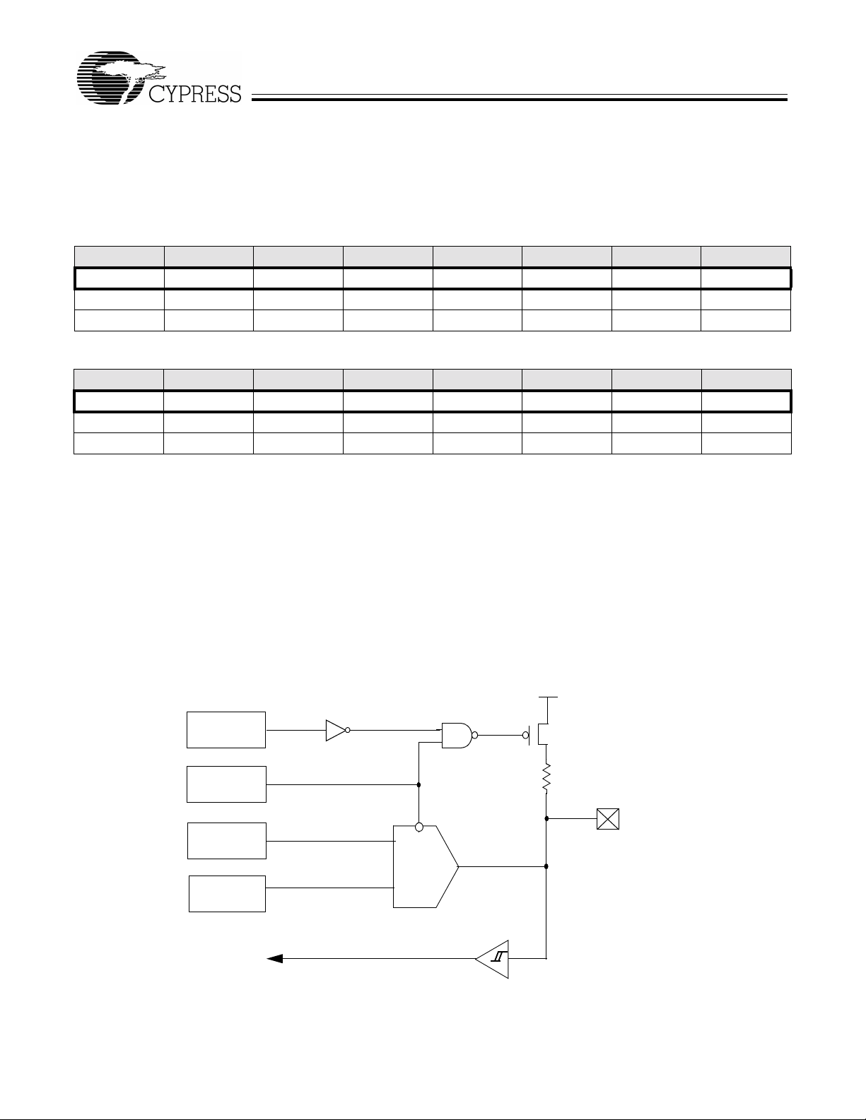
For Cex t to gen erate an “Instant-on” interrupt, the pin m u st be conn ec ted to gro und with an external capacitor and conne cte d to
with an external resistor. A “0” is written to the C ext register located at I/O address 0x2 2 t o discharge the capac ito r. Then, a
V
CC
“1” is written to disable the open-drain output driver. A Schmitt trigger input circuit monitors the input and generates a wake-up
interrupt when the input voltage rises above the input threshold. By changing the values of the external resistor and capacitor,
the user can f i n e t une t he c ha rge ra te of t he R- C t i ming c ir c ui t . Th e for ma t of th e C ext re gi ste r is sh own i n
the register returns the value of the Cext pin. During a reset, the Cext pin is HIGH.
b7 b6 b5 b4 b3 b2 b1 b0
Reserved Reserved Reserved Reserved Reserved Reserved Reserved CEXT
0 0 0 0 0 0 0 1
Figure 5-5. The Cext Register (Address 0x22)
Figure 5-5
. Reading
R/W
5.5 On-Chip Timer
The USB Controller is equip ped with a free-running timer driv en b y a cloc k one-s ixth the res onato r frequenc y. Bits 0 through 7 of
the counter are readable from the read-only Timer Register located at I/O address 0x23. The Timer Register is cleared during a
Power-On Reset and whenever Suspend mode is entered.
block diagram.
With a 6 MHz resonator, the timer resolution is 1 µs.
The timer generates two interrupts: the 128-µs interrupt and the 1.024-ms interrupt.
b7 b6 b5 b4 b3 b2 b1 b0
T.7 T.6 T.5 T.4 T.3 T.2 T.1 T.0
R R R R R R R R
0 0 0 0 0 0 0 0
Figure 5-6. Timer Register (Address 0x23)
Figure 5-6
illustrates the for mat of this register and
Figure 5-7
is its
1.024-ms interrupt
m
128-
9
8
7
6
5
4
3
2
1
0
s interrupt
Resonator Clock/6
Figure 5-7. Timer Block Diagram
11
8
To Timer Register
Page 12
FOR
FOR
CY7C63000A/CY7C63001A
CY7C63100A/CY7C63101A
5.6 General Purpose I/O Ports
Interface wit h peripher als is c onducted via as man y as 16 GPIO sig nals . These si gnals are divided i nto tw o ports: P ort 0 and P ort
1. Port 0 contains eight lines (P0.0–P0.7) and Por t 1 contains up to eight lines (P1.0–P1.7). The number o f extern al I/O pi ns
depends on the p ackage type . Both p orts can b e ac ce ss ed by the IORD, IOWR, and IO WX instructions . T he Port 0 data regist er
is located at I/O address 0x00 w hile the P o rt 1 data register is located at I/O add ress 0x01. The contents of both registers are s et
HIGH during a reset. Ref er to
put functions, each I/O line can trigger an interrupt to the microcontroller. Please refer to the interrupt section for more details.
b7 b6 b5 b4 b3 b2 b1 b0
P0.7 P0.6 P0.5 P0.4 P0.3 P0.2 P0.1 P0.0
R/W R/W R/W R/W R/W R/W R/W R/W
1 1 1 1 1 1 1 1
b7 b6 b5 b4 b3 b2 b1 b0
P1.7 P1.6 P1.5 P1.4 P1.3 P1.2 P1.1 P1.0
R/W R/W R/W R/W R/W R/W R/W R/W
1 1 1 1 1 1 1 1
Figures 5-8
Figure 5-8. Port 0 Data Register (Address 0x00)
Figure 5-9. Port 1 Data Register (Address 0x01)
and
5-9
for the f ormats of the data registers . In addition to supporting general inpu t/out-
Each GPIO line includes an internal R
govern the enabling and disabling of each resistor: the state of its associated Port Pull-up register bit and the state of the Data
resistor. This resistor provides both the pull-up function and slew control. Two factors
up
Register bit. NOTE: The control bits in the Port Pull-up register are active LOW.
A GPIO line is HIGH when a “1” is w ritten to the Data Register an d a “0” is written to the respective Port Pull-up regis ter. Writing
a “0” to the port Data Register disables the port’s Pull-up resistor and outputs a LOW on the GPIO line regardless of the setting
in the Port Pull-up Register. The output goes to a high-Z state if the Data Register bit and the Port Pull-up Register bit are both
Figure 5-10
“1”.
illustrates the b loc k diag ram of on e I/O line . The P ort Isink Regi ster is use d to control th e output curre nt le ve l and
it is described later in thi s sec t ion . NOTE: The Isink logic block is turned off d uring su spend mode (please refer to the Insta nt-on
Feature section for more details). Therefore, to prevent higher I
Port 0 and Por t 1 Data Register bits (which are not externally driven to a known state),
out on a particular package
the Suspend bit (bit 3 of the Status and Control Register).
, to “1” and all P ort 0 and Port 1 Pull-Up Regis ter data bits to “0” to enab le port pull-ups bef ore setting
Table 5-2
currents during USB suspend mode, firmware must set ALL
CC
including those that are not bonded
is the Output Control truth table.
V
CC
Port Pul l-Up
Register
R
Port Data
up
Register
GPIO
Port Isink
Register
Suspend
Isink
DAC
Disable
Pin
Bit
Schmitt
Trigger
Data Bus
Figure 5-10. Block Diagram of an I/O Line
12
Page 13

FOR
FOR
CY7C63000A/CY7C63001A
CY7C63100A/CY7C63101A
T a b le 5-2. Output Control Truth Table
Data Register Port Pull-up Register Output at I/O Pin Interrupt Polarity
0 0 Sink Current (‘0’) High to Low
0 1 Sink Current (‘0’) Low to High
1 0 Pull-up Resistor (‘1’) High to Low
1 1 Hi-Z Low to High
To configure a GPIO pin as an input, a “1” should be written to the Port Data Register bit associated with that pin to disable the
pull-down function of the Isink DAC (see
the pin is greater than the Schmitt trigger threshold, or “0” if it is below the threshold. In applications where an internal pull-up is
required, the R
pull-up resistor can be engaged by writing a “0” to the appropriate bit in the Port Pull-Up Register.
up
Both Port 0 and P ort 1 Pull-up Registers are write only (see
address 0x08 and Por t 1 Pull-up Register is mapped to address 0x09. The contents of the Port Pull-up Registers are cleared
during reset, allowing the outputs to be controlled by the state of the Data Registers. The Port Pull-up Registers also select the
polarity of transition that generates a GPIO interrupt. A “0” selects a HIGH to LOW transition while a “1” selects a LOW to HIGH
transition.
b7 b6 b5 b4 b3 b2 b1 b0
PULL0.7 PULL0.6 PULL0.5 PULL0.4 PULL0.3 PULL0.2 PULL0.1 PULL0.0
W W W W W W W W
0 0 0 0 0 0 0 0
Figure 5-10
).When the P ort Data Regis ter is read, the bit v alue is a “1” if the vo lta ge o n
Figures 5-11
and
5-12
). The Port 0 Pull-up Registe r is loca ted at I/O
Figure 5-11. Port 0 Pull-Up Register (Address 0x08)
b7 b6 b5 b4 b3 b2 b1 b0
PULL1.7 PULL1.6 PULL1.5 PULL1.4 PULL1.3 PULL1.2 PULL1.1 PULL1.0
W W W W W W W W
0x 0 0 0 0 0 0 0
Figure 5-12. Port 1 Pull-Up Register (Address 0x09)
Writing a “0” to the Data Regis ter d riv e s th e ou tpu t LOW. Instead of providing a fixed ou tpu t drive, the USB Cont rol ler a llows the
user to select an o utp ut s ink c urren t level for each I/O pin. The sink current of each outp ut i s c ont roll ed by a dedicated Port Isink
Register. The lower four bits of th is register contain a cod e s el ecting one of sixte en si nk current le vels. The up per four bits of the
register are ignored. The format of the Port Isink Register is shown in
Figure 5-13
.
b7 b6 b5 b4 b3 b2 b1 b0
Reserved Reserved Reserved UNUSED ISINK3 ISINK2 ISINK1 ISINK0
W W W W W W W W
x x x x x x x x
Figure 5-13. Port Isink Register for One GPIO Line
Port 0 is a low-current port suitable for connecting photo transistors. Port 1 is a high current port capable of driving LEDs. See
section 7.0 for current ranges. 0000 is the lowest drive strength. 1111 is the highest.
The write-only sink current control registers for Por t 0 outputs are assigned from I/O address 0x30 to 0x37 with the control bits
for P00 sta rting at 0x30 . Port 1 sink current c on trol reg is ters are as s ign ed from I/ O address 0x38 to 0x3 F w i th the co ntro l bits for
P10 starting at 0x38. All sink current control registers are cleared during a reset, resulting in the minimum current sink setting.
5.7 XTALIN/XTALOUT
The XTALIN and XTALOUT pins support connection of a 6 MHz ceramic resonator. The feedback capacitors and bias resistor
are internal to the IC, as shown in
Figure 5-14
Leave XTALOUT unconnected when driving XTALIN from an external oscillator.
13
Page 14

FOR
FOR
CY7C63000A/CY7C63001A
CY7C63100A/CY7C63101A
XTALOUT
clk1x
(to USB SIE)
clk2x
(to Microcontroller)
5.8 Interrupts
Interrupts are generated b y the Gene ral Purpose I/O line s, the Cext pin, the internal timer, and the USB e ngine . Al l inte rrupts are
maskable b y the Global Interrupt Enab le Register . Access to this reg ister is accomplished v ia IORD , IOWR, and I OWX instruction s
to address 0x20. Writing a “1” to a bit position enable s the interrupt associated with t hat p os itio n. D uring a rese t, th e contents of
the Interrupt Enable Registe r are cl eared, d isab ling a ll int errupts.
Register.
b7 b6 b5 b4 b3 b2 b1 b0
CEXTIE GPIOIE Reserved EP1IE EP0IE 1024IE 128IE Reserved
R/W R/W R/W R/W R/W R/W
0 0 0 0 0 0 0 0
Figure 5-15. Global Interrupt Enable Register (GIER - Address 0x20)
The interrupt controller contains a separate latch for each interrupt. See
controller . Wh en an in terrupt is ge nera ted , it is latc hed as a pendin g interrupt. I t stays as a pend ing int errupt until i t is serviced or
a reset occurs. A pending interrupt onl y gener ates an inte rrupt request i f it is e nabl ed in the Global Interrupt Enab le Regi ster. The
highest priority interrupt request is serviced following the execution of the current instruction.
When servicing an interrupt, the hardware first disables all interrupts by clearing the Global Interrupt Enable Register. Next, the
interrupt latch of the current interrupt is cleared. This is followed by a CALL instruction to the ROM address associated with the
interrupt being serviced (i.e., the interrupt v ector). The instructi on in the interrupt table is typi cally a JMP instruction to the address
of the Interrupt Service Routine (ISR). The user can re-enable interrupts in the interrupt service routine by writing to the appropriate bits in the Global Interrupt Enable Register. Interrupts can be nested to a level limited only by the available stack space.
Clock
Doubler
30 pF30 pF
Figure 5-14. Clock Oscillator On-Chip Circuit
Figure 5-15
illustrates the format of the Global Interrupt Enab l e
Figure 5-16
XTALIN
for the logic block diagram for the interrupt
Global
Interrupt
Enable
Register
CLR
Interrupt
Acknowledge
CLR
Logic 1
128-ms
Interrupt
Enable [7:0]
Logic 1
GPIO
Interrupt
Logic 1
CEXT
DQ
CLK
CLR
DQ
CLK
CLR
DQ
CLK
Enable [1]
Enable [6]
Enable [7]
Figure 5-16. Interrupt Controller Logic Block Diagram
14
128-ms CLR
128-ms IRQ
1-ms CLR
1-ms IRQ
End P0 CLR
End P0 IRQ
End P1 CLR
End P1 IRQ
GPIO CLR
GPIO IRQ
Wake-up CLR
Wake-up IRQ
Interrupt
Priority
Encoder
IRQ
Interrupt
Vector
Page 15

FOR
FOR
CY7C63000A/CY7C63001A
CY7C63100A/CY7C63101A
The Program Counter (PC) value and the Carry and Zero flags (CF, ZF) are automatic all y st ored onto the Prog r am Stack by the
CALL instruction as part of the interrupt acknowledge process. The user firmware is responsible for ensuring that the processor
state is preserved and restore d during an interrupt. F o r e xample th e PUSH A instruction sho uld be us ed as the first co mmand in
the ISR to save the accumulator value. And, the IPRET instruction should be used to exit the ISR with the accumulator value
restored and interrupts enabled. The PC, CF, and ZF are restored when the IPRET or RET instructions are executed.
The Interrupt Vectors supported by the USB Controller are listed in
Interrupt Vector 7 has the lowest priority. Because the JMP instruction is 2 bytes long, the interrupt vectors occupy 2 bytes.
Table 5-3. Interrupt Vector Assignments
Interrupt Priority ROM Address Function
0 (Highest) 0x00 Reset
1 0x02 128-µs timer interrupt
2 0x04 1.024-ms timer interrupt
3 0x06 USB endpoint 0 interrupt
4 0x08 USB endpoint 1 interrupt
5 0x0A Reserved
6 0x0C GPIO interrupt
7 (Lowest) 0x0E Wake-up interrupt
Table 5-3
. Interrupt Vector 0 (Reset) has the highest priority,
5.8.1 Interrupt Latency
Interrupt latency can be calculated from the following equation:
Interrupt Latency = (Number of clock cycles remaining in the current instruction) + (10 clock cycles for the CALL instruction) +
(5 clock cycles for the JMP instruction)
For example, if a 5-clock-cycle instruction such as JC is being executed when an interrupt occurs, the first instruction of the
Interrupt Service Routine executes a minimum of 16 clock cycles (1+10+5) or a maximum of 20 clock cycles (5+10+5) after the
interrupt is issued. Therefore, the interrupt latency in this example will be = 20 clock periods = 20 / (12 MHz) = 1.667 µs. The
interrupt latches are sampled at the rising edge of the last clock cycle in the current instruction.
5.8.2 GPIO Interrupt
The General Purpose I/O in terrupts are gener ated by s ignal tran sitions at th e P ort 0 and P ort 1 I/O pins. GPIO in terrupts are edge
sensitive wi th programma ble interrupt polaritie s. Setting a bit HIGH in the P ort Pull-up Register (see
Figure 5-11
and
5-12
) selects
a LOW to HIGH interrupt trigger f or the corre sponding port pin. Setting a bit LO W activ ates a HIGH to LO W interrupt trigger . Each
GPIO interrupt is maskable on a per-pin basis by a dedicated bit in the Port Interrupt Enable Register. Writing a “1” enables the
interrupt.
Figure 5-17
and
Figure 5-18
illustrate the format of the Port Interrupt Enable Registers for Port 0 and Port 1 located at
I/O address 0x04 and 0x05 respectively. These write only registers are cleared during reset, thus disabling all GPIO interrupts.
b7 b6 b5 b4 b3 b2 b1 b0
IE0.7 IE0.6 IE0.5 IE0.4 IE0.3 IE0.2 IE0.1 IE0.0
W W W W W W W W
0 0 0 0 0 0 0 0
Figure 5-17. Port 0 Interrupt Enable Register (P0 IE - Address 0x04)
b7 b6 b5 b4 b3 b2 b1 b0
IE1.7 IE1.6 IE1.5 IE1.4 IE1.3 IE1.2 IE1.1 IE1.0
W W W W W W W W
0 0 0 0 0 0 0 0
Figure 5-18. Port 1 Interrupt Enable Register (P1 IE - Address 0x05)
A block diagram of the GPIO interrupt logic is shown in
Figure 5-19
. The bit setting i n the P ort Pull-up Register selects the interrupt
polarity. If the selected signal polarity is detected on the I/O pin, a HIGH signal is generated. If the Port Interrupt Enable bit for
this pin is HIGH and no other port pins are requesting interrupts, the OR gate issues a LOW to HIGH signal to clock the GPIO
interrupt flip-flop. The output of the flip-flop is further qualified by the Global GPIO Interrupt Enable bit before it is processed by
15
Page 16

FOR
FOR
CY7C63000A/CY7C63001A
CY7C63100A/CY7C63101A
the Interrupt Priority Encoder. Both the GPIO interrupt flip-flop and the Global GPIO Enable bit are cleared by on-chip hardware
during GPIO interrupt acknowledge.
GPIO
Pin
1 = Enable
0 = Disable
Interrupt
Acknowledge
Port
Pull-Up
Register
M
U
X
Port Interrupt
Enable Register
1 = Enable
0 = Disable
(Bit 6, Register 0x20)
→
H
1=L
0=H
L
Æ
CLR
Global
GPIO Interrupt
Enable
OR Gate
(1 input per
GPIO pin)
GPIO Interrupt
Flip-Flop
I
D
CLR
Q
Interrupt
Priority
Encoder
IRQ
Interrupt
Vector
Figure 5-19. GPIO Interrupt Logic Block Diagram
NOTE: If on e port pin triggers an interrupt, no other port pin can cause a GPIO interrupt unt il the port pin that triggered the in terrupt
has returned to its inactive (non-trigger) state or until its corresponding port interrupt enable bit is cleared (these events ‘reset’
the clock of the GPIO Interrupt flip-flop, which must be ‘reset’ to ‘0’ before another GPIO interrupt event can ‘clock’ the GPIO
Interrupt flip-flop and produce an IRQ).
NOTE: If the po rt pin that t riggered an int errupt is he ld in its activ e (trigge r) s tate w hil e i ts c orre sp ond in g po rt interrupt enable bit
is cleared and then s et, a GPIO inte rrupt e v ent occurs as the GPIO I nterrupt flip-flo p cloc k tran sitions f rom ‘1’ to ‘0’ and t hen bac k
to ‘1’ (please refer to
Figure 5-19
). The USB Controller does not as sign interrupt priority to diff erent port pins and the P ort Interrupt
Enable Registers are not cleared during the interrupt acknowledge process. When a GPIO interrupt is serviced, the ISR must
poll the ports to determine which pin caused the interrupt.
5.8.3 USB Interrupt
A USB Endpoint 0 interrupt is gen erate d after th e host h as written da ta to Endp oint 0 or a fter the USB Control ler has trans mitted
a packet from Endp oint 0 and receiv es an ACK from the host. An OUT packet from t he host which is NAK ed by the USB Controll er
does not generate a n interrupt. This interrupt is mas ked b y the U SB EP0 Interrupt En able bit (bit 3) o f the Global Interrupt Enable
Register.
A USB Endpoint 1 inte rrupt is ge ne ra ted aft er the USB Controller has tr a ns mit ted a packet from End point 1 and has rece ived an
ACK from the host. This interrupt is masked by the USB EP1 Interrupt Enable bit (bit 4) of the Global Interrupt Enable Register.
5.8.4 Timer Interrupt
There are two timer interrupts: the 128-µs interrupt and the 1.024-ms interrupt. They are masked by bits 1 and 2 of the Global
Interrupt Enable Reg ister resp ectiv ely. The user should disa ble both time r interrupts be for e goin g into the suspend mode to av oid
possible conflicts from timer interrupts occurring just as suspend mode is entered.
5.8.5 Wake-Up Interrupt
A wake-up interrupt is generated when the Cext pin goes HIGH. This interrupt is latched in the interrupt controller. It can be
masked by the W ak e -up Interrupt Ena ble bit (bit 7) of th e Global Int errupt Enab le Register. This interrupt can be used to perform
periodic checks on atta ched pe ripher als when the USB Contro ller is pl aced in the low- po wer su spend mode . See the Ins tant-O n
Feature section for more details.
5.9 USB Engine
The USB engine includ es the Serial Interf ace Engine (SIE) and the l ow-speed USB I/O tr ansceiv ers. The SIE b lock perf orms most
of the USB interfac e func tions wi th only minimal support from the micr ocon troller core . Two endpoints are supported. Endpoin t 0
is used to receive and transmit control (including setup) packets while Endpoint 1 is only used to transmit data packets.
16
Page 17

FOR
FOR
CY7C63000A/CY7C63001A
CY7C63100A/CY7C63101A
The USB SIE processes USB bus activity at the transaction level independently. It does all the NRZI encoding/decoding and bit
stuffing/unstuffing. It also determin es token type, checks address and endpoint values, generates and checks CRC values, and
controls the flow of d ata bytes bet ween the b us and the Endpo int FIFOs. NOTE: th e SIE stalls the CPU for 3 cycl es per byt e when
writing data to the endpoint FIFOs (or 3 * 1/12 MHz * 8 bytes = 2 µs per 8-byte transfer).
The firmware handles hig her lev el and function-spe cific tasks. During co ntrol transf ers the firmware must in terpret device requ ests
and respond correctly. It also must coordinate Suspend/Resume, verify and select DATA toggle values, and perform function
specific tasks.
The USB engine and the firmware communicate though the Endpoint FIFOs, USB Endpoint interrupts, and the USB registers
described in the sections below.
5.9.1 USB Enumeration Process
The USB Controller provides a USB Device Address Register at I/O location 0x12. Reading and writing this register is achieved
via the IORD and IOWR instructions. The register contents are cleared during a reset, setting the USB address of the USB
Controller to 0.
b7 b6 b5 b4 b3 b2 b1 b0
Reserved ADR6 ADR5 ADR4 ADR3 ADR2 ADR1 ADR0
0 0 0 0 0 0 0 0
Figure 5-20
shows the format of the USB Address Register.
R/W R/W R/W R/W R/W R/W R/W
Figure 5-20. USB Device Address Register (USB DA - Address 0x12)
Typical enumeration steps:
1. The host computer sends a SETUP packet followed by a DATA packet to USB address 0 requesting the Device descriptor.
2. The USB Controller decodes the request and retrieves its Device descriptor from the program memory space.
3. The host compu ter perfo rms a control read sequ ence and the U SB Controller res ponds b y sending the D evice d escriptor ov er
the USB bus.
4. After receiving the descriptor, the host computer sends a SETUP packet f ol lo we d by a D ATA packet to address 0 assigning a
new USB address to the device.
5. The USB Controller stores the new address in its USB Device Add ress Register afte r the no-data control sequenc e completes .
6. The host sends a request for the Device descriptor using the new USB address.
7. The USB Controller decodes the request and retrieves the Device descriptor from the program memory.
8. The host perf orms a control read sequence and the USB Controll er responds by sending its De vice descriptor ove r the USB bus.
9. The host generates control reads to the USB Controller to request the Configuration and Report descriptors.
10.The USB Controller retrieves the descriptors from its program space and returns the data to the host over the USB.
11.Enumeration is complete after the host has received all the descriptors.
5.9.2 Endpoint 0
All USB devic es are required to ha ve an end point number 0 that is used to initial ize and mani pulate the de vice. Endpoint 0 provides
access to the device’s configuration information and allows generic USB status and control accesses.
Endpoint 0 can receiv e and transm it data. Both receiv e and tr ansmit data share the same 8-byt e Endpoint 0 FIFO located at data
memory space 0x70 to 0x77. Received data may overwrite the data previously in the FIFO.
5.9.2.1 Endpoint 0 Receive
After receiving a packet and placing the data into the Endpoint 0 FIFO, the USB Controller updates the USB Endpoint 0 RX
register to record the receive status and then generates a USB Endpoint 0 interrupt. The format of the Endpoint 0 RX Register
is shown in
Figure 5-21
.
b7 b6 b5 b4 b3 b2 b1 b0
COUNT3 COUNT2 COUNT1 COUNT0 TOGGLE IN OUT SETUP
Figure 5-21. USB Endpoint 0 RX Register (Address 0x14)
17
Page 18

FOR
FOR
CY7C63000A/CY7C63001A
CY7C63100A/CY7C63101A
R/W R/W R/W R/W R R/W R/W R/W
0 0 0 0 0 0 0 0
Figure 5-21. USB Endpoint 0 RX Register (Address 0x14)
This is a read/write register located at I/O address 0x14. Any write to this register clears all bits except bit 3 which remains
unchanged. All bits are cleared during reset.
Bit 0 is set to 1 when a SETUP token for Endpoint 0 is received. Once set to a 1, this bit remains HIGH until it is cleared by an
I/O write or a reset. Wh ile the data following a SETUP is being receive d b y the USB eng ine , this bit is not c leared b y an I/O w rite.
User firmware writes to the USB FIFOs are disabled when bit 0 is set. This prevents SETUP data from being overwritten.
Bits 1 and 2 a re updated wh ene ver a v alid t oken i s receiv ed on Endpo int 0. Bit 1 is set to 1 if an OUT tok en is receiv ed an d cleared
to 0 if any other token is received. Bit 2 is set to 1 if an IN token is received and cleared to 0 if any other token is received.
Bit 3 shows the Data Toggle status of D ATA packets receiv ed on End point 0. Th is bit is up dated f or D ATA following SETUP to kens
and for DATA following OUT tokens if Stall (bit 5 of 0x10) is not set and either EnableOuts or StatusOuts (bits 3 and 4 of 0x13)
are set.
Bits 4 to 7 are the count of the number of bytes received in a DATA packet. The two CRC bytes are included in the count, so the
count value is two greater than the n um be r of d ata b y tes rec ei ved. The count is al ways updated and the data is always stor ed i n
the FIFO for D ATA packets foll owing a SET UP tok en. The co unt f or D ATA following an OUT toke n is update d if Stall (bi t 5 of 0x10)
is 0 and either EnableOuts or StatusOuts (bits 3 and 4 of 0x13) are 1. The DATA following an OUT is written into the FIFO if
EnableOuts is set to 1 and Stall and StatusOuts are 0.
A maximum of 8 b ytes are written into t he Endpoin t 0 FIFO. If there are less than 8 bytes of data the CRC is w ritten into the FIFO.
Due to register space limitations, the Receive Data Invalid bit is located in the USB Endpoint 0 TX Configuration Register. Refer
to the Endpoint 0 Transmit section for details. This bit is set by the SIE if an error is detected in a received DATA packet.
Table 5-4
‘Error’ represents a packet with a CRC, PID or bit-stuffing error, or a packet with more than 8 bytes of data. ‘Valid’ is a packet
without an Error. ‘Status’ is a packet that is a valid control read Status stage, while ‘N/Status’ is not a correct Status stage (see
section 5.9.4). The ‘Stall’ bit is described in Section 5.9.2.2. The ‘StatusOuts’ and ‘EnableOuts’ bits are described in section 5.9.4.
summarizes the USB Engine response to SETUP and OUT transactions on Endpoint 0. In the Data Packet column
T a b le 5-4. USB Engine Response to SETUP and OUT Transactions on Endpoint 0
Control Bit Settings Received Packets USB Engine Response
Stall Status Out Enable Out Token Type Data
Packet
FIFO Write Toggle
Update
Count
Update
Interrupt Reply
- - - SETUP Valid Yes Yes Yes Yes ACK
- - - SETUP Error Yes Yes Yes Yes None
0 0 1 OUT Valid Yes Yes Yes Yes ACK
0 0 1 OUT Error Yes Yes Yes Yes None
0 0 0OUTValidNoNoNoNoNAK
0 0 0OUTErrorNoNoNoNoNone
1 0 0OUTValidNoNoNoNoSTALL
1 0 0OUTErrorNoNoNoNoNone
0 1 0 OUT Status No Yes Yes Yes ACK
0 1 0 OUT N/Status No Yes Yes Yes STALL
0 1 0 OUT Error No Yes No No None
5.9.2.2 Endpoint 0 Transmit
The USB Endpoint 0 TX Regis ter locate d at I/O addre ss 0x10 cont rols data tr ansmis sion from En dpoint 0 (se e
Figure 5-22
is a read/write register. All bits are cleared during reset.
b7 b6 b5 b4 b3 b2 b1 b0
INEN DA T A1/0 STALL ERR COUNT3 COUNT2 COUNT1 COUNT0
Figure 5-22. USB Endpoint 0 TX Configuration Register (Address 0x10)
). This
18
Page 19

FOR
FOR
CY7C63000A/CY7C63001A
CY7C63100A/CY7C63101A
R/W R/W R/W R/W R/W R/W R/W R/W
0 0 0 0 0 0 0 0
Figure 5-22. USB Endpoint 0 TX Configuration Register (Address 0x10)
Bits 0 to 3 indicate the numbers of data b ytes to be trans mitted during an IN pac ket, v alid valu es are 0 to 8 inclus ive. Bit 4 indicates
that a received D ATA packet error (CRC, PID, or bitstuffing error) occurred during a SETU P or OUT data phase . Settin g the Stall
bit (bit 5) stalls IN and OUT packets. This bit is cleared whenever a SETUP packet is received by Endpoint 0. Bit 6 (Data 1/0)
must be set to 0 or 1 to select the DATA packet’s toggle state (0 for DATA0, 1 for DATA1).
After the transmit data has been loaded into the FIFO, bit 6 should be set according to the data toggle state and bit 7 set to “1”.
This enables the USB C on troll er to res pon d to an I N packet. Bit 7 is c lea red a nd a n En dpo int 0 interrupt is generat ed by the SIE
once the host acknowledges the data transmission. Bit 7 is also cleared when a SETUP token is received. The Interrupt Service
Routine can check bit 7 to confirm that the data transfer was successful.
5.9.3 Endpoint 1
Endpoint 1 is capab le of tr ansmit on ly. The data to be transmitted is s tored in the 8-b yte En dpoint 1 FIFO located a t data memo ry
space 0x78 to 0x7F.
5.9.3.1 Endpoint 1 Transmit
Transmission is controlled b y the USB En dpoint 1 T X Re gister loca ted a t I /O addre ss 0 x11 (see
register. All bits are cleared during reset.
Figure 5-23
). This is a rea d/write
b7 b6 b5 b4 b3 b2 b1 b0
INEN DATA1/0 STALL EP1EN COUNT3 COUNT2 COUNT1 COUNT0
R/W R/W R/W R/W R/W R/W R/W R/W
0 0 0 0 0 0 0 0
Figure 5-23. USB Endpoint 1 TX Configuration Register (Address 0x11)
Bits 0 to 3 indicate the numbers of data bytes to be transmitted during an IN packet, valid values are 0 to 8 inclusive.
Bit 4 must be set before Endpoint 1 can be used. If this bit is cleared, the USB Controller ignores all traffic to Endpoint 1.
Setting the Stall bit (bit 5) stalls IN and OUT packets until this bit is cleared.
Bit 6 (Data 1/0) must be set to either 0 or 1 depending on the data packet’s toggle state, 0 for DATA0, 1 for DATA1.
After the transmit data has been loaded into the FIFO, bit 6 should be set according to the data toggle state and bit 7 set to “1”.
This enables the USB C on troll er to res pon d to an I N packet. Bit 7 is c lea red a nd a n En dpo int 1 interrupt is generat ed by the SIE
once the host acknowledges the data transmission.
5.9.4 USB Status and Control
USB status and control is regulated by USB Status and Control Register located at I/O address 0x13 as shown in
Figure 5 -24
This is a read/write register. All reserved bits must be written to zero. All bits in the register are cleared during reset.
b7 b6 b5 b4 b3 b2 b1 b0
Reserved Reserved Reserved ENOUTS STATOUTS FORCEJ FORCEK BUSACT
R/W R/W R/W R/W
0 0 0 0 0 0 0 0
Figure 5-24. USB Status and Control Register (USB SCR - Address 0x13)
.
Bit 0 is set by the SIE if any USB activity except idle (D+ LOW, D– HIGH) is detected. The us er pro gram should check and clear
this bit periodically to detect any loss of bus activity. Writing a 0 to this bit clears it. Writing a 1 does not change its value.
Bit 1 is used to force the on-chip USB transmitter to the K state which sends a Resume signal to the host. Bit 2 is used to force
the transmitter to the J state. This bit should normally be set to zero. However, for resume signaling, force a J state for one
instruction before forcing resume.
Bit 3 is used to automatica lly respond to the Status stag e OUT of a contr ol read tran sf er on Endpoint 0. A v alid Status sta ge OUT
contains a D ATA1 packet with 0 bytes of dat a. If the Status O uts bit is set , the USB eng ine resp ond s to a valid Status stage OUT
with an ACK, and an y oth er OUT wit h a STALL. The data is not written into the FIFO whe n this bit is s et. This bit is c leared wh en
a SETUP token is received by Endpoint 0.
19
Page 20

FOR
FOR
CY7C63000A/CY7C63001A
CY7C63100A/CY7C63101A
Bit 4 is used to enable the receiving of Endpoint 0 OUT packets. When this bit is set to 1, the data from an OUT transaction is
written into the Endpoint 0 FIFO . If this bit is 0, data is not written to the FIFO and the SIE responds with a NAK. This bit is cl eared
following a SETUP or ACKed OUT transaction. NOTE: After firmware decodes a SETUP packet and prepares for a subsequent
OUT transaction by setting bit 4, bit 4 is not cleared until the hand-shake phase of an ACKed OUT transaction (a NAKed OUT
transaction does not clear this bit).
5.10 USB Physical Layer Characteristics
The following section describes the CY7C630/1XXA compliance to the Chapter 7 Electrical section of the USB Specification,
Revision 1.1. Th e sectio n contai ns all s ignalin g, pow er dist ributio n, and ph ys ical la y er sp ecificat ions nec essary to des cribe a lowspeed USB function.
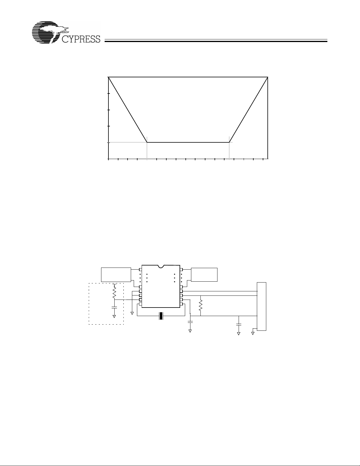
5.10.1 Low-Speed Driver Characteristics
The CY7C630/1XXA devices use a differential output driver to drive the Low Speed USB data signal onto the USB cable, as
shown in
Slew rate control on the driver minimizes the radiated noise and cross talk on the USB cable. The driver’s outputs support
three-state operation to achieve bidirectional half duplex operation. The CY7C630/1XXA driver tolerates a voltage on the signal
pins of –0.5V to 3.8V with respect to local ground reference without damage. The driver tolerates this voltage for 10.0 µs while
the driver is active and driving, and tolerates this condition indefinitely when the driver is in its high-impedance state.
A low-speed USB connection is made through an unshielded, untwisted wire cable a maximum of 3 meters in length. The rise
and fall time of the signals on this cable are well controlled to reduce RFI emissions while limiting delays, signaling skews and
distortions. The CY7C630/1XXA driver reaches the specified static signal levels with smooth rise and fall times, resulting in
minimal reflections and ringing when driving the USB cable. This cable and driver are intended to be used only on network
segments between low-speed devices and the ports to which they are connected.
Figure 5-25
. The output swings between the differential high and low state are well balanced to minimize signal skew.
One Bit
Time
(1.5Mb/s)
(max)
V
SE
Driver
Signal Pins
(min)
VSE
VSS
Signal pins
pass output
spec levels
with minimal
reflections and
ringing
Figure 5-25. Low Speed Driver Signal Waveforms
5.10.2 Receiver Characteristics
The CY7C630/1XXA has a differential input receiver which is able to ac cept the USB data signal. The receiv e r features an input
sensitivity of at least 200 mV when both differential data inputs are in the range of at least 0.8V to 2.5V with respect to its local
ground reference. This is the common mode input voltage range. Proper data reception is also guaranteed when the differential
data lines are outside the common mode range, as shown in
Figure 5-26
. The receiver to lerat es stat ic inp ut voltag es bet ween
–0.5V and 3.8V with respect to its local ground reference without damage. In addition to the differential receiver, there is a
20
Page 21
FOR
FOR
CY7C63000A/CY7C63001A
CY7C63100A/CY7C63101A
single-ended receiver for each of the two data lines. The single-ended receivers have a switching threshold between 0.8V and
2.0V (TTL inputs).
1.0
0.8
0.6
0.4
0.2
Minimum Differential Sensitivity (volts)
0.0
0.0 0.2 0.4 0.6 0.8 1.0 1.2 1.4 1.6 1.8 2.0 2.2 2.4 2.6 2.8 3.0 3.2
Common Mode Input Voltage (volts)
Figure 5-26. Differential Input Sensitivity Over Entire Common Mode Range
5.11 External USB Pull-Up Resistor
The USB system specifies that a pull-up resistor be connected on the D– pin of low-speed peripherals as shown in
To meet the USB 1.1 spec (section 7.1.6), whic h st ates that the termination mus t ch arge the D- l ine from 0 to 2 .0 V in 2.5µs, the
total load capacitance on the D+/D - li nes of the lo w sp eed USB device (Cypress device capacita nc e + PCB trac e ca pac itance +
integrated cab le capacitance) m ust be less than 250pF. As Cypress D+/D - transceiv er input capacitance is 20pF max, up to 230pF
of capacitance is allowed for in the low speed device’s integrated cable and PCB. If the cable + PCB capacitance on the D+/D-
lines will be greater than approximately 230 pF, an external 3.3V regulator must be used as shown in
XTALOUT
6-MHz
Port0
Port1
D+
D–
VCC
0.1µF
Switches,
Devices, Etc.
7.5kW±1%
+4.35V (min)
4.7 µF
Switches,
Devices, Etc.
For Cext
Wake-up Mode
Port0
Port1
VSS
VPP
CEXT
XTALIN
Resonator
Figure 5-28
USB Connector
Figure 5-27
.
.
Figure 5-27. Application Showing 7.5k
21
Ω±1%
Pull-Up Resistor
Page 22

Switches,
Devices, Etc.
For Cext
Wake-up Mode
FOR
FOR
CY7C63000A/CY7C63001A
CY7C63100A/CY7C63101A
+3.3V
3.3V
Port0
Port1
V
SS
V
PP
CEXT
XTALIN
XTALOUT
6-MHz
Resonator
Port0
Port1
D+
D–
V
CC
0.1µF
Switches,
Devices, Etc.
Reg
0.1 µF
1.5±kW
+4.35V (min.)
4.7 µF
USB Connector
Figure 5-28. Application Showing 1.5k
Ω±5%
Pull-Up Resistor
5.12 Instruction Set Summary
T a b le 5-5. Instr uctio n Set Map
MNEMONIC operand opcode cycles MNEMONIC operand opcode cycles
HALT 00 7 NOP 20 4
ADD A,expr data 01 4 INC A acc 21 4
ADD A,[expr] direct 02 6 INC X x 22 4
ADD A,[X+expr] index 03 7 INC [expr] direct 23 7
ADC A,expr data 04 4 INC [X+expr] index 24 8
ADC A,[expr] direct 05 6 DEC A acc 25 4
ADC A,[X+expr] index 06 7 DEC X x 26 4
SUB A,expr data 07 4 DEC [expr] direct 27 7
SUB A,[expr] direct 08 6 DEC [X+expr] index 28 8
SUB A,[X+expr] index 09 7 IORD expr address 29 5
SBB A,expr data 0A 4 IOWR expr address 2A 5
SBB A,[expr] direct 0B 6 POP A 2B 4
SBB A,[X+expr] index 0C 7 POP X 2C 4
OR A,expr data 0D 4 PUSH A 2D 5
OR A,[expr] direct OE 6 PUSH X 2E 5
OR A,[X+expr] index 0F 7 SWAP A,X 2F 5
AND A,expr data 10 4 SWAP A,DSP 30 5
AND A,[expr] direct 11 6 MOV [expr],A direct 31 5
AND A,[X+expr] index 12 7 MOV [X+expr],A index 32 6
XOR A,expr data 13 4 OR [expr],A direct 33 7
XOR A,[expr] direct 14 6 OR [X+expr],A index 34 8
XOR A,[X+expr] index 15 7 AND [expr],A direct 35 7
CMP A,expr data 16 5 AND [X+expr],A index 36 8
CMP A,[expr] direct 17 7 XOR [expr],A direct 37 7
CMP A,[X+expr] index 18 8 XOR [X+expr],A index 38 8
22
Page 23

FOR
FOR
CY7C63000A/CY7C63001A
CY7C63100A/CY7C63101A
T a b le 5-5. Instr uctio n Set Map
MOV A,e x pr data 19 4 IOWX [X+expr] index 39 6
MOV A,[expr] direct 1A 5 CPL 3A 4
MOV A,[X+expr] index 1B 6 ASL 3B 4
MOV X,e x pr data 1C 4 ASR 3C 4
MOV X,[expr] direct 1D 5 RLC 3D 4
IPRET addr 1E 13 RRC 3E 4
XPAGE 1F 4 RET 3F 8
JMP addr 8x 5 JC addr Cx 5
CALL addr 9x 10 JNC addr Dx 5
JZ addr Ax 5 JACC addr Ex 7
JNZ addr Bx 5 INDEX addr Fx 14
6.0 Absolute Maximum Ratings
Storage Temperature ..........................................................................................................................................–65°C to +150°C
Ambient Temperature with Power Applied...............................................................................................................–0°C to +70°C
Supply Voltage on VCC Relative to VSS..................................................................................................................–0.5V to +7.0V
DC Input Voltage........................................................................................................................................... –0.5V to +V
DC Voltage Applied to Outputs in High-Z state............................................................................................. –0.5V to +VCC+0.5V
Max. Output Current into Port 1 Pins................................................................................................................................... 60 mA
Max. Output Current into Non-Port 1 Pins.......................................................................................................................... 10 mA
Power Dissipation..............................................................................................................................................................300 mW
Static Discharge Voltage ................................................................................................................................................... >2000V
Latch-up Current
[1]
.......................................................................................................................................................... >200 mA
CC
+0.5V
23
Page 24

FOR
FOR
CY7C63000A/CY7C63001A
CY7C63100A/CY7C63101A
7.0 Electrical Characteristics
f
= 6 MHz; Operating Temperature = 0 to 70°C, VCC = 4.0 to 5.25 volts
OSC
Parameter Min Max Units Conditions
General
I
CC
I
SB1
I
SB2
V
PP
t
start
t
watch
VCC Operating Supply Current 25 mA
Supply Current—Suspend Mode 20
µ
Supply Current—Start-up Mode 4 mA
Programming Voltage (disabled) –0.4 0.4 V
Resonator Start-up Interval 256
µ
Watch Dog Timer Period 7.168 8.192 ms
A Resonator off, D– > Voh min
s Ceramic resonator
Power On Reset
t
VCCS
VCC Slew 0.010 1000 ms Linear ramp on VCC pin to V
USB Interface
V
oh
V
ol
V
di
V
cm
V
se
C
in
I
lo
R
pu1
R
pu2
R
pd
Notes:
1. All pins specified for >200 mA positive and negative injection, except P1.0 is specified for >50 mA negative injection.
2. Cext at V
3. Part powers up in suspend mode, able to be reset by USB Bus Reset.
4. POR may re-occur whenever V
5. Level guaranteed for range of V
6. With R
7. Maximum matched capacitive loading allowed on D+ and D– (including USB cable and host/hub) is approximately 230 pF.
Static Output High 2.8 3.6 V 15kΩ ± 5% to Gnd
Static Output Low 0.3 V See Notes 5 and 6
Differential Input Sensitivity 0.2 V |(D+)–(D–)|, and
Differential Input Common Mode Range 0.8 2.5 V
Figure 5-26
Single Ended Receiver Threshold 0.8 2.0 V
Transceiver Input Capacitance 20 pF D+ to Vss; D- to Vss
Data Line (D+, D–) Leakage –10 10
External Bus Pull-up Resistance, D– pin 1.425 1.575 k
External Bus Pull-up Resistance, D– pin 7.425 7.575 k
External Bus Pull-down Resistance 14.25 15.75 k
or Gnd, Port 0 and Port1 at VCC.
CC
drops to approximately 2.5V.
CC
= 4.35V to 5.25V.
of 1.5 KW±5% on D– to 3.3V regulator.
pu1
CC
µ
A 0 V <(D+, D–)<3.3 V, Hi-Z State
Ω
1.5 kΩ ± 5% to 3.3V supply
Ω
7.5 kΩ ± 1% to Vcc
Ω
15 kΩ ± 5%
[5,6]
Figure 5-26
[7]
[2]
CC
[3, 4]
24
Page 25

FOR
FOR
CY7C63000A/CY7C63001A
CY7C63100A/CY7C63101A
7.0 Electrical Characteristi cs
(continued) f
= 6 MHz; Operating Temperature = 0 to 70°C, VCC = 4.0 to 5.25 volts
OSC
Parameter Min Max Units Conditions
General Purpose I/O Interface
R
up
I
sink0(0)
I
sink0(F)
I
sink1(0)
I
sink1(F)
I
range
I
lin
T
ratio
t
sink
I
max
P
max
V
ith
V
H
V
HCext
Pull-up Resistance 8 24 k
Port 0 Sink Current (0), lowest current 0.1 0.3 mA Vout = 2.0V DC, Port 0 only
Port 0 Sink Current (F), highest current 0.5 1.5 mA Vout = 2.0V DC, Port 0 only
Port 1 Sink Current (0), lowest current 1.6 4.8 mA Vout = 2.0V DC, Port 1 only
Port 1 Sink Current (F), highest current 8
24 mAmAVout = 2.0V DC, Port 1 only
5
Sink Current max./min. 4.5 5.5 Vout = 2.0V DC, Port 0 or 1
Differential Nonlinearity 0.5 l
Tracking Ratio Port1 to Port0 14.4 19.6 Vout = 2.0V
Current Sink Response Time 0.8
Port 1 Max Sink Current 60 mA Summed over all Port 1 bits
Port 1 & Cext Sink Mode Dissipation 25 mW Per pin
Input Threshold Voltage 45% 65% V
Input Hysteresis Voltage 6% 12% V
Input Hysteresis Voltage, Cext 12% 30% V
Ω
Vout = 0.4V DC, Port 1 only
Port 0 or Port 1
SB
µ
s Full scale transition
All ports and Cext
CC
Port 0 and Port 1
CC
Cext Pin Only
CC
[10]
[12]
[5]
[5]
[5]
[5]
[5]
[5, 8]
[9]
[11]
[12]
Iin Input Leakage Current, GPIO Pins –11µA Port 0 and Port 1, Vout = 0 or V
I
inCx
I
Cext
V
ol1
V
ol2
8. I
range
9. Measured as largest step size vs. nominal according to measured full scale and zero programmed values
10. T
ratio
11. Low to High transition.
12. This parameter is guaranteed, but not tested.
13. With Ports configured in Hi-Z mode.
Input Leakage Current, Cext Pin 50 nA V
Sink Current, Cext Pin 6 18 mA V
Cext
Cext
= 0 or V
= V
CC
Output LOW Voltage, Cext Pin 0.4 V VCC = Min., Iol = 2 mA
Output LOW Voltage, Cext Pin 2.0 V VCC = Min., Iol = 5 mA
= I
sink(F)/Isink(0 )
= I
sink1(n)/Isink0(n)
for each port 0 or 1 output.
for the same n.
CC
CC
[13]
25
Page 26

FOR
FOR
CY7C63000A/CY7C63001A
CY7C63100A/CY7C63101A
8.0 Switching Characteristics
Parameter Description Min. Max. Unit Conditions
Clock
t
CYC
t
CH
t
CL
t
r
t
f
t
rfm
V
crs
t
drate
t
djr1
t
djr2
t
deop
t
eopr
t
lst
t
eopt
t
udj1
t
udj2
Notes:
14. C
load
15. Measured at crossover point of differential data signals.
Input Clock Cycle Time 166.67 166.67 ns
Clock HIGH Time 0.45 t
Clock LOW Time 0.45 t
CYC
CYC
ns
ns
USB Driver Characteristics
USB Data Transition Rise Time
75 300 ns See Notes 5, 6, and 14
USB Data Transition Fall Time 75 300 ns See Notes 5, 6, and 14
Rise/Fall Time Matching 80 125 % tr/t
f
Output Signal Crossover Voltage 1.3 2.0 V See Note 5
USB Data Timing
Low Speed Data Rate 1.4775 1.5225 Mb/s Ave. Bit Rate (1.5 Mb/s ± 1.5%)
Receiver Data Jitter Tolerance –75 75 ns To Next Transition,
Receiver Data Jitter Tolerance –45 45 ns For Paired Transitions,
Differential to EOP Transition Skew –40 100 ns
Figure 8-4
EOP Width at Receiver 670 ns Accepts as EOP
Width of SE0 Interval During
210 ns
[15]
[15]
Differential Transition
Source EOP Width 1.25 1.50
Differential Driver Jitter –95 95 ns To next transition,
µ
s
Figure 8-5
Differential Driver Jitter –150 150 ns To paired transition,
of 200 (75 ns) to 600 pF (300 ns).
Figure 8-3
Figure 8-3
Figure 8-5
[15]
[15]
26
Page 27

FOR
FOR
CY7C63000A/CY7C63001A
CY7C63100A/CY7C63101A
t
CYC
t
CH
T
PERIOD
Differential
Data Lines
CLOCK
t
CL
Figure 8-1. Clock Timing
90%
t
f
t
+
D
V
oh
V
crs
V
ol
10%
−
D
r
90%
Figure 8-2. USB Data Signal Timing and Voltage Levels
10%
T
JR
T
JR1
Consecutive
Transitions
N * T
PERIOD
+ T
JR1
Paired
Transitions
N * T
PERIOD
+ T
JR2
Figure 8-3. Receiver Jitter Tolerance
27
T
JR2
Page 28

T
PERIOD
Differential
Data Lines
T
Differential
Data Lines
PERIOD
FOR
FOR
CY7C63000A/CY7C63001A
CY7C63100A/CY7C63101A
Crossover
Crossover
Point
Diff. Data to
SE0 Skew
PERIOD
+ T
DEOP
N * T
Figure 8-4. Differential to EOP Transition Skew and EOP Width
Crossover
Points
Point Extended
Source EOP Widt h: T
Receiver EOP Width: T
EOPT
EOPR1
, T
EOPR2
Consecutive
Transitions
PERIOD
+ T
xJR1
Transitions
N * T
Paired
PERIOD
+ T
xJR2
N * T
Figure 8-5. Differential Data Jitter
9.0 Ordering Information
Ordering Code
Size
CY7C63000A-PC 2KB 12 P5 20-Pin (300-Mil) PDIP Commercial
CY7C63000A-SC 2KB 12 S5 20-Pin (300-Mil) SOIC Commercial
CY7C63001A-PC 4KB 12 P5 20-Pin (300-Mil) PDIP Commercial
CY7C63001A-SC 4KB 12 S5 20-Pin (300-Mil) SOIC Commercial
CY7C63100A-SC 2KB 16 S13 24-Pin (300-Mil) SOIC Co mmercial
CY7C63101A-SC 4KB 16 S13 24-Pin (300-Mil) SOIC Co mmercial
CY7C63101A-QC 4KB 16 Q13 24-Pin (150-Mil) QSOP Commercial
Document #: 38-00662-B
EPROM
Number
of GPIO
Package
Name Package Type
Operating
Range
28
Page 29

10.0 Package Diagrams
FOR
FOR
CY7C63000A/CY7C63001A
CY7C63100A/CY7C63101A
20-Lead (300-Mil) MoldedDIP P5
51-85011-A
20-Lead (300-Mil) MoldedSOIC S5
51-85024-A
29
Page 30

CY7C63000A/CY7C63001A
CY7C63100A/CY7C63101A
10.0 Package Diagrams
(continued)
24-Lead (300-Mil) MoldedSOIC S13
51-85025-A
24-Lead Quarter Size Outline Q13
51-85055-B
© Cypress Semiconductor Corporation, 2000. The information contained herein is subject to change without notice. Cypress Semiconductor Corporation assumes no responsibility for the use
of any circuitry other than circui try embodied in a Cypre ss Semiconductor product. Nor d oes it conv ey or imply any license under patent or ot her rights. Cypre ss Semiconductor does not autho rize
its products for use as critical components in life-support systems where a malfunction or failure may reasonably be expected to result in significant injury to the user. The inclusion of Cypress
Semiconductor products in life-support systems application implies that the manufacturer assumes all risk of such use and in doing so indemnifies Cypress Semiconductor against all charges.
 Loading...