

Page 1

r
CY7C63001C
CY7C63101C
Universal Serial Bus Microcontrolle
1.0 Features
• Low-cost solution for low-speed USB peripherals such
as mouse, joystick, and gamepad
• USB Specification Compliance
—Conforms to USB 1.5 Mbps Specification, Version 1.1
—Supports 1 device address and 2 endpoints (1
control endpoint and 1 data endpoint)
• 8-bit RISC microcontroller
—Harvard architecture
—6-MHz external ceramic resonator
—12-MHz internal operation
—USB optimized instruction set
• Internal memory
—128 bytes of RAM
—4 Kbytes of EPROM
Logic Block Diagram
6-MHz
CERAMIC RESONATOR
R/C
EXT
—Integrated USB transceiver
—Up to 16 Schmitt trigger I/O pins with internal pull-up
—Up to 8 I/O pins with LED drive capability
—Special purpose I/O mode supports optimization of
photo transistor and LED in mouse application
—Maskable Interrupts on all I/O pins
• 8-bit free-running timer
• Watch dog timer (WDT)
• Internal power-on reset (POR)
• Instant-On Now™ for Suspend and Periodic Wake-up
Modes
• Improved output drivers to reduce EMI
• Operating voltage from 4.0V to 5.25 VDC
• Operating temperature from 0 to 70 degree Celsius
• Available in space saving and low cost 20-pin PDIP,
20-pin SOIC, and 24-pin QSOP packages
• Industry standard programmer support
EPROM
2/4 KByte
Power-
on Reset
Watch
Dog
Timer
OSC
INSTANT-ON
8-bit
RISC
core
Interrupt
Controller
NOW™
USB
Engine
D+,D–
VCC/V
SS
RAM
128-Byte
PORT
P0.0–P0.7
8-bit
Timer
PORT
0
1
P1.0–P1.7
Cypress Semiconductor Corporation • 198 Champion Court • San Jose, CA 95134-1709 • 408-943-2600
Document #: 38-08026 Rev. *B Revised November 28, 2005
Page 2
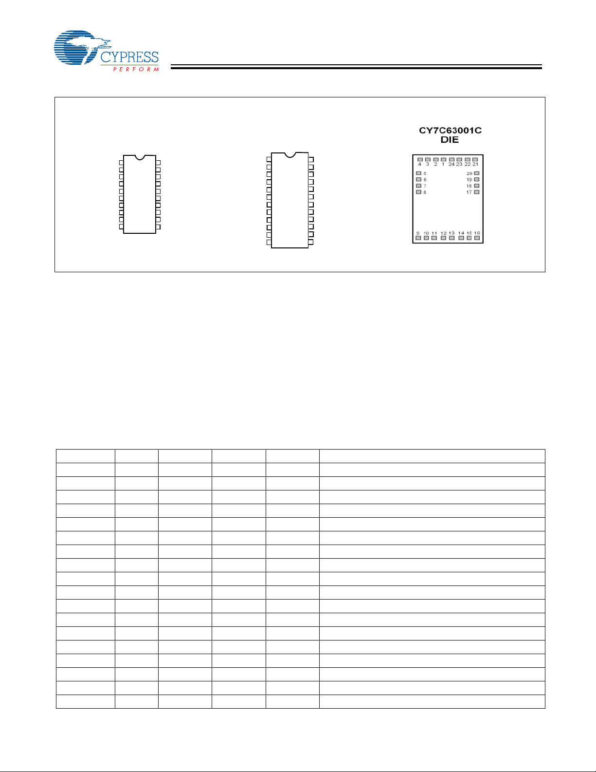
2.0 Pin Configurations
(Top View)
CY7C63001C
CY7C63101C
24-pin
SOIC/QSOP
P0.0
1
P0.1
2
P0.2
3
P0.3
4
P1.0
5
P1.2
6
P1.4
7
P1.6
8
V
9
SS
V
10
PP
11
12
P0.0
P0.1
P0.2
P0.3
P1.0
P1.2
V
V
CEXT
XTALIN
20-pin
DIP/SOIC
1
2
3
4
5
6
7
SS
8
PP
9
10
20
19
18
17
16
15
14
13
12
11
P0.4
P0.5
P0.6
P0.7
P1.1
P1.3
D+
D–
V
CC
XTALOUT
CEXT
XTALIN
3.0 Functional Overview
The CY7C630/101C is a family of 8-bit RISC One Time
Programmable (OTP) microcontrollers with a built-in 1.5-Mbps
USB Serial Interface Engine (SIE). The microcontroller
features 35 instructions that are optimized for USB applications. In addition, the microcontroller features 128 bytes of
internal RAM and 4 Kbytes of program memory space. The
Cypress USB Controller accepts a 6-MHz ceramic resonator
as its clock source. This clock signal is doubled within the chip
to provide a 12- MHz clock for the microprocessor.
The microcontroller features two ports of up to sixteen general
purpose I/Os (GPIOs). Each GPIO pin can be used to
generate an interrupt to the microcontroller. Additionally, all
P0.4
24
23
P0.5
P0.6
22
21
P0.7
P1.1
20
P1.3
19
18
P1.5
17
P1.7
16
D+
D–
15
V
14
CC
XTALOUT
13
pins in Port 1 are equipped with programmable drivers strong
enough to drive LEDs. The GPIO ports feature low EMI
emissions as a result of controlled rise and fall times and
unique output driver circuits. The Cypress microcontrollers
have a range of GPIOs to fit various applications; the
CY7C63001C has twelve GPIOs and the CY7C63101C has
sixteen GPIOs. Notice that each part has eight ‘low-current’
ports (Port 0) with the remaining ports (Port 1) being
‘high-current’ ports.
The 12-GPIO CY7C63001C is available in 20-pin PDIP (-PXC)
and 20-pin SOIC (-SXC) packages. The 16-GPIO
CY7C63101C is available in 24-pin QSOP (-QXC) package.
4.0 Pin Definitions
Name I/O 20-Pin 24-pin Die Pad # Description
P0.0 I/O 1 1 1 Port 0 bit 0
P0.1 I/O 2 2 2 Port 0 bit 1
P0.2 I/O 3 3 3 Port 0 bit 2
P0.3 I/O 4 4 4 Port 0 bit 3
P0.4 I/O 20 24 24 Port 0 bit 4
P0.5 I/O 19 23 23 Port 0 bit 5
P0.6 I/O 18 22 22 Port 0 bit 6
P0.7 I/O 17 21 21 Port 0 bit 7
P1.0 I/O 5 5 5 Port 1 bit 0
P1.1 I/O 16 20 20 Port 1 bit 1
P1.2 I/O 6 6 6 Port 1 bit 2
P1.3 I/O 15 19 19 Port 1 bit 3
P1.4 I/O – 7 7 Port 1 bit 4
P1.5 I/O – 18 18 Port 1 bit 5
P1.6 I/O – 8 8 Port 1 bit 6
P1.7 I/O – 17 17 Port 1 bit 7
XTALIN I 10 12 12 Ceramic resonator in
XTALOUT O 11 13 13 Ceramic resonator out
Document #: 38-08026 Rev. *B Page 2 of 28
Page 3
CY7C63001C
CY7C63101C
4.0 Pin Definitions (continued)
Name I/O 20-Pin 24-pin Die Pad # Description
CEXT I/O 9 11 11 Connects to external R/C timing circuit for optional
D+ I/O141616USB data+
D– I/O131515USB data–
V
PP
V
CC
V
SS
– 8 10 10 Programming voltage supply, tie to ground during normal
– 12 14 14 Voltage supply
–799Ground
5.0 Pin Description
Name Description
V
CC
V
SS
V
PP
XTALIN 1 pin. Input from an external ceramic resonator.
XT ALOUT 1 pin. Return path for the ceramic resonator (leave unconnected if driving XTALIN from an external oscillator).
P0.0–P0.7,
P1.0–P1.7
D+, D– 2 pins. Bidirectional USB data lines. An external pull-up resistor must be connected between the D pin and
CEXT 1 pin. Open-drain output with Schmitt trigger input. The input is connected to a rising edge-triggered interrupt.
1 pin. Connects to the USB power source or to a nominal 5V power supply. Actual VCC range can vary
between 4.0V and 5.25V.
1 pin. Connects to ground.
1 pin. Used in programming the on-chip EPROM. This pin should be tied to ground during normal operations.
16 pins. P0.0–P0.7 are the 8 I/O lines in Port 0. P1.0–P1.7 are the 8 I/O lines in Port 1. P1.0–P1.3 are
supported in the CY7C63001C. All I/O pins include bit-programmable pull-up resistors. However, the sink
current of each pin can be programmed to one of sixteen levels. Besides functioning as GPIO lines, each
pin can be programmed as an interrupt input. The interrupt is edge-triggered, with programmable polarity.
V
to select low-speed USB operation.
CC
CEXT may be connected to an external RC to generate a wake-up from Suspend mode. See Section 6.4.
‘suspend’ wakeup
operation
6.0 Functional Description
The Cypress CY7C630/101C USB microcontrollers are
optimized for human-interface computer peripherals such as
a mouse, joystick, and gamepad. These USB microcontrollers
conform to the low-speed (1.5 Mbps) requirements of the USB
specification version 1.1. Each microcontroller is a
self-contained unit with: a USB interface engine, USB transceivers, an 8-bit RISC microcontroller, a clock oscillator,
timers, and program memory. Each microcontroller supports
one USB device address and two endpoints.
The 6-MHz clock is doubled to 12 MHz to drive the microcontroller. A RISC architecture with 35 instructions provides the
best balance between performance and product cost.
6.1 Memory Organization
The memory in the USB Controller is organized into user
program memory in EPROM space and data memory in SRAM
space.
6.1.1 Program Memory Organization
The CY7C63001C and CY7C63101C each offer 4 Kbytes of
EPROM. The program memory space is divided into two
functional groups: interrupt vectors and program code.
The interrupt vectors occupy the first 16 bytes of the program
space. Each vector is 2 bytes long. After a reset, the Program
Counter points to location zero of the program space.
Figure 6-1 shows the organization of the Program Memory
Space.
6.1.2 Securi ty Fu se Bit
The Cypress USB microcontroller includes a security fuse bit.
When the security fuse is programmed, the EPROM program
memory outputs 0xFF to the EPROM programmer, thus
protecting the user’s code.
Document #: 38-08026 Rev. *B Page 3 of 28
Page 4

after reset Address
PC 0x0000 Reset Vector
0x0002 Interrupt Vector - 128 µs
0x0004 Interrupt Vector - 1.024 ms
0x0006 Interrupt Vector - USB Endpoint 0
0x0008 Interrupt Vector - USB Endpoint 1
0x000A Reserved
0x000C Interrupt Vector - GPIO
0x000E Interrupt Vector - Cext
0x0010 On-chip program Memory
CY7C63001C
CY7C63101C
0x0FFF 4K ROM
Figure 6-1. Program Memory Space
Document #: 38-08026 Rev. *B Page 4 of 28
Page 5
CY7C63001C
CY7C63101C
6.1.3 Data Memory Organization
The USB Controller includes 128 bytes of data RAM. The
upper 16 bytes of the data memory are used as USB FIFOs
for Endpoint 0 and Endpoint 1. Each endpoint is associated
with an 8-byte FIFO.
The USB controller includes two pointers into data RAM, the
Program Stack Pointer (PSP) and the Data Stack Pointer
(DSP). The value of PSP after reset is 0x00. The PSP increments by 2 whenever a CALL instruction is executed and it
decrements by 2 whenever a RET instruction is used.
after reset
DSP PSP
user
firmware
DSP
The DSP pre-decrements by 1 whenever a PUSH instruction
is executed and it increments by 1 after a POP instruction is
used. The default value of the DSP after reset is 0x00, which
would cause the first PUSH to write into USB FIFO space for
Endpoint 1. Therefore, the DSP should be mapped to a
location such as 0x70 before initiating any data stack operations. Refer to the Reset section for more information about
DSP remapping after reset. Figure 6-2 illustrates the Data
Memory Space.
Address
0x00
0x02
0x04
0x70 USB FIFO - Endpoint 0
0x77
0x78 USB FIFO - Endpoint 1
0x7F
Figure 6-2. Data Memory Space
Document #: 38-08026 Rev. *B Page 5 of 28
Page 6

CY7C63001C
CY7C63101C
6.2 I/O Register Summary
I/O registers are accessed via the I/O Read (IORD) and I/O
Write (IOWR, IOWX) instructions.
Table 6-1. I/O Register Summary
Register Name I/O Address Read/Write Function Page
P0 Data 0x00 R/W General purpose I/O Port (low current) 9
P1 Data 0x01 R/W General purpose I/O Port (high current) 9
P0 IE 0x04 W Interrupt enable for Port 0 pins 12
P1 IE 0x05 W Interrupt enable for Port 1 pins 12
P0 Pull-up 0x08 W Pull-up resistor control for Port 0 pins 10
P1 Pull-up 0x09 W Pull-up resistor control for Port 1 pins 10
EP0 TX Config. 0x10 R/W USB Endpoint 0 transmit configuration 15
EP1 TX Config. 0x11 R/W USB Endpoint 1 transmit configuration 15
USB DA 0x12 R/W USB device address 14
USB SCR 0x13 R/W USB status and control 16
EP0 RX Status 0x14 R/W USB Endpoint 0 receive status 14
GIE 0x20 R/W Global Interrupt Enable 11
WDT 0x21 W Watch Dog Timer clear 7
Cext 0x22 R/W External R-C Timing circuit control 8
Timer 0x23 R Free-running timer 8
P0 Isink 0x30-0x37 W Input sink current control for Port 0 pins. There is
P1 Isink 0x38-0x3F W Input sink current control for Port 1 pins. There is
SCR 0xFF R/W Processor status and control register 7
one Isink register for each pin. Address of the Isink
register for pin 0 is located at 0x30 and the register
address for pin 7 is located at 0x37.
one Isink register for each pin. Address of the Isink
register for pin 0 is located at 0x38 and the register
address for pin 7 is located at 0x3F. The number
of Port 1 pins depends on package type.
10
10
6.3 Reset
The USB Controller supports three types of resets. All
registers are restored to their default states during a reset. The
USB Device Address is set to 0 and all interrupts are disabled.
In addition, the Program Stack Pointer (PSP) is set to 0x00 and
the Data Stack Pointer (DSP) is set to 0x00. The user should
set the DSP to a location such as 0x70 to reserve 16 bytes of
USB FIFO space. The assembly instructions to do so are:
MOV A, 70h ; Move 70 hex into Accumulator, use 70
instead of 6F because the dsp is
; always decremented by 1 before the
data transfer of the PUSH instruction occurs
SWAP A, DSP ; Move Accumulator value into dsp
The three reset types are:
1. Power-On Reset (POR)
2. Watch Dog Reset (WDR)
3. USB Reset
The occurrence of a reset is recorded in the Status and Control
Register located at I/O address 0xFF (Figure 6-3). Reading
Document #: 38-08026 Rev. *B Page 6 of 28
and writing this register are supported by the IORD and IOWR
instructions. Bits 1, 2, and 7 are reserved and must be written
as zeros during a write. During a read, reserved bit position s
should be ignored. Bits 4, 5, and 6 are used to record the
occurrence of POR, USB, and WDR Reset respectively. The
firmware can interrogate these bits to determine the cause of
a reset. If a Watch Dog Reset occurs, firmware must clear the
WDR bit (bit 6) in the Status and Control Register to re-enable
the USB transmitter (please refer to the Watch Dog Reset
section for further details). Bit 0, the “Run” control, is set to 1
at POR. Clearing this bit stops the microcontroller (firmware
normally should not clear this bit). Once this bit is set to LOW,
only a reset can set this bit HIGH.
The microcontroller resumes execution from ROM address
0x00 after a reset unless the Suspend bit (bit 3) of the Status
and Control Register is set. Setting the Suspend bit stops the
clock oscillator and the interrupt timers and powers down the
microcontroller. The detection of any USB activity, the occurrence of a GPIO Interrupt, or the occurrence of the Cext
Interrupt terminates the suspend condition.
Page 7
CY7C63001C
CY7C63101C
b7 b6 b5 b4 b3 b2 b1 b0
Reserved WDR USBR POR SUSPEND Reserved Reserved RUN
R/W R/W R/W R/W R/W
0 0 0 1 0 0 0 1
Figure 6-3. Status and Control Register (SCR - Address 0xFF)
6.3.1 Power-On Reset (POR)
Power-On Reset (POR) occurs every time the power to the
device is switched on. Bit 4 of the Status and Control Register
is set to record this event (the register contents are set to
00011001 by the POR). The USB Controller is placed in
suspended mode at the end of POR to conserve power (the
clock oscillator, the timers, and the interrupt logic are turned
off in suspend mode). After POR, only a non-idle USB Bus
state terminates the suspend mode. The microcontroller then
begins execution from ROM address 0x00.
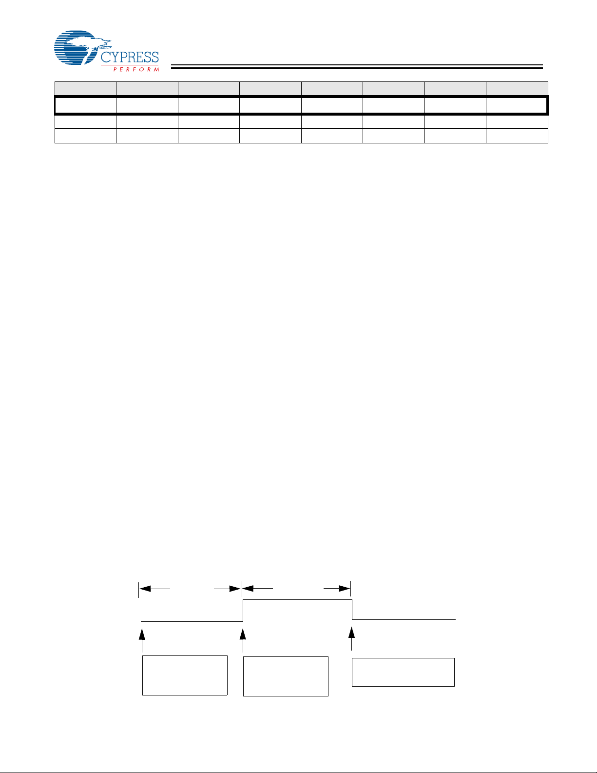
6.3.2 Watch Dog Reset (WDR)
The Watch Dog Timer Reset (WDR) occurs when the Most
Significant Bit of the 4-bit Watch Dog Timer Register transitions from LOW to HIGH. Writing any value to the write-only
Watch Dog Rest art Register at 0x21 clears the tim er (firmware
should periodically write to the Watch Dog Restart Register in
the ‘main loop’ of firmware). The Watch Dog timer is clocked
by a 1.024-ms clock from the free-running timer. If 8 clocks
occur between writes to the timer, a WDR occurs and bit 6 of
the Status and Control Register is set to record the event. A
Watch Dog Timer Reset lasts for 8.192 ms, at which time the
microcontroller begins execution at ROM address 0x00. The
USB transmitter is disabled by a Watch Dog Reset because
the USB Device Address Register is cleared (otherwise, the
USB Controller would respond to all address 0 transactions).
The transmitter remains disabled until the WDR bit (bit 6) in
the Status and Control Register is reset to 0 by firmware.
6.3.3 USB Bus Reset
The USB Controller recognizes a USB Reset when a Sin gle
Ended Zero (SE0) condition persists for at least 8–16 µs (the
Reset may be recognized for an SE0 as short as 8 µs, but it is
always recognized for an SE0 longer than 16 µs). SE0 is the
condition in which both the D+ line and the D– line are LOW.
Bit 5 of the Status and Control Register is set to record this
event. If the USB reset happens while the device is
suspended, the suspend condition is cleared and the clock
oscillator is restarted. However, the microcontroller is not
released until the USB reset is removed.
6.4 Instant-on Feature (Suspend Mode)
The USB Controller can be placed in a low-power state by
setting the Suspend bit (bit 3) of the Status and Control
register. All logic blocks in the device are turned off except the
USB receiver, the GPIO interrupt logic, and the Cext interrupt
logic. The clock oscillator and the free-running and watch dog
timers are shut down.
The suspend mode is terminated when one of the following
three conditions occur:
1. USB activity
2. A GPIO interrupt
3. Cext interrupt
The clock oscillator, GPIO, and timers restart immediately
upon exiting suspend mode. The USB engine and microcontroller return to a fully functional state no more than 256 µs
later. Before servicing any interrupt requests, the microcontroller executes the instruction following the I/O write that
placed the device into suspend mode.
Both the GPIO interrupt and the Cext interrupt allow the USB
Controller to wake-up periodically and poll potentiometers,
optics, and other system components while maintaining a very
low average power consumption. The Cext Interrupt is
preferred for lowest power consumption.
For Cext to generate an “Instant-on” interrupt, the pin must be
connected to ground with an external capacitor and connected
to V
with an external resistor. A “0” is written to the Cext
CC
register located at I/O address 0x22 to discharge the capacitor.
Then, a “1” is written to disable the open-drain output driver. A
Schmitt trigger input circuit monitors the input and generates
a wake-up interrupt when the input voltage rises above the
input threshold. By changing the values of the external resistor
and capacitor, the user can fine tune the charge rate of the R-C
timing circuit. The format of the Cext register is shown in
7.168 to
8.192 ms
Last write to
Watchdog Timer
Register
Document #: 38-08026 Rev. *B Page 7 of 28
No write to WDT
register, so WDR
goes HIGH
Figure 1. Watch Dog Reset (WDR)
8.192 ms
Execution begins at
Reset Vector 0x00
Page 8
CY7C63001C
CY7C63101C
Figure 6-4. Reading the register returns the value of the Cext
pin. During a reset, the Cext pin is HIGH.
b7 b6 b5 b4 b3 b2 b1 b0
Reserved Reserved Reserved Reserved Reserved Reserved Reserved CEXT
0 0 0 0 0 0 0 1
Figure 6-4. The Cext Register (Address 0x22)
R/W
6.5 On-Chip Timer
The USB Controller is equipped with a free-running timer
driven by a clock one-sixth the resonator frequency. Bits 0
through 7 of the counter are readable from the read-only Timer
Register located at I/O address 0x23. The Timer Register is
cleared during a Power-On Reset and whenever Suspend
b7 b6 b5 b4 b3 b2 b1 b0
T.7 T.6 T.5 T.4 T.3 T.2 T.1 T.0
R R R R R R R R
0 0 0 0 0 0 0 0
Figure 6-5. Timer Register (Address 0x23)
mode is entered. Figure 6-5 illustrates the format of this
register and Figure 6-6 is its block diagram.
With a 6 MHz resonator, the timer resolution is 1 µs.
The timer generates two interrupts: the 128-µs interrupt and
the 1.024-ms interrupt.
1.024-ms interrupt
µs interrupt
128-
9
8
7
6
5
4
3
2
1
0
Resonator Clock/6
8
To Timer Register
Figure 6-6. Timer Block Diagram
Document #: 38-08026 Rev. *B Page 8 of 28
Page 9
CY7C63001C
CY7C63101C
6.6 General Purpose I/O Ports
Interface with peripherals is conducted via as many as 16
GPIO signals. These signals are divided into two ports: Port 0
and Port 1. Port 0 contains eight lines (P0.0–P0.7) and Port 1
contains up to eight lines (P1.0–P1.7). The number of external
I/O pins depends on the package type. Both ports can be
accessed by the IORD, IOWR, and IOWX instructions. The
Port 0 data register is located at I/O address 0x00 while the
Port 1 data register is located at I/O address 0x01. The
contents of both registers are set HIGH during a reset. Refer
to Figures 6-7 and 6-8 for the formats of the data registers. In
addition to supporting general input/output functions, each I/O
line can trigger an interrupt to the microcontroller. Please refer
to the interrupt section for more details.
Each GPIO line includes an internal R
provides both the pull-up function and slew control. Two
factors govern the enabling and disabling of each resistor: the
state of its associated Port Pull-up register bit and the state of
the Data Register bit. NOTE: The control bits in the Port
Pull-up register are active LOW.
b7 b6 b5 b4 b3 b2 b1 b0
P0.7 P0.6 P0.5 P0.4 P0.3 P0.2 P0.1 P0.0
R/W R/W R/W R/W R/W R/W R/W R/W
1 1 1 1 1 1 1 1
resistor. This resistor
up
Figure 6-7. Port 0 Data Register (Address 0x00)
A GPIO line is HIGH when a “1” is written to the Data Register
and a “0” is written to the respective Port Pull-up register.
Writing a “0” to the port Data Register disables the port’s
Pull-up resistor and outputs a LOW on the GPIO line
regardless of the setting in the Port Pull-up Register. The
output goes to a high-Z state if the Data Register bit and the
Port Pull-up Register bit are both “1”. Figure 6-9 illustrates the
block diagram of one I/O line. The Port Isink Register is used
to control the output current level and it is described later in
this section. NOTE: The Isink logic block is turned off during
suspend mode (please refer to the Instant-on Feature section
for more details). Therefore, to prevent higher I
during USB suspend mode, firmware must set ALL Port 0 and
Port 1 Data Register bits (which are not externally driven to a
known state), including those that are not bonded out on a
particular package, to “1” and all Port 0 and Port 1 Pull-Up
Register data bits to “0” to enable port pull-ups before setting
the Suspend bit (bit 3 of the Status and Control Register).
Table 6-2 is the Output Control truth table.
currents
CC
b7 b6 b5 b4 b3 b2 b1 b0
P1.7 P1.6 P1.5 P1.4 P1.3 P1.2 P1.1 P1.0
R/W R/W R/W R/W R/W R/W R/W R/W
1 1 1 1 1 1 1 1
Figure 6-8. Port 1 Data Register (Address 0x01)
V
CC
Port Pull-Up
Register
R
Port Data
Register
Port Isink
Register
Suspend
Bit
Data Bus
Isink
DAC
Disable
Schmitt
Trigger
up
GPIO
Pin
Figure 6-9. Block Diagram of an I/O Line
Document #: 38-08026 Rev. *B Page 9 of 28
Page 10

Table 6-2. Output Control Truth Table
Data Register Port Pull-up Register Output at I/O Pin Interrupt Polarity
0 0 Sink Current (‘0’) High to Low
0 1 Sink Current (‘0’) Low to High
1 0 Pull-up Resistor (‘1’) High to Low
1 1 Hi-Z Low to High
CY7C63001C
CY7C63101C
To configure a GPIO pin as an input, a “1” should be written to
the Port Data Register bit associated with that pin to disable
the pull-down function of the Isink DAC (see Figure 6-9).When
the Port Data Register is read, the bit value is a “1” if the
voltage on the pin is greater than the Schmitt trigger threshold,
or “0” if it is below the threshold. In applications where an
internal pull-up is required, the R
engaged by writing a “0” to the appropriate bit in the Port
Pull-up Register.
Both Port 0 and Port 1 Pull-up Registers are write only (see
Figures 6-10 and 6-11). The Port 0 Pull-up Register is located
at I/O address 0x08 and Port 1 Pull-up Register is mapped to
address 0x09. The contents of the Port Pull-up Registers are
cleared during reset, allowing the outputs to be controlled by
the state of the Data R egisters. The Port Pull-up Registers also
select the polarity of transition that generates a GPIO interrupt.
A “0” selects a HIGH to LOW transition while a “1” selects a
LOW to HIGH transition.
b7 b6 b5 b4 b3 b2 b1 b0
PULL0.7 PULL0.6 PULL0.5 PULL0.4 PULL0.3 PULL0.2 PULL0.1 PULL0.0
W W W W W W W W
0 0 0 0 0 0 0 0
pull-up resistor can be
up
Figure 6-10. Port 0 Pull-up Register (Address 0x08)
Writing a “0” to the Data Register drives the output LOW.
Instead of providing a fixed output drive, the USB Controller
allows the user to select an output sink current level for each
I/O pin. The sink current of each output is controlled by a
dedicated Port Isink Register. The lower four bits of this
register contain a code selecting one of sixteen sink current
levels. The upper four bits of the register are ignored. The
format of the Port Isink Register is shown in Figure 6-12.
Port 0 is a low-current port suitable for connecting photo
transistors. Port 1 is a high current port capable of driving
LEDs. See section 8.0 for current ranges. 0000 is the lowest
drive strength. 1111 is the highest.
The write-only sink current control registers for Port 0 outputs
are assigned from I/O address 0x30 to 0x37 with the control
bits for P00 starting at 0x30. Port 1 sink current control
registers are assigned from I/O address 0x38 to 0x3F with the
control bits for P10 starting at 0x38. All sink current control
registers are cleared during a reset, resulting in the minimum
current sink setting.
b7 b6 b5 b4 b3 b2 b1 b0
PULL1.7 PULL1.6 PULL1.5 PULL1.4 PULL1.3 PULL1.2 PULL1.1 PULL1.0
W W W W W W W W
0x 0 0 0 0 0 0 0
Figure 6-1 1 . Por t 1 Pul l-up Register (Address 0x09)
b7 b6 b5 b4 b3 b2 b1 b0
Reserved Reserved Reserved UNUSED ISINK3 ISINK2 ISINK1 ISINK0
W W W W W W W W
x x x x x x x x
Figure 6-12. Port Isink Register for One GPIO Line
Document #: 38-08026 Rev. *B Page 10 of 28
Page 11

CY7C63001C
CY7C63101C
XTALOUT
clk1x
(to USB SIE)
clk2x
(to Microcontroller)
6.7 XTALIN/XTALOUT
The XTALIN and XTALOUT pins support connection of a
6-MHz ceramic resonator. The feedback capacitors and bias
resistor are internal to the IC, as shown in Figure 2 Leave
XTALOUT unconnected when driving XT ALIN from an external
oscillator.
6.8 Interrupts
Interrupts are generated by the General Purpose I/O lines, the
Cext pin, the internal timer, and the USB engine. All interrupts
are maskable by the Global Interrupt Enable Register. Access
to this register is accomplished via IORD, IOWR, and IOWX
instructions to address 0x20. Writing a “1” to a bit position
enables the interrupt associated with that position. Du ring a
reset, the contents of the Interrupt Enable Register are
cleared, disabling all interrupts. Figure 6-13 illustrates the
format of the Global Interrupt Enable Register.
b7 b6 b5 b4 b3 b2 b1 b0
CEXTIE GPIOIE Reserved EP1IE EP0IE 1024IE 128IE Reserved
R/W R/W R/W R/W R/W R/W
0 0 0 0 0 0 0 0
Figure 6-13. Global Interrupt Enable Register (GIER - Address 0x20)
Clock
Doubler
Figure 2. Clock Oscillator On-chip Circuit
The interrupt controller contains a separate latch for each
interrupt. See Figure 3 for the logic block diagram for the
interrupt controller. When an interrupt is generated, it is
latched as a pending interrupt. It stays as a pending interrupt
until it is serviced or a reset occurs. A pending interrupt only
generates an interrupt request if it is enabled in the Global
Interrupt Enable Register. The highest priority interrupt
request is serviced following the execution of the current
instruction.
When servicing an interrupt, the hardware first disables all
interrupts by clearing the Global Interrupt Enable Register.
Next, the interrupt latch of the current interrupt is cleared. This
is followed by a CALL instruction to the ROM address
associated with the interrupt being serviced (i.e., the interrupt
vector). The instruction in the interrupt table is typically a JMP
instruction to the address of the Interrupt Service Routine
(ISR). The user can re-enable interrupts in the interrupt service
routine by writing to the appropriate bits in the Global Interrupt
Enable Register. Interrupts can be nested to a level limited
only by the available stack space.
XTALIN
30 pF30 pF
128-
µ
s CLR
CLR
µ
s
DQ
CLK
CLR
DQ
CLK
CLR
DQ
CLK
Enable [1]
Enable [6]
Enable [7]
128-µs IRQ
1-ms CLR
1-ms IRQ
End P0 CLR
End P0 IRQ
End P1 CLR
End P1 IRQ
GPIO CLR
GPIO IRQ
Wake-up CLR
Wake-up IRQ
Interrupt
Priority
Encoder
IRQ
Interrupt
Vector
Global
Interrupt
Enable
Register
CLR
Interrupt
Acknowledge
Logic 1
128-
Interrupt
Enable [7:0]
Logic 1
GPIO
Interrupt
Logic 1
CEXT
Figure 3. Interrupt Controller Logic Block Diagram
Document #: 38-08026 Rev. *B Page 11 of 28
Page 12

CY7C63001C
CY7C63101C
The Program Counter (PC) value and the Carry and Zero flags
(CF, ZF) are automatically stored onto the Program Stack by
the CALL instruction as part of the interrupt acknowledge
process. The user firmware is responsible for ensuring that the
processor state is preserved and restored during an interrupt.
For example the PUSH A instruction should be used as the
first command in the ISR to save the accumulator value. And,
the IPRET instruction should be used to exit the ISR with the
accumulator value restored and interrupts enabled. The PC,
CF, and ZF are restored when the IPRET or RET instructions
are executed.
The Interrupt Vectors supported by the USB Controller are
listed in Table 6-3. Interrupt Vector 0 (Reset) has the highest
priority, Interrupt Vector 7 has the lowest priority. Because the
JMP instruction is 2 bytes long, the interrupt vectors occupy 2
bytes.
6.8.1 Interrupt Latency
Interrupt latency can be calculated from the following
equation:
Interrupt Latency = (Number of clock cycles remaining in the
current instruction) + (10 clock cycles for
the CALL instruction) + (5 clock cycles
for the JMP instruction)
For example, if a 5-clock-cycle instruction such as JC is being
executed when an interrupt occurs, the first instruction of the
Interrupt Service Routine executes a minimum of 16 clock
cycles (1+10+5) or a maximum of 20 clock cycles (5+10+5)
after the interrupt is issued . Th e r e fo re, the interrupt latency in
this example will be = 20 clock periods = 20 / (12 MHz) =
1.667 µs. The interrupt latches are sampled at the rising edge
of the last clock cycle in the current instruction.
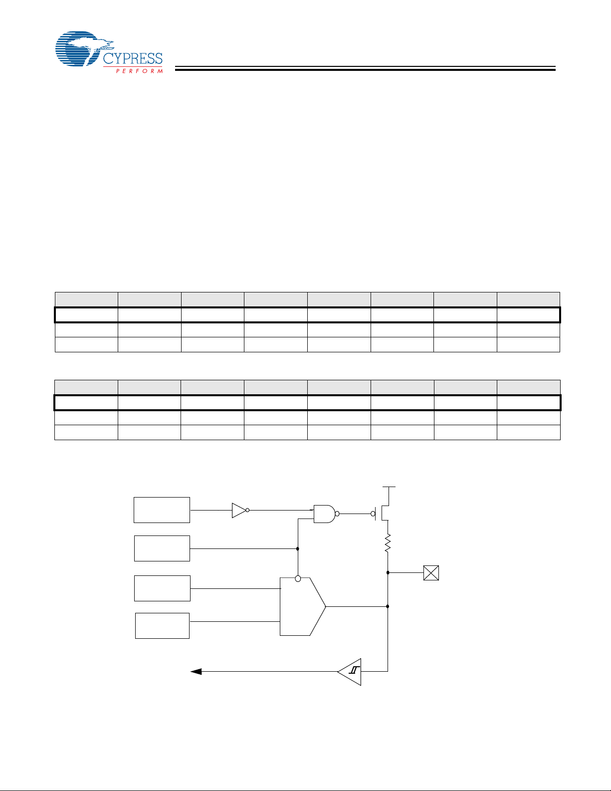
6.8.2 GPIO Interrupt
The General Purpose I/O interrupts are generated by signal
transitions at the Port 0 and Port 1 I/O pins. GPIO interrupts
are edge sensitive with programmable interrupt polarities.
Setting a bit HIGH in the Port Pull-up Register (see
Figure 6-10 and 6-11) select s a LOW to HIGH interrupt trigger
for the corresponding port pin. Setting a bit LOW activates a
HIGH to LOW interrupt trigger. Each GPIO interrupt is
maskable on a per-pin basis by a dedicated bit in the Port
Interrupt Enable Register. Writing a “1” enables the interrupt.
Figure 6-14 and Figure 6-15 illustrate the format of the Port
Interrupt Enable Registers for Port 0 and Port 1 located at I/O
address 0x04 and 0x05 respectively. These write only
registers are cleared during reset, thus disabling all GPIO
interrupts.
A block diagram of the GPIO interrupt logic is shown in
Figure 6-16. The bit setting in the Port Pull-up Register selects
the interrupt polarity. If the selected signal polarity is detected
on the I/O pin, a HIGH signal is generated. If the Port Interrupt
Enable bit for this pin is HIGH and no other port pins are
requesting interrupts, the OR gate issues a LOW to HIGH
signal to clock the GPIO interrupt flip-flop. The output of the
flip-flop is further qualified by the Global GPIO Interrupt Enable
bit before it is processed by the Interrupt Priority Encoder. Both
the GPIO interrupt flip-flop and the Global GPIO Enable bit are
cleared by on-chip hardware during GPIO interrupt
acknowledge.
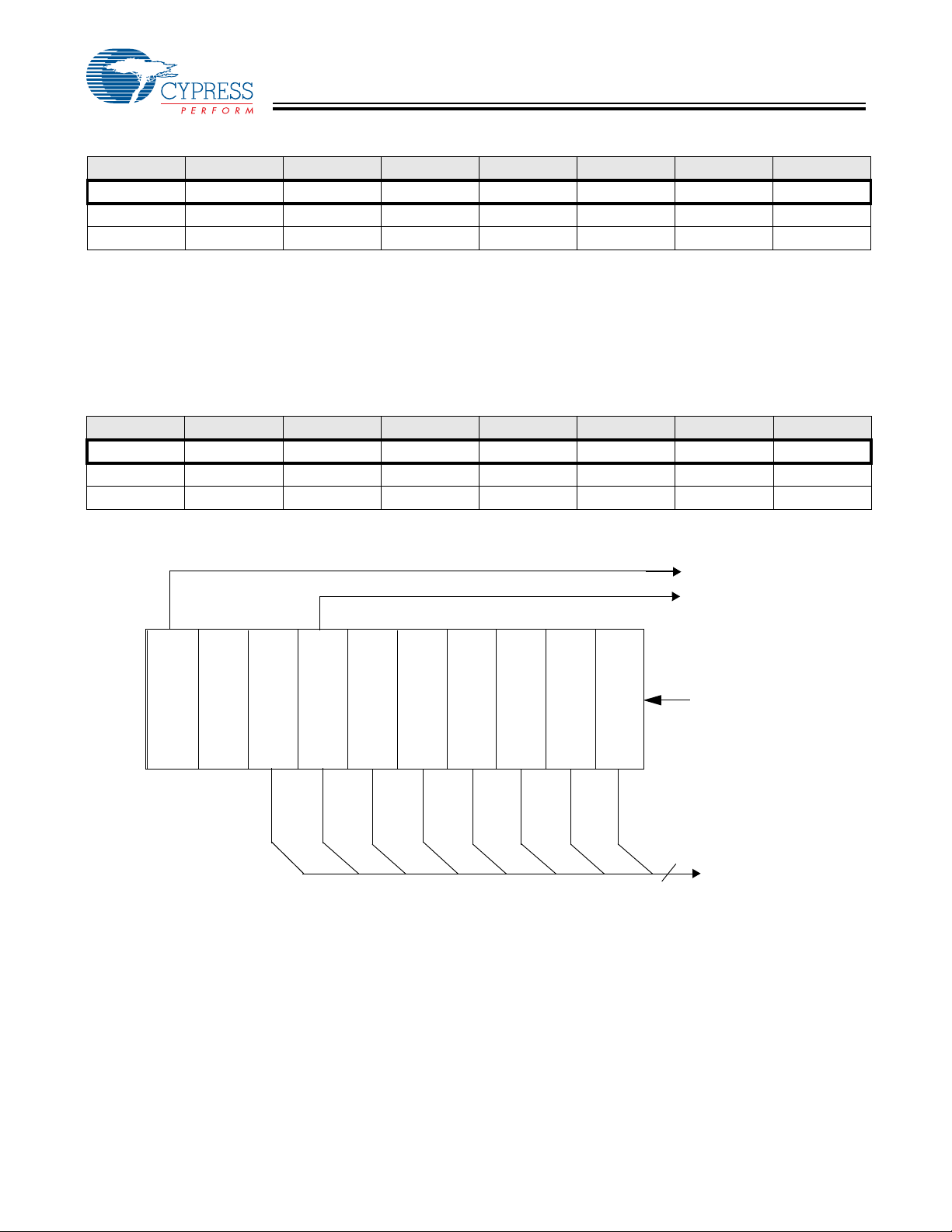
Table 6-3. Interrupt Vector Assignments
Interrupt Priority ROM Address Function
0 (Highest) 0x00 Reset
1 0x02 128-µs timer interrupt
2 0x04 1.024-ms timer interrupt
3 0x06 USB endpoint 0 interrupt
4 0x08 USB endpoint 1 interrupt
5 0x0A Reserved
6 0x0C GPIO interrupt
7 (Lowest) 0x0E Wake-up interrupt
b7 b6 b5 b4 b3 b2 b1 b0
IE0.7 IE0.6 IE0.5 IE0.4 IE0.3 IE0.2 IE0.1 IE0.0
W W W W W W W W
0 0 0 0 0 0 0 0
Figure 6-14. Port 0 Interrupt Enable Register (P0 IE - Address 0x04)
b7 b6 b5 b4 b3 b2 b1 b0
IE1.7 IE1.6 IE1.5 IE1.4 IE1.3 IE1.2 IE1.1 IE1.0
W W W W W W W W
0 0 0 0 0 0 0 0
Figure 6-15. Port 1 Interrupt Enable Register (P1 IE - Address 0x05)
Document #: 38-08026 Rev. *B Page 12 of 28
Page 13

CY7C63001C
CY7C63101C
GPIO
Pin
1 = Enable
0 = Disable
Interrupt
Acknowledge
Port
Pull-Up
Register
M
U
X
Port Interrupt
Enable Register
1 = Enable
0 = Disable
(Bit 6, Register 0x20)
→H
1=L
0=H
→L
CLR
Global
GPIO Interrupt
Enable
Figure 6-16. GPIO Interrupt Logic Block Diagram
Note: If one port pin triggers an interrupt, no other port pin can
cause a GPIO interrupt until the port pin that triggered the
interrupt has returned to its inactive (non-trigger) state or until
its corresponding port interrupt enable bit is cleared (these
events ‘reset’ the clock of the GPIO Interrupt flip-flop, which
must be ‘reset’ to ‘0’ before another GPIO interrupt event can
‘clock’ the GPIO Interrupt flip-flop and produce an IRQ).
Note: If the port pin that triggered an interrupt is held in its
active (trigger) state while its corresponding port interrupt
enable bit is cleared and then set, a GPIO interrupt event
occurs as the GPIO Interrupt flip-flop clock tran sition s from ‘1 ’
to ‘0’ and then back to ‘1’ (please refer to Figure 6-16). The
USB Controller does not assign interrupt priority to different
port pins and the Port Interrupt Enable Registers are not
cleared during the interrupt acknowledge process. When a
GPIO interrupt is serviced, the ISR must poll the ports to
determine which pin caused the interrupt.
6.8.3 USB Interrupt
A USB Endpoint 0 interrupt is generated after the host has
written data to Endpoint 0 or after the USB Controller has
transmitted a packet from Endpoint 0 and receives an ACK
from the host. An OUT packet from the host which is NAKed
by the USB Controller does not generate an interrupt. This
interrupt is masked by the USB EP0 Interrupt Enable bit (bit 3)
of the Global Interrupt Enable Register.
A USB Endpoint 1 interrupt is generated after the USB
Controller has transmitted a packet from Endpoint 1 and has
received an ACK from the host. This interrupt is masked by the
USB EP1 Interrupt Enable bit (bit 4) of the Global Interrupt
Enable Register.
6.8.4 Timer Interrupt
There are two timer interrupts: the 128-µs interrupt and the
1.024-ms interrupt. They are masked by bits 1 and 2 of the
Global Interrupt Enable Register respectively. The user should
disable both timer interrupts before going into the suspend
GPIO Interrupt
OR Gate
(1 input per
GPIO pin)
Flip-Flop
I
D
CLR
Q
Interrupt
Priority
Encoder
IRQ
Interrupt
Vector
mode to avoid possible conflicts from timer interrupts occurring
just as suspend mode is entered.
6.8.5 Wake-Up Interrupt
A wake-up interrupt is generated when the Cext pin goes
HIGH. This interrupt is latched in the interrupt controller. It can
be masked by the Wake-up Interrupt Enable bit (bit 7) of the
Global Interrupt Enable Register. This interrupt can be used to
perform periodic checks on attached peripherals when the
USB Controller is placed in the low-power suspend mode. See
the Instant-On Feature section for more details.
6.9 USB Engine
The USB engine includes the Serial Interface Engine (SIE)
and the low-speed USB I/O transceivers. The SIE block
performs most of the USB interface functions with only minimal
support from the microcontroller core. Two endpoints are
supported. Endpoint 0 is used to receive and transmit control
(including setup) packets while Endpoint 1 is only used to
transmit data packets.
The USB SIE processes USB bus activity at the transaction
level independently. It does all the NRZI encoding/decoding
and bit stuffing/unstuffing. It also determines token type,
checks address and endpoint values, generates and checks
CRC values, and controls the flow of data bytes between the
bus and the Endpoint FIFOs. NOTE: the SIE stalls the CPU for
3 cycles per byte when writing data to the endpoint FIFOs (or
3 * 1/12 MHz * 8 bytes = 2 µs per 8-byte transfer).
The firmware handles higher level and function-specific tasks.
During control transfers the firmware must interpret device
requests and respond correctly. It also must coordinate
Suspend/Resume, verify and select DATA toggle values, and
perform function specific tasks.
The USB engine and the firmware communicate though the
Endpoint FIFOs, USB Endpoint interrupts, and the USB
registers described in the sections below.
Document #: 38-08026 Rev. *B Page 13 of 28
Page 14

CY7C63001C
CY7C63101C
b7 b6 b5 b4 b3 b2 b1 b0
Reserved ADR6 ADR5 ADR4 ADR3 ADR2 ADR1 ADR0
R/W R/W R/W R/W R/W R/W R/W
0 0 0 0 0 0 0 0
Figure 6-17. USB Device Address Register (USB DA - Address 0x12)
6.9.1 USB Enumeration Process
The USB Controller provides a USB Device Address Register
at I/O location 0x12. Reading and writing this register is
achieved via the IORD and IOWR instructions. The register
contents are cleared during a reset, setting the USB address
of the USB Controller to 0. Figure 6-17 shows the format of the
USB Address Register.
Typical enumeration steps:
1. The host computer sends a SETUP packet followed by a
DATA packet to USB address 0 requesting the Device
descriptor.
2. The USB Controller decodes the request and retrieves its
Device descriptor from the program memory space.
3. The host computer performs a control read sequence and
the USB Controller responds by sending the Device
descriptor over the USB bus.
4. After receiving the descriptor, the host computer sends a
SETUP packet followed by a DATA packet to address 0
assigning a new USB address to the device.
5. The USB Controller stores the new address in its USB
Device Address Register after the no-data control
sequence completes.
6. The host sends a request for the Device descriptor using
the new USB address.
7. The USB Controller decodes the request and retrieves the
Device descriptor from the program memory.
8. The host performs a control read sequence and the USB
Controller responds by sending its Device descriptor over
the USB bus.
9. The host generates control reads to the USB Controller to
request the Configuration and Report descriptors.
10.The USB Controller retrieves the descriptors from its
program space and returns the data to the host over the
USB.
1 1.Enumeration is complete after the host has received all the
descriptors.
6.9.2 Endpoint 0
All USB devices are required to have an endpoint number 0
that is used to initialize and manipulate the device. Endpoint 0
provides access to the device’s configuration information and
allows generic USB status and control accesses.
Endpoint 0 can receive and transmit data. Both receive and
transmit data share the same 8-byte Endpoint 0 FIFO located
at data memory space 0x70 to 0x77. Received data may
overwrite the data previously in the FIFO.
6.9.2.1 Endpoint 0 Receive
After receiving a packet and placing the data into the Endpoint
0 FIFO, the USB Controller updates the USB Endpoint 0 RX
register to record the receive status and then generates a USB
Endpoint 0 interrupt. The format of the Endpoint 0 RX Register
is shown in Figure 6-18.
This is a read/write register located at I/O addre ss 0x14. An y
write to this register clears all bits except bit 3 which remains
unchanged. All bits are cleared during reset.
Bit 0 is set to 1 when a SETUP token for Endpoint 0 is received.
Once set to a 1, this bit remains HIGH until it is cleared by an
I/O write or a reset. While the data following a SETUP is being
received by the USB engine, this bit is not cleared by an I/O
write. User firmware writes to the USB FIFOs are disabled
when bit 0 is set. This prevents SETUP data from being
overwritten.
Bits 1 and 2 are updated whenever a valid token is received
on Endpoint 0. Bit 1 is set to 1 if an OUT token is received and
cleared to 0 if any other token is received. Bit 2 is set to 1 if an
IN token is received and cleared to 0 if any other token is
received.
Bit 3 shows the Data Toggle status of DATA packets received
on Endpoint 0. This bit is updated for DATA following SETUP
tokens and for DATA following OUT tokens if Stall (bit 5 of
0x10) is not set and either EnableOuts or StatusOuts (bits 3
and 4 of 0x13) are set.
Bits 4 to 7 are the count of the number of bytes received in a
DATA packet. The two CRC bytes are included in the count,
so the count value is two greater than the number of data bytes
received. The count is always updated and the data is always
stored in the FIFO for DAT A p ackets following a SETUP token.
The count for DATA following an OUT token is updated if Stall
(bit 5 of 0x10) is 0 and either EnableOuts or StatusOuts (bits
3 and 4 of 0x13) are 1. The DATA following an OUT is written
into the FIFO if EnableOuts is set to 1 and Stall and St atusOuts
are 0.
b7 b6 b5 b4 b3 b2 b1 b0
COUNT3 COUNT2 COUNT1 COUNT0 TOGGLE IN OUT SETUP
R/W R/W R/W R/W R R/W R/W R/W
0 0 0 0 0 0 0 0
Figure 6-18. USB Endpoint 0 RX Register (Address 0x14)
Document #: 38-08026 Rev. *B Page 14 of 28
Page 15

CY7C63001C
CY7C63101C
A maximum of 8 bytes are writte n into the Endpoint 0 FIFO. If
there are less than 8 bytes of data the CRC is written into the
FIFO.
Due to register space limitations, the Receive Data Invalid bit
is located in the USB Endpoint 0 TX Configuration Register.
Refer to the Endpoint 0 Transmit section for details. This bit is
set by the SIE if an error is detected in a received DA T A packet.
Table 6-4 summarizes the USB Engine response to SETUP
and OUT transactions on Endpoint 0. In the Data Packet
column ‘Error’ represents a packet with a CRC, PID or
bit-stuffing error, or a packet with more than 8 bytes of data.
‘Valid’ is a packet without an Error. ‘Status’ is a packet that is
a valid control read Status stage, while ‘N/Status’ is not a
correct Status stage (see section 6.9.4). The ‘Stall’ bit is
described in Section 6.9.2.2. The ‘StatusOuts’ and
‘EnableOuts’ bits are described in section 6.9.4.
6.9.2.2 Endpoint 0 Transmit
The USB Endpoint 0 TX Register located at I/O address 0x10
controls data transmission from Endpoint 0 (see Figure 6-19).
This is a read/write register. All bits are cleared during reset.
Bits 0 to 3 indicate the numbers of data bytes to be transmitted
during an IN packet, valid values are 0 to 8 inclusive. Bit 4
indicates that a received DATA packet error (CRC, PID, or
Table 6-4. USB Engine Response to SETUP and OUT Transactions on Endpoint 0
Control Bit Settings Received Packets USB Engine Response
Stall Status Out
- - - SETUP Valid Yes Yes Yes Yes ACK
- - - SETUP Error Yes Yes Yes Yes None
0 0 1 OUT Valid Yes Yes Yes Yes ACK
0 0 1 OUT Error Yes Yes Yes Yes None
0 0 0 OUT Valid No No No No NAK
0 0 0OUTErrorNoNoNoNoNone
1 0 0 OUT Valid No No No No STALL
1 0 0OUTErrorNoNoNoNoNone
0 1 0 OUT Status No Yes Yes Yes ACK
0 1 0 OUT N/Status No Yes Yes Yes STALL
0 1 0 OUT Error No Yes No No None
Enable
Out
Token
Type
Data
Packet FIFO Write
bitstuffing error) occurred during a SETUP or OUT data phase.
Setting the Stall bit (bit 5) stalls IN and OUT packets. This bit
is cleared whenever a SETUP packet is received by
Endpoint 0. Bit 6 (Data 1/0) must be set to 0 or 1 to select the
DATA packet’s toggle state (0 for DATA0, 1 for DATA1).
After the transmit data has been loaded into the FIFO, bit 6
should be set according to the data toggle state and bit 7 set
to “1”. This enables the USB Controller to respond to an IN
packet. Bit 7 is cleared and an Endpoint 0 interrupt is
generated by the SIE once the host acknowledges the data
transmission. Bit 7 is also cleared when a SETUP token is
received. The Interrupt Service Routine can check bit 7 to
confirm that the data transfer was successful.
6.9.3 Endpoint 1
Endpoint 1 is capable of transmit only. The data to be transmitted is stored in the 8-byte Endpoint 1 FIFO located at data
memory space 0x78 to 0x7F.
6.9.3.1 Endpoint 1 Transmit
Transmission is controlled by the USB Endpoint 1 TX Register
located at I/O address 0x11 (see Figure 6-20). This is a
read/write register. All bits are cleared during reset.
Toggle
Update
Count
Update Interrupt Reply
b7 b6 b5 b4 b3 b2 b1 b0
INEN DATA1/0 STALL ERR COUNT3 COUNT2 COUNT1 COUNT0
R/W R/W R/W R/W R/W R/W R/W R/W
0 0 0 0 0 0 0 0
Figure 6-19. USB Endpoint 0 TX Configuration Register (Address 0x10)
b7 b6 b5 b4 b3 b2 b1 b0
INEN DATA1/0 STALL EP1EN COUNT3 COUNT2 COUNT1 COUNT0
R/W R/W R/W R/W R/W R/W R/W R/W
0 0 0 0 0 0 0 0
Figure 6-20. USB Endpoint 1 TX Configuration Register (Address 0x11)
Document #: 38-08026 Rev. *B Page 15 of 28
Page 16

CY7C63001C
CY7C63101C
Bits 0 to 3 indicate the numbers of data bytes to be transmitted
during an IN packet, valid values are 0 to 8 inclusive.
Bit 4 must be set before Endpoint 1 can be used. If this bit is
cleared, the USB Controller ignores all traffic to Endpoint 1.
Setting the Stall bit (bit 5) stalls IN and OUT packets until this
bit is cleared.
Bit 6 (Data 1/0) must be set to either 0 or 1 depending on the
data packet’s toggle state, 0 for DATA0, 1 for DATA1.
After the transmit data has been loaded into the FIFO, bit 6
should be set according to the data toggle state and bit 7 set
to “1”. This enables the USB Controller to respond to an IN
packet. Bit 7 is cleared and an Endpoint 1 interrupt is
generated by the SIE once the host acknowledges the data
transmission.
6.9.4 USB Status and Control
USB status and control is regulated by USB Status and Control
Register located at I/O address 0x13 as shown in Figure 6-21.
This is a read/write register. All reserved bits must be written
to zero. All bits in the register are cleare d duri n g re set .
Bit 0 is set by the SIE if any USB activity except idle (D+ LOW,
D– HIGH) is detected. The user program should check and
clear this bit periodically to detect any loss of bus activity.
b7 b6 b5 b4 b3 b2 b1 b0
Reserved Reserved Reserved ENOUTS STATOUTS FORCEJ FORCEK BUSACT
R/W R/W R/W R/W
0 0 0 0 0 0 0 0
Writing a 0 to this bit clears it. Writing a 1 does not change its
value.
Bit 1 is used to force the on-chip USB tran smitter to the K state
which sends a Resume signal to the host. Bit 2 is used to force
the transmitter to the J state. This bit should normally be set to
zero. However, for resume signaling, force a J state for one
instruction before forcing resume.
Bit 3 is used to automatically respond to the Status stage OUT
of a control read transfer on Endpoint 0. A valid Status stage
OUT contains a DAT A1 packet with 0 bytes of data. If the S tatusOuts bit is set, the USB engine responds to a valid Status
stage OUT with an ACK, and any other OUT with a STALL.
The data is not written into the FIFO when this bit is set. This
bit is cleared when a SETUP token is received by Endpoint 0.
Bit 4 is used to enable the receiving of Endpoint 0 OUT
packets. When this bit is set to 1, the data from an OUT transaction is written into the Endpoint 0 FIFO. If this bit is 0, data
is not written to the FIFO and the SIE responds with a NAK.
This bit is cleared following a SETUP or ACKed OUT transaction. Note: After firmware decodes a SETUP packet and
prepares for a subsequent OUT transaction by setting bit 4, bit
4 is not cleared until the hand-shake phase of an ACKed OUT
transaction (a NAKed OUT transaction does not clear this bit).
Figure 6-21. USB Status and Control Register (USB SCR - Address 0x13)
Document #: 38-08026 Rev. *B Page 16 of 28
Page 17

V
V
V
)
CY7C63001C
CY7C63101C
6.10 USB Physical Layer Characteristics
The following section describes the CY7C630/101C
compliance to the Chapter 7 Electrical section of the USB
Specification, Revision 1.1. The section contains all signaling,
power distribution, and physical layer specifications necessary
to describe a low- speed USB function.
6.10.1 Low-Speed Driver Characteristics
The CY7C630/101C devices use a differential output driver to
drive the Low-speed USB data signal onto the USB cable, as
shown in Figure 6-22. The output swings between the differ-
ential HIGH and LOW state are well balanced to minimize
signal skew. Slew rate control on the driver minimizes the
radiated noise and cross talk on the USB cable. The driver ’s
outputs support three-state operation to achieve bidirectional
half duplex operation. The CY7C630/101C driver tolerates a
voltage on the signal pins of –0.5V to 3.8V with respect to local
ground reference without damage. The driver tolerates this
voltage for 10.0 µs while the driver is active and driving, and
tolerates this condition indefinitely when the driver is in its
high-impedance state.
A low-speed USB connection is made through an unshielded,
untwisted wire cable a maximum of 3 meters in length. The rise
One Bit
Time
(1.5Mb/s)
and fall time of the signals on this cable are well controlled to
reduce RFI emissions while limiting delays, signaling skews
and distortions. The CY7C630/101C driver reaches the
specified static signal levels with smooth rise and fall times,
resulting in minimal reflections and ringing when driving the
USB cable. This cable and driver are intended to be used only
on network segments between low-speed devices and the
ports to which they are connected.
6.10.2 Receiver Characteristics
The CY7C630/101C has a differential input receiver which is
able to accept the USB data signal. The receiver features an
input sensitivity of at least 200 mV when both differential data
inputs are in the range of at least 0.8V to 2.5V with respect to
its local ground reference. This is the common mode input
voltage range. Proper data reception is also guaranteed when
the differential data lines are outside the common mode range,
as shown in Figure 6-23. The receiver tolerates static input
voltages between –0.5V and 3.8V with respect to its local
ground reference without damage. In addition to the differential receiver, there is a single-ended receiver for each of the
two data lines. The single-ended receivers have a switching
threshold between 0.8V and 2.0V (TTL inputs).
(max)
SE
Driver
Signal Pins
(min)
SE
SS
Signal pins
pass output
spec levels
with minimal
reflections and
ringing
Figure 6-22. Low-speed Driver Signal Waveforms
1.0
0.8
0.6
0.4
0.2
Minimum Differential Sensitivity (volts)
0.0
0.0 0.2 0.4 0.6 0.8 1.0 1.2 1.4 1.6 1.8 2.0 2.2 2.4 2.6 2.8 3.0 3.2
Com m on M ode Input Voltage (volts
Figure 6-23. Differential Input Sensitivity Over Entire Common Mode Range
Document #: 38-08026 Rev. *B Page 17 of 28
Page 18

CY7C63001C
CY7C63101C
6.11 External USB Pull-Up Resistor
The USB system specifies that a pull-up resistor be connected
on the D– pin of low-speed peripherals as shown in
Figure 6-24. To meet the USB 1.1 spec (section 7.1.6), which
states that the termination must charge the D– line from 0 to
2.0V in 2.5 µs, the total load capacitance on the D+/D– lines
of the low-speed USB device (Cypress device capacitance +
Switches,
Devices, Etc.
For Cext
Wake-up Mode
Port0
Port1
VSS
VPP
CEXT
XTALIN
Resonator
Figure 6-24. Application Showing 7.5kΩ±1% Pull-Up Resistor
Switches,
Devices, Etc.
For Cext
Wake-up Mode
Port0
Port1
V
SS
V
PP
CEXT
XTALIN
Resonator
Port0
Port1
XTALOUT
6-MHz
Port0
Port1
XTALOUT
6-MHz
PCB trace capacitance + integrated cable capacitance) must
be less than 250 pF. As Cypress D+/D– transceiver input
capacitance is 20 pF max, up to 230 pF of capacitance is
allowed for in the low speed device’s integrated cable and
PCB. If the cable + PCB capacitance on the D+/D– lines will
be greater than approximately 230 pF, an external 3.3V
regulator must be used as shown in Figure 6-25.
Switches,
Devices, Etc.
D+
D–
VCC
D+
D–
V
0.1µF
CC
0.1µF
7.5kW±1%
Switches,
Devices, Etc.
+4.35V (min)
4.7 µF
+3.3V
3.3V
Reg
0.1 µF
1.5±kW
+4.35V (min.)
4.7 µF
USB Connector
USB Connector
Figure 6-25. Application Showing 1.5-kΩ±5% Pull-Up Resistor
Document #: 38-08026 Rev. *B Page 18 of 28
Page 19

CY7C63001C
CY7C63101C
6.12 Instruction Set Summary
Table 6-5. Instruction Set Map
MNEMONIC operand opcode cycles MNEMONIC operand opcode cycles
HALT 00 7 NOP 20 4
ADD A,expr data 01 4 INC A acc 21 4
ADD A,[expr] direct 02 6 INC X x 22 4
ADD A,[X+expr] index 03 7 INC [expr] direct 23 7
ADC A,expr data 04 4 INC [X+expr] index 24 8
ADC A,[expr] direct 05 6 DEC A acc 25 4
ADC A,[X+expr] index 06 7 DEC X x 26 4
SUB A,expr data 07 4 DEC [expr] direct 27 7
SUB A,[expr] direct 08 6 DEC [X+expr] index 28 8
SUB A,[X+expr] index 09 7 IORD expr address 29 5
SBB A,expr data 0A 4 IOWR expr address 2A 5
SBB A,[expr] direct 0B 6 POP A 2B 4
SBB A,[X+expr] index 0C 7 POP X 2C 4
OR A,expr data 0D 4 PUSH A 2D 5
OR A,[expr] direct OE 6 PUSH X 2E 5
OR A,[X+expr] index 0F 7 SWAP A,X 2F 5
AND A,expr data 10 4 SWAP A,DSP 30 5
AND A,[expr] direct 11 6 MOV [expr],A direct 31 5
AND A,[X+expr] index 12 7 MOV [X+expr],A index 32 6
XOR A,expr data 13 4 OR [expr],A direct 33 7
XOR A,[expr] direct 14 6 OR [X+expr],A index 34 8
XOR A,[X+expr] index 15 7 AND [expr],A direct 35 7
CMP A,expr data 16 5 AND [X+expr],A index 36 8
CMP A,[expr] direct 17 7 XOR [expr],A direct 37 7
CMP A,[X+expr] index 18 8 XOR [X+expr],A index 38 8
MOV A,expr data 19 4 IOWX [X+expr] index 39 6
MOV A,[expr] direct 1A 5 CPL 3A 4
MOV A,[X+expr] index 1B 6 ASL 3B 4
MOV X,expr data 1C 4 ASR 3C 4
MOV X,[expr] direct 1D 5 RLC 3D 4
IPRET addr 1E 13 RRC 3E 4
XPAGE 1F 4 RET 3F 8
JMP addr 8x 5 JC addr Cx 5
CALL addr 9x 10 JNC addr Dx 5
JZ addr Ax 5 JACC addr Ex 7
JNZ addr Bx 5 INDEX addr Fx 14
Document #: 38-08026 Rev. *B Page 19 of 28
Page 20

7.0 Absolute Maximum Ratings
Storage Temperature .................................–65°C to +150°C
Ambient Temperature with Power Appl ied ......–0°C to +70°C
Supply Voltage on V
DC Input Voltage................................... –0.5V to +VCC+0.5V
DC Voltage Applied to Outputs in High-Z state –0.5V to +VCC+0.5V
Max. Output Current into Port 1 Pins...........................60 mA
Max. Output Current into Non-Port 1 Pins.................. 10 mA
Power Dissipation.................................... ... ..............300 mW
Static Disc harge Voltage ....................................... ... .>2000V
Latch-up Current
Relative to VSS.........–0.5V to +7.0V
CC
[1]
.................................................. >200 mA
CY7C63001C
CY7C63101C
8.0 Electrical Characteristics f
= 6 MHz; Operating Temperature = 0 to 70°C, VCC = 4.0 to 5.25 volts
OSC
Parameter Min Max Units Conditions
General
I
CC
I
SB1
I
SB2
V
PP
t
start
t
watch
VCC Operating Supply Current 25 mA
Supply Current—Suspend Mode 20 µA Resonator off, D– > Voh min
Supply Current—Start-up Mode 4 mA
Programming Voltage (disabled) –0.4 0.4 V
Resonator Start-up Interval 256 µs Ceramic resonator
Watch Dog Timer Period 7.168 8.192 ms
Power On Reset
t
VCCS
VCC Slew 0.010 1000 ms Linear ramp on VCC pin to V
USB Interface
V
oh
V
ol
V
di
V
cm
V
se
C
in
I
lo
R
pu1
R
pu2
R
pd
Notes:
1. All pins specified for >200 mA positive and negative injection, except P1.0 is specified for >50 mA negative injection.
2. Cext at V
3. Part powers up in suspend mode, able to be reset by USB Bus Reset.
4. POR may re-occur whenever V
5. Level guaranteed for range of V
6. With R
7. Maximum matched capacitive loading allowed on D+ and D– (including USB cable and host/hub) is approximately 230 pF.
Static Output High 2.8 3.6 V 15kΩ ± 5% to Gnd
Static Output Low 0.3 V See Notes 5 and 6
Differential Input Sensitivity 0.2 V |(D+)–(D–)|, and Figure 6-23
Differential Input Common Mode Range 0.8 2.5 V Figure 6-23
Single Ended Receiver Threshold 0.8 2.0 V
Transceiver Input Capacitance 20 pF D+ to Vss; D- to Vss
Data Line (D+, D–) Leakage –10 10 µA 0 V <(D+, D–)<3.3 V, Hi-Z State
External Bus Pull-up Resistance, D– pin 1.425 1.575 kΩ 1.5 kΩ ± 5% to 3.3V supply
External Bus Pull-up Resistance, D– pin 7.425 7.575 kΩ 7.5 kΩ ± 1% to Vcc
External Bus Pull-down Resistance 14.25 15.75 kΩ 15 kΩ ± 5%
or Gnd, Port 0 and Port1 at VCC.
CC
drops to approximately 2.5V.
CC
= 4.35V to 5.25V.
of 1.5 KW±5% on D– to 3.3V regulator .
pu1
CC
[5,6]
[7]
[2]
CC
[3, 4]
Document #: 38-08026 Rev. *B Page 20 of 28
Page 21

CY7C63001C
CY7C63101C
8.0 Electrical Characteristics (continued) f
= 6 MHz; Operating T emperature = 0 to 70°C, VCC = 4.0 to 5.25 volts
OSC
Parameter Min Max Units Conditions
General Purpose I/O Interface
R
up
I
sink0(0)
I
sink0(F)
I
sink1(0)
I
sink1(F)
I
range
I
lin
T
ratio
t
sink
I
max
P
max
V
ith
V
H
V
HCext
Pull-up Resistance 8 24 kΩ
Port 0 Sink Current (0), lowest current 0.1 0.3 mA Vout = 2.0V DC, Port 0 only
Port 0 Sink Current (F), highest current 0.5 1.5 mA Vout = 2.0V DC, Port 0 only
Port 1 Sink Current (0), lowest current 1.6 4.8 mA Vout = 2.0V DC, Port 1 only
Port 1 Sink Current (F), highest current 8
5
24 mAmAVout = 2.0V DC, Port 1 only
Vout = 0.4V DC, Port 1 only
Sink Current max./min. 4.5 5.5 Vout = 2.0V DC , Port 0 or 1
Differential Nonlinearity 0.5 l
SB
Port 0 or Port 1
Tracking Ratio Port1 to Port0 14.4 19.6 Vout = 2.0V
[9]
[10]
Current Sink Response Time 0.8 µs Full scale transition
Port 1 Max Sink Current 60 mA Summed over all Port 1 bits
Port 1 & Cext Sink Mode Dissipation 25 mW Per pin
Input Threshold Voltage 45% 65% V
Input Hysteresis Voltage 6% 12% V
Input Hysteresis Voltage, Cext 12% 30% V
All ports and Cext
CC
Port 0 and Port 1
CC
Cext Pin Only
CC
[11]
[12]
[12]
[5, 8]
Iin Input Leakage Current, GPIO Pins –1 1 µA Port 0 and Port 1, Vout = 0 or V
I
inCx
I
Cext
V
ol1
V
ol2
Notes:
8. I
range
9. Measured as largest step size vs. nominal according to measured full scale and zero programmed values.
10. T
ratio
11. Low to High transition.
12. This parameter is guaranteed, but not tested.
13. With Ports configured in Hi-Z mode.
Input Leakage Current, Cext Pin 50 nA V
Sink Current, Cext Pin 6 18 mA V
Cext
Cext
= 0 or V
= V
CC
Output LOW Voltage, Cext Pin 0.4 V VCC = Min., Iol = 2 mA
Output LOW Voltage, Cext Pin 2.0 V VCC = Min., Iol = 5 mA
= I
sink(F)/Isink(0 )
= I
sink1(n)/Isink0(n)
for each port 0 or 1 output.
for the same n.
CC
[5]
[5]
[5]
[5]
[5]
[13]
CC
Document #: 38-08026 Rev. *B Page 21 of 28
Page 22

CY7C63001C
CY7C63101C
9.0 Switching Characteristics
Parameter Description Min. Max. Unit Conditions
Clock
t
CYC
t
CH
t
CL
t
r
t
f
t
rfm
V
crs
t
drate
t
djr1
t
djr2
t
deop
t
eopr
t
lst
t
eopt
t
udj1
t
udj2
Notes:
14. C
load
15. Measured at crossover point of differential data signals.
Input Clock Cycle Time 166.67 166.67 ns
Clock HIGH Time 0.45 t
Clock LOW Time 0.45 t
CYC
CYC
ns
ns
USB Driver Characteristics
USB Data Transition Rise Time
75 300 ns See Notes 5, 6, and 14
USB Data Transition Fall Time 75 300 ns See Notes 5, 6, and 14
Rise/Fall Time Matching 80 125 % tr/t
f
Output Signal Crossover Voltage 1.3 2.0 V See Note 5
USB Data Timing
Low Speed Data Rate 1.4775 1.5225 Mb/s Ave. Bit Rate (1.5 Mb/s ± 1.5%)
Receiver Data Jitter Tolerance –75 75 ns To Next T ransition, Figure 9-3
Receiver Data Jitter Tolerance –45 45 ns For Paired Transitions, Figure 9-3
Differential to EOP Transition Skew –40 100 ns Figure 9-4
EOP Width at Receiver 670 ns Accepts as EOP
Width of SE0 Interval During
210 ns
[15]
[15]
Differential Transition
Source EOP Width 1.25 1.50 µs
Differential Driver Jitter –95 95 ns T o next transition, Figure 9-5
Differential Driver Jitter –150 150 ns To paired transition, Figure 9-5
of 200 (75 ns) to 600 pF (300 ns).
[15]
[15]
Document #: 38-08026 Rev. *B Page 22 of 28
Page 23

t
CH
t
CYC
CY7C63001C
CY7C63101C
T
PERIOD
Differential
Data Lines
CLOCK
t
CL
Figure 9-1. Clock Timing
t
10%
r
90%
90%
D+
V
oh
V
crs
V
ol
D−
Figure 9-2. USB Data Signal Timing and Voltage Levels
t
f
10%
TJR
Consecutive
Transitions
N * T
PERIOD
+ T
JR1
Transitions
N * T
Paired
PERIOD
+ T
JR2
T
JR1
T
JR2
Figure 9-3. Receiver Jitter Tolerance
Document #: 38-08026 Rev. *B Page 23 of 28
Page 24

T
PERIOD
Differential
Data Lines
T
PERIOD
Differential
Data Lines
Crossover
Crossover
Point
Diff. Data to
SE0 Skew
N * T
PERIOD
+ T
DEOP
Figure 9-4. Differential to EOP Transition Skew and EOP Width
Crossover
Points
Point Extended
Source EOP Width: T
Receiver EOP Width: T
CY7C63001C
CY7C63101C
EOPT
, T
EOPR2
EOPR1
Consecutive
Transitions
N * T
PERIOD
+ T
xJR1
Transitions
N * T
Paired
PERIOD
+ T
xJR2
Figure 9-5. Differential Data Jitter
10.0 Ordering Information
Ordering Code
Size
CY7C63001C-PXC 4KB 12 P5 20-Pin (300-Mil) PDIP Lead-free Commercial
CY7C63001C-SXC 4KB 12 S5 20-Pin (300-Mil) SOIC Lead-free Commercial
CY7C63001C-SXCT 4KB 12 S5 20-Pin (300-Mil) SOIC Lead-free Tape
CY7C63101C-QXC 4KB 16 Q13 24-Pin (150-Mil) QSOP Lead-free Commercial
CY7C63001C-XC 4KB 16 - DIE Form Lead-free Commercial
EPROM
Number
of GPIO
Package
Name Package Type
reel
Operating
Range
Commercial
Document #: 38-08026 Rev. *B Page 24 of 28
Page 25

11.0 Package Diagrams
20-Lead (300-Mil) Molded DIP P5
24-Lead Quarter SizeOutline Q13
CY7C63001C
CY7C63101C
51-85011-*A
51-85055-*B
Document #: 38-08026 Rev. *B Page 25 of 28
Page 26

11.0 Package Diagrams (continued)
PIN1ID
110
20-Lead (300-Mil) SOIC S5
CY7C63001C
CY7C63101C
0.050[1.270]
TYP.
11 20
0.497[12.623]
0.513[13.030]
0.013[0.330]
0.019[0.482]
24 Lead (300 Mil) SOIC - S13
0.291[7.391]
0.300[7.620]
0.026[0.660]
0.032[0.812]
0.092[2.336]
0.105[2.667]
0.004[0.101]
0.0118[0.299]
0.394[10.007]
0.419[10.642]
*
*
SEATING PLANE
0.004[0.101]
24-Lead (300-Mil) SOIC S13
DIMENSIONS IN INCHES [MM]
REFERENCE JEDEC MO-119
PACKAGE WEIGHT 0.55 gms
S20.3 STANDARD PKG.
SZ20.3 LEAD FREE PKG.
0.015[0.381]
0.050[1.270]
MIN.
MAX.
PART #
0.0091[0.231]
0.0125[0.317]
51-85024-*B
*
PIN 1 ID
112
MIN.
MAX.
0.0091[0.231]
0.0125[0.317]
51-85025-*B
*
0.050[1.270]
TYP.
13 24
0.597[15.163]
0.615[15.621]
0.013[0.330]
0.019[0.482]
0.291[7.391]
0.300[7.620]
0.026[0.660]
0.032[0.812]
0.004[0.101]
0.0118[0.299]
0.092[2.336]
0.105[2.667]
*
0.394[10.007]
0.419[10.642]
SEATING PLANE
*
0.004[0.101]
DIMENSIONS IN INCHES[MM]
REFERENCE JEDEC MO-119
PACKAGE WEIGHT 0.65gms
S24.3 STANDARD PKG.
SZ24.3 LEAD FREE PKG.
0.015[0.381]
0.050[1.270]
PART #
Document #: 38-08026 Rev. *B Page 26 of 28
Page 27

11.0 Package Diagrams (continued)
DIE FORM
CY7C63001C
CY7C63101C
Y
(0,0)
Table 11-1 below shows the die pad coordinates for the
CY7C63001C-XC. The center location of each bond pad is
4321
5
6
7
8
910
22 21
24 23
20
19
18
17
13 14 15 16
11 12
X
relative to the bottom left corner of the die which has
coordinate (0,0).
Table 11-1. CY7C63001C-XC Probe Pad Coordinates in microns ((0,0) to bond pad centers)
Pad #
Pin
Name
X
(microns)
Y
(microns) Pad #
Pin
Name
X
(microns)
1 Port00 676.00 2325.40 13 Xtlout 794.85 121.80
2 Port01 507.35 2325.40 14 Vcc 1033.55 121.80
3 Port02 338.70 2325.40 15 D- 1129.75 121.80
4 Port03 170.05 2325.40 16 D+ 1451.70 121.80
5 Port10 120.10 2132.30 17 Port17 1446.10 1595.80
6 Port12 120.10 1962.90 18 Port15 1446.10 1765.20
7 Port14 120.10 1765.20 19 Port13 1446.10 1962.90
8 Port16 120.10 1595.80 20 Port11 1446.10 2132.30
9 Vss 148.50 121.80 21 Port07 1395.65 2325.40
10 Vpp 278.30 121.80 22 Port06 1227.00 2325.40
11 Cext 414.25 121.80 23 Port05 1058.35 2325.40
12 Xtalin 653.45 121.80 24 Port04 889.7 2325.40
Y
(microns)
Instant-On Now is a trademark of Cypress Semiconductor Corporation. All products and company names mentioned in this
document may be the trademarks of their respective holders.
Document #: 38-08026 Rev. *B Page 27 of 28
© Cypress Semiconductor Corporation, 2005 . The information contained herein is su bj ect to ch an ge wi t hou t n oti ce. C ypr ess S em iconductor Corporation assumes no responsibility for th e u se
of any circuitry other than circuitry embodied in a Cypress product. Nor does it convey or imply any license under patent or other rights. Cypress products are not warranted nor intended to be
used for medical, life support, life saving, critical control or safety applications, unless pursuant to an express written agreement with Cypress. Furthermore, Cypre ss does not aut horize its
products for use as critical components in life-support systems where a malfunction or failure may reasonably be expected to result in significant injury to the user. The inclusion of Cypress
products in life-support systems application implies that the manufacturer assumes all risk of such use and in doing so indemnifies Cypress against all charges.
Page 28

CY7C63001C
CY7C63101C
Document History Page
Document Title: CY7C63001C, CY7C63101C Universal Serial Bus Microcontroller
Document Number: 38-08026
REV. ECN NO.
** 116223 06/12/02 DSG Change from Spec number: 38-00662 to 38-08026
*A 276070 See ECN BON Added die form and bond pad information. Added lead free packages.
*B 408068 See ECN TYJ 128-ms timer interrupts corrected to 128-µs interrupts
Issue
Date
Orig. of
Change Description of Change
Removed obsolete packages and their references
Part Ordering information updated - Table 10.0. T ype A updated with type C
Data-sheet header changed to CY7C63001C, CY7C63101C
Document #: 38-08026 Rev. *B Page 28 of 28
 Loading...