

er
CY7C63001
A
A
CY7C63101
Universal Serial Bus Microcontroll
1.0 Features
• Low-cost solution for low-speed USB peripherals such
as mouse, joystick, and gamepad
• USB Specification Compliance
—Conforms to USB 1.5-Mbps Specification,
Version 1.1
—Supports one device address and two endpoints
(one control endpoint and one data endpoint)
• 8-bit RISC microcontroller
—Harvard architecture
—6-MHz external ceramic resonator
—12-MHz internal operation
—USB optimized instruction set
• Internal memory
—128 bytes of RAM
—4 Kbytes of EPROM
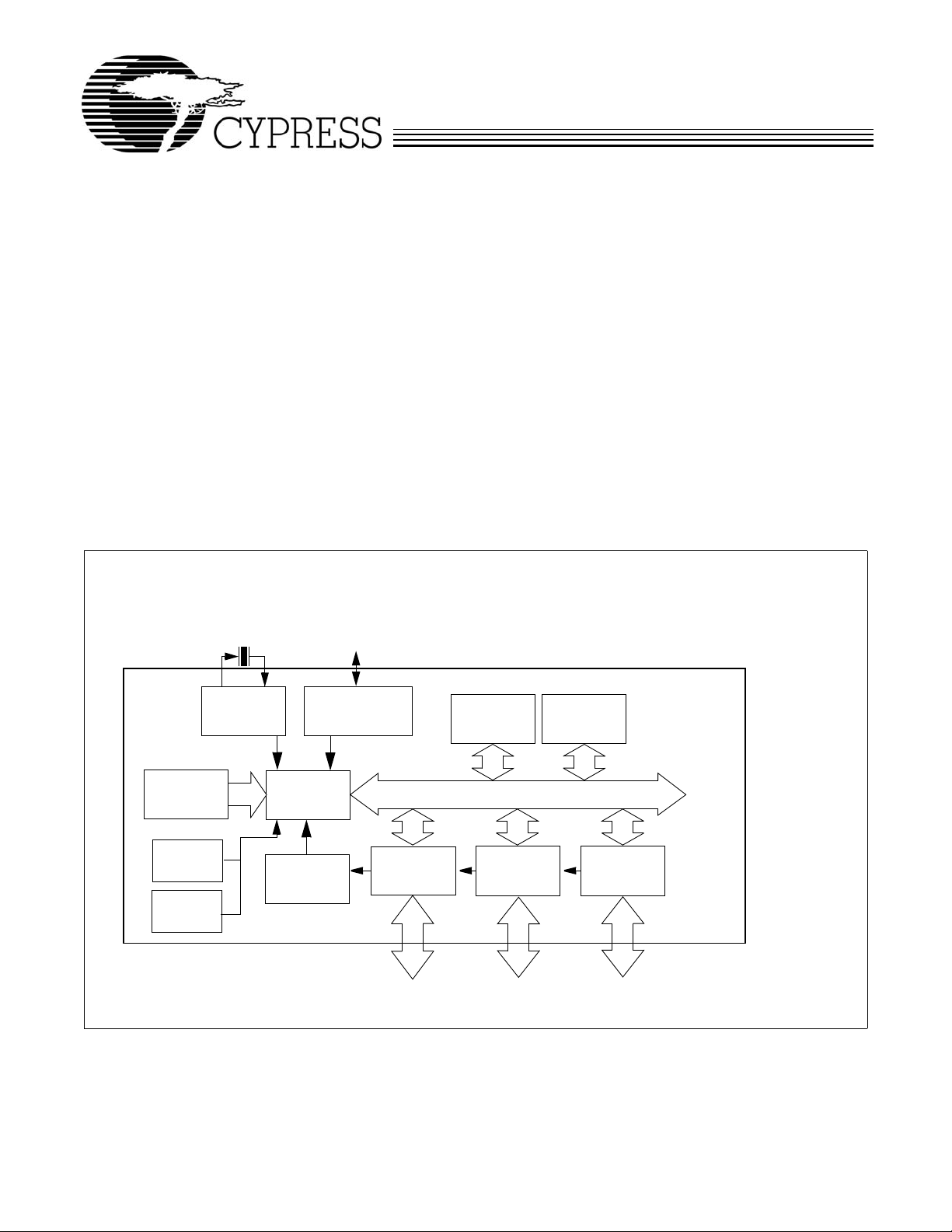
Logic Block Diagram
6-MHz
CERAMIC RESONATOR
R/C
EXT
—Integrated USB transceiver
—Up to 16 Schmitt trigger I/O pi ns with internal pull-up
—Up to eight I/O pins with LED drive capability
—Special p urpose I/O m ode supp orts optimization of
photo transistor and LED in mouse application
—Maskable Interrupts on all I/O pins
• 8-bit free-running timer
• Watchdog timer (WDT)
• Internal power-on reset (POR)
• Instant-On Now™ for Suspend and Periodic Wake-up
Modes
• Improved output drivers to reduce EMI
• Operating voltage from 4.0V to 5.25 VDC
• Operating temperature from 0–70°C
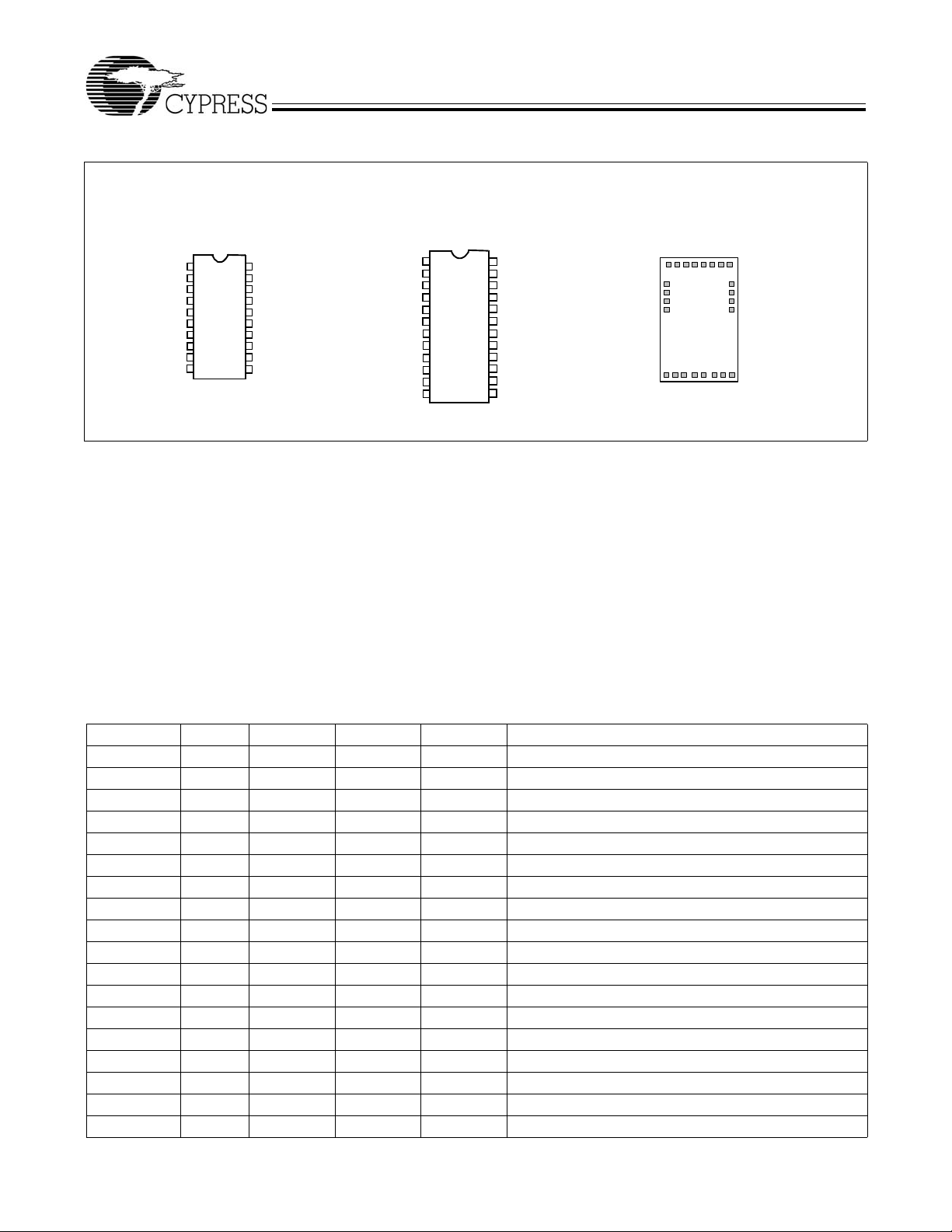
• Available in space saving and low-cost 20-pin PDIP,
20-pin SOIC, and 24-pin QSOP packages
• Industry-standard programmer support
EPROM
2/4 KByte
Power-
on Reset
Watch
Dog
Timer
OSC
INSTANT-ON
8-bit
RISC
core
Interrupt
Controller
NOW™
USB
Engine
D+,D–
VCC/V
SS
RAM
128-Byte
PORT
P0.0–P0.7
8-bit
Timer
PORT
0
1
P1.0–P1.7
Cypress Semiconductor Corporation • 3901 North First Street • San Jose, CA 95134 • 408-943-2600
Document #: 38-08026 Rev. *A Revised October 5, 2004
A
A
2.0 Pin Configurations
(Top View)
CY7C63001
CY7C63101
24-pin
SOIC/QSOP
P0.0
1
P0.1
2
P0.2
3
P0.3
4
P1.0
5
P1.2
6
P1.4
7
P1.6
8
V
9
SS
V
10
PP
11
12
P0.0
P0.1
P0.2
P0.3
P1.0
P1.2
V
V
CEXT
XTALIN
20-pin
DIP/SOIC
1
2
3
4
5
6
7
SS
8
PP
9
10
20
19
18
17
16
15
14
13
12
11
P0.4
P0.5
P0.6
P0.7
P1.1
P1.3
D+
D–
V
CC
XTALOUT
CEXT
XTALIN
3.0 Functional Overview
The CY7C630/101A is a family of 8-bit RISC One Time
Programmable (OTP) microc ontrollers with a built-in 1.5-Mbp s
USB Serial Interface Engine (SIE). The microcontroller
features 35 instructions that are optimized for USB applications. In addition, the microcontroller features 128 bytes of
internal RAM and four Kby tes of program memory sp ace. Th e
Cypress USB Controller accepts a 6-MHz ceramic resonator
as its cloc k source . This clock signal i s double d withi n the chi p
to provide a 12- MHz clock for the microprocessor.
The microcontroller features two ports of up to sixteen general
purpose I/Os (GPIOs). Each GPIO pin can be used to
generate an interrupt to the microcontroller. Additionally, all
CY7C63101A
DIE
P0.4
24
23
22
21
20
19
18
17
16
15
14
13
P0.5
P0.6
P0.7
P1.1
P1.3
P1.5
P1.7
D+
D–
V
CC
XTALOUT
4 3 2 1 24 23 22 21
5
6
7
8
13 14 15 16
9101112
20
19
18
17
pins in Port 1 are equipped with programmable drivers strong
enough to drive LEDs. The GPIO ports feature low EMI
emissions as a result of controlled rise and fall times and
unique output driver circuits. The Cypress microcontrollers
have a range of GPIOs to fit various applications; the
CY7C6300XA has twelve GPIOs and the CY7C6310XA has
sixteen GPIOs. Notice that each part has eight ‘low-current’
ports (Port 0) with the remaining ports (Port 1) being ‘highcurrent’ ports.
The 12-GPIO CY7C6300XA is available in 20-pin PDIP (-PC)
and 20-pin SOIC (-SC) packages. The 26-GPIO
CY7C6310XA is available in 24-pin QSOP (-QC) package.
4.0 Pin Definitions
Name I/O 20-Pin 24-pin Die Pad # Description
P0.0 I/O 1 1 1 Port 0 bit 0
P0.1 I/O 2 2 2 Port 0 bit 1
P0.2 I/O 3 3 3 Port 0 bit 2
P0.3 I/O 4 4 4 Port 0 bit 3
P0.4 I/O 20 24 24 Port 0 bit 4
P0.5 I/O 19 23 23 Port 0 bit 5
P0.6 I/O 18 22 22 Port 0 bit 6
P0.7 I/O 17 21 21 Port 0 bit 7
P1.0 I/O 5 5 5 Port 1 bit 0
P1.1 I/O 16 20 20 Port 1 bit 1
P1.2 I/O 6 6 6 Port 1 bit 2
P1.3 I/O 15 19 19 Port 1 bit 3
P1.4 I/O – 7 7 Port 1 bit 4
P1.5 I/O – 18 18 Port 1 bit 5
P1.6 I/O – 8 8 Port 1 bit 6
P1.7 I/O – 17 17 Port 1 bit 7
XT ALI N I 10 12 12 Ceramic resonator in
XT ALO UT O 11 13 13 Ceramic resona tor out
Document #: 38-08026 Rev. *A Page 2 of 25
CY7C63001
A
A
4.0 Pin Definitions (continued)
Name I/O 20-Pin 24-pin Die Pad # Description
CEXT I/O 9 11 11 Connects to external R/C timing circuit for optional
‘suspend’ wakeup
D+ I/O 14 16 16 USB data+
D– I/O 13 15 15 USB data–
V
PP
V
CC
V
SS
5.0 Pin Description
Name Description
V
CC
V
SS
V
PP
XTALIN One pin. Input from an external ceramic resonator.
XTALOUT One pin. Return path for the ceramic resonator (leave unconnected if driving XTALIN from an external
P0.0–P0.7,
P1.0–P1.7
D+, D– Two pins. Bidirectional USB data lines. An external pull-up resistor must be connected between the D pin
CEXT One pin. Open-drain output with Schmitt trigger input. The input is connected to a rising edge-triggered
– 8 1 0 10 Programming volt age supp ly , tie to groun d during no rmal
– 12 14 14 Voltage supply
– 7 9 9 Ground
One pin. Connects to the USB power source or to a nominal 5V power supply. Actual VCC range can vary
between 4.0V and 5.25V.
One pin. Connects to ground.
One pin. Used in prog ramming the o n-chip EPROM . This pin should be tied to groun d during norm al opera-
tions.
oscillator).
Sixteen pins. P0.0– P0.7 are t he 8 I/O l ines in Po rt 0. P1 .0–P1.7 are t he 8 I/O l ines in Port 1. P1 .0–P1.3 are
supported in the CY7C6300XA. All I/O pins include bit-programmable pull-up resistors. However, the sink
current of each pin can be programmed to one of sixteen levels. Besides functioning as GPIO lines, each
pin can be programmed as an interrupt input. The interrupt is edge-triggered, with programmable polarity.
and V
interrupt. CEXT may be connected to an external RC to generate a wake-up from Suspend mode. See
Section 6. 4.
to select low-speed USB operation.
CC
operation
CY7C63101
6.0 Functional Description
The Cypress CY7C630/101A USB microcontrollers are
optimized for human-interface computer peripherals such as
a mouse, joystic k, and ga mepad . These USB microcon trollers
conform to the low-spe ed (1.5 Mbps) req uirement s of the USB
Specification version 1.1. Each microcontroller is a selfcontained unit w ith: a USB interface engine, USB transceivers,
an 8-bit RISC microcontroller, a clock oscillator, timers, and
program memory. Each microcontroller supports one USB
device address and two endpoints.
The 6-MHz clock is doubled to 12 MHz to drive the microcontroller. A RISC architecture with 35 instructions provides the
best balance between performance and product cost.
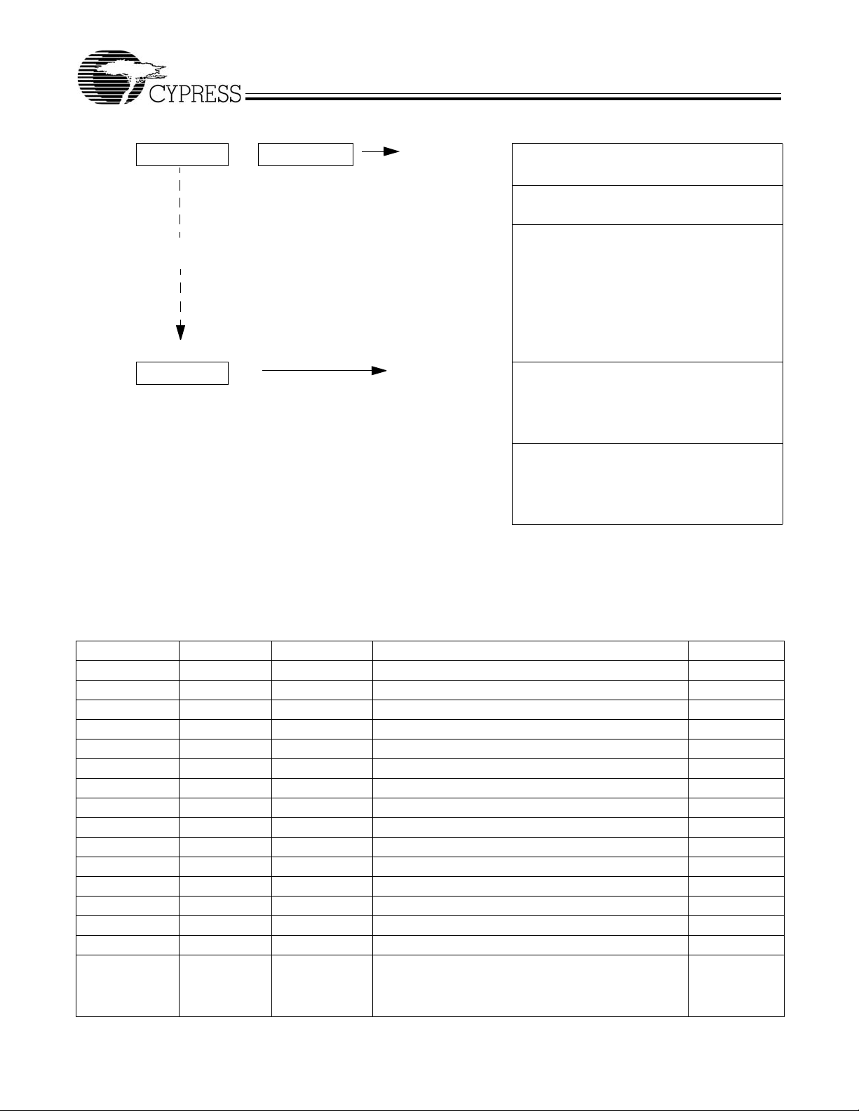
6.1.1 Program Memory Organization
The CY7C63001A and CY7C63101A each offer 4 Kbytes of
EPROM. The program memory space is divided into two
functional groups: interrupt vectors and program code.
The interrupt vectors occupy the first 16 bytes of the program
space. Each vec to r is 2 by tes l ong . Af t er a res et, th e Pro gram
Counter points to location zero of the program space. Figure
6-1 shows the organization of the Program Memory Space.
6.1.2 Security Fuse Bit
The Cypress USB microc ont roll er i ncl udes a security fus e bi t.
When the security fuse is programmed, the EPROM program
memory outputs 0xFF to the EPROM programmer, thus
protecting the user’s code.
6.1 Memory Organization
The memory in the USB Controller is organized into user
program memory in EPROM space and data memory in SRAM
space.
Document #: 38-08026 Rev. *A Page 3 of 25

A
A
after reset Address
PC 0x0000 Reset Vector
0x0002 Interrupt Vector – 128 µs
0x0004 Interrupt Vector – 1.024 ms
0x0006 Interrupt Vector – USB Endpoint 0
0x0008 Interrupt Vector – USB Endpoint 1
0x000A Reserved
0x000C Interrupt Vector – GPIO
0x000E Interrupt Vector – Cext
0x0010 On-chip program Memory
CY7C63001
CY7C63101
0x07FF 2K ROM (CY7C63000A, CY7C63100A)
0x0FFF 4K ROM (CY7C63001A, CY7C63101A)
Figure 6-1. Program Memory Space
6.1.3 Data Memory Organization
The USB Controller includes 128 bytes of data RAM. The
upper 16 bytes of the data memory are used as USB FIFOs
for Endpoint 0 and Endpoint 1. Ea ch endpoint is as sociated
with an 8-byte FIFO.
The USB controller includes two pointers into data RAM, the
Program Stack Pointer (PSP) and the Data Stack Pointer
(DSP). The value of PSP after reset is 0x00. The PSP increments by two whenever a CALL instruction is executed and it
decrements by two whenever a RET instru ction is used .
The DSP pre-decrements by one whenever a PUSH
instruction is executed and it increments by one after a POP
instruction is used. The defau lt v alu e of the DSP af ter res et i s
0x00, which would cause the first PUSH to write into USB
FIFO space for Endpoint 1. Therefore, the DSP should be
mapped to a location such as 0x70 before initiating any data
stack operations. Refer to the Reset section for more information about DSP remapping af ter reset. Figure 6-2 i llustrates
the Data Memory Space.
Document #: 38-08026 Rev. *A Page 4 of 25
CY7C63001
A
A
CY7C63101
after reset
DSP PSP
user
firmware
DSP
0x77
0x7F
Figure 6-2. Data Memory Space
Address
0x00
0x02
0x04
0x70 USB FIFO – Endpoint 0
0x78 USB FIFO – Endpoint 1
6.2 I/O Register Summary
I/O registers are accessed via the I/O Read (IORD) and I/O
Write (IOWR, IOWX) instruc tions.
Table 6-1. I/O Register Summary
Register Name I/O Address Read/Write Function Page
P0 Data 0x00 R/W General purpose I/O Port (low current) Figure 6-8
P1 Data 0x01 R/W General purpose I/O Port (high current) Figure 6-9
P0 IE 0x04 W Interrupt enable for Port 0 pins Figure 6-17
P1 IE 0x05 W Interrupt enable for Port 1 pins Figure 6-18
P0 Pull-up 0x08 W Pull-up resistor control for Port 0 pins Figure 6-11
P1 Pull-up 0x09 W Pull-up resistor control for Port 1 pins Figure 6-12
EP0 TX Config. 0x10 R/W USB Endpoint 0 transmit configuration Figure 6-22
EP1 TX Config. 0x11 R/W USB Endpoint 1 transmit configuration Figure 6-23
USB DA 0x12 R/W USB device address Figure 6-20
USB SCR 0x13 R/W USB status and control Figure 6-24
EP0 RX Status 0x14 R/W USB Endpoint 0 receive status Figure 6-21
GIE 0x20 R/W Global Interrupt Enable Figure 6-15
WDT 0x21 W Watchdog Timer clear Figure 6-4
Cext 0x22 R/W External R-C Timing circuit control Figure 6-5
Timer 0x23 R Fre e-ru nni ng timer Figure 6-6
P0 Isink 0x30-0x37 W Input sink current control for Port 0 pins. There is one
Isink register for each pin. Address of the Isink register
for pin 0 is located at 0x30 and the register address for
pin 7 is located at 0x37.
Figure 6-13
Document #: 38-08026 Rev. *A Page 5 of 25
CY7C63001
A
A
Table 6-1. I/O Register Summary (continued)
Register Name I/O Address Read/Write Function Page
P1 Isink 0x38-0x3F W Input sink current control for Port 1 pins. There is one
Isink register for each pin. Address of the Isink register
for pin 0 is located at 0x38 and the register address for
pin 7 is located at 0x3F. The number of Port 1 pins
depends on package type.
SCR 0xFF R/W Processor status and control register Figure 6-3
CY7C63101
Figure 6-13
6.3 Reset
The USB Controller supports three types of resets. All
registers are restored to theirW atchdog defaul t states during a
reset. The USB Device Address is set to 0 and all interrupts
are disabled. In addition, the Program Stack Pointer (PSP) is
set to 0x00 and the Data Stack Pointer (DSP) is set to 0x00.
The user should set the DSP to a location such as 0x70 to
reserve 16 bytes of USB F IFO spac e. The assem bly in struc tions to do so are:
MOV A, 70h ; Move 70 hex into Accumulator, use 70
instead of 6F because the dsp is
; always decremented by 1 befo re the
data transfer of the PUSH instruction occurs
SWAP A, DSP ; Move Accumulator value into dsp
The three reset types are:
1. Power-On Reset (POR)
2. Watchdog Reset (WDR)
3. USB Reset
b7 b6 b5 b4 b3 b2 b1 b0
Reserved WDR USBR POR SUSPEND Reserved Reserved RUN
R/W R/W R/W R/W R/W
00010001
Figure 6-3. Status and Control Register (SCR – Address 0xFF)
The occurrence of a reset is rec orded in the St atus and Control
Register located at I/O address 0xFF (Figure 6-3). Reading
and writing this re gister are supported by the IORD and IOWR
instructions. Bit s 1, 2 , an d 7 are re served and must be written
as zeros during a write. During a read, reserved bi t positions
should be ignored. Bits 4, 5, and 6 are used to record the
occurrence of POR, USB, and WDR Reset respectively. The
firmware can interrogate these bits to determine the cause of
a reset. If a Watchdog Rese t occurs, firmware must clear the
WDR bit (bit 6) in the S tatu s and Control Regi ster to re-enabl e
the USB transmitter (please refer to the Watchdog Reset
section for further details). Bit 0, the “Run” control, is set to 1
at POR. Clearing this bit stops the microcontroller (firmware
normally should n ot cl ear thi s bit). Once this bit is set to LOW,
only a reset can set this bit HIGH.
The microcontroller resumes execution from ROM address
0x00 after a reset unless the Suspend bit (bit 3) of the Status
and Control Register is set. Setting the Suspend bit stops the
clock oscillator and the interrupt timers and powers down the
microcontroller. The detection of any USB activity, the occurrence of a GPIO Interrupt, or the occurrence of the Cext
Interrupt terminates the suspend condition.
6.3.1 Power-On Reset
Power-On Reset (POR) occurs every time the power to the
device is switche d on. Bit 4 o f the Status and Control Register
is set to record this event (the register contents are set to
00011001 by the POR). The USB Controller is placed in
Document #: 38-08026 Rev. *A Page 6 of 25
suspended mode at the end of POR to conserve power (the
clock oscillator, the timers, and the interrupt logic are turned
off in suspend mode). After POR, only a non-idle USB Bus
state terminates the suspend mode. The microcontroller then
begins execution from ROM address 0x00.
CY7C63001
A
A
CY7C63101
7.168 to
8.192 ms
Last write to
Watchdog Timer
Register
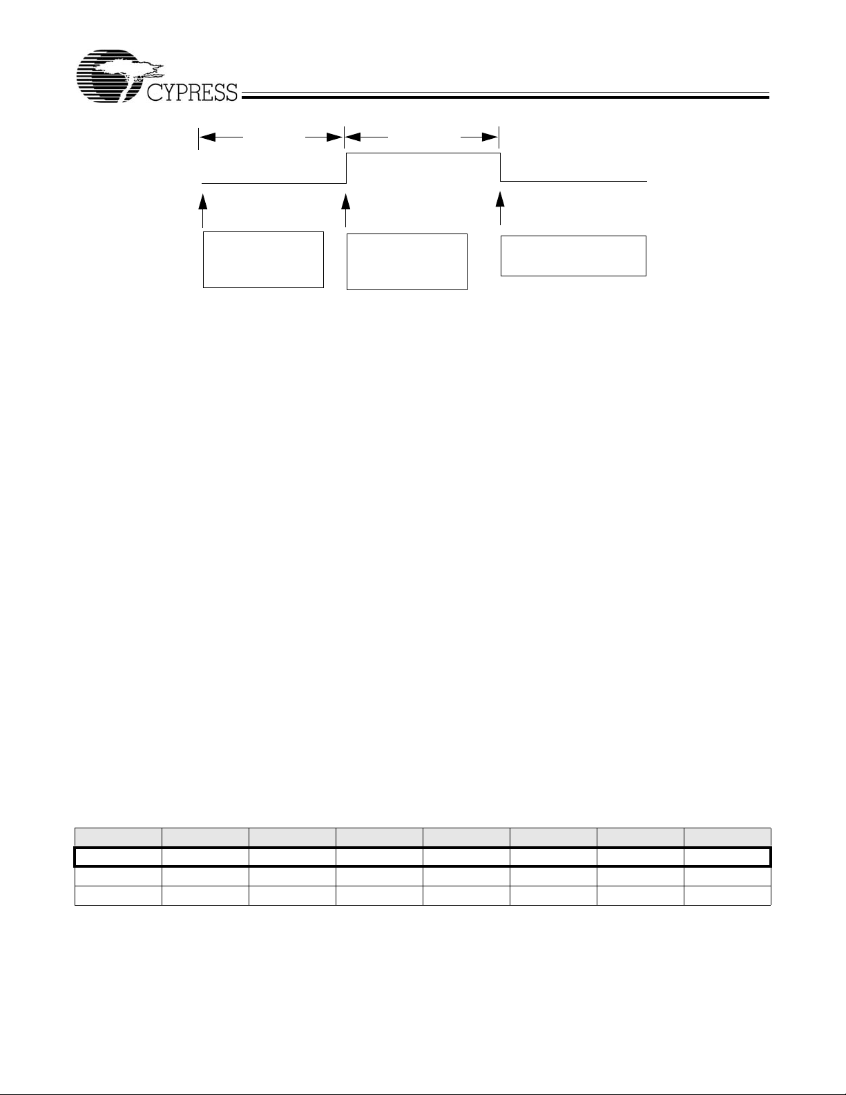
6.3.2 Watchdog Reset (WDR)
The Watchdog Timer Reset (WDR) occurs when the Most
Significant Bit of the 4- bit W atchdog T imer Register transition s
from LOW to HIGH. Writing any value to the write-only
Watchdog Restart Register at 0x21 clears the timer (firmware
should periodically write to the Watchdog Restart Register in
the ‘main loop’ of fir mware). The W atchdog ti mer is clocked b y
a 1.024-ms clock from the fre e-runni ng tim er. If 8 clocks occur
between writes to the timer, a WDR occurs and bit 6 of the
Status and Control Register is set to record the event. A
Watchdog Timer Reset lasts for 8.192 ms, at which time the
microcontroller begins execution at ROM address 0x00. The
USB transmitter is disab led by a Watch dog Reset becau se the
USB Device Address Regist er is cleared (otherwise, the USB
Controller would respond to all address 0 transactions). The
transmitter remains disabled until the WDR bit (bit 6) in the
Status and Control Register is reset to 0 by firmware.
6.3.3 USB Bus Reset
The USB Controller recognizes a USB Reset when a Single
Ended Zero (SE0) condition persists for at least 8–16 µs (the
Reset may be reco gn ized f or an SE0 as s hort as 8 µs, but it is
always recognized for an SE0 longer than 16 µs). SE0 is the
condition in which both the D+ line and the D– line are LOW.
Bit 5 of the Status and Control Register is set to record this
event. If the USB reset happens while the device is
suspended, the suspend condition is cleared and the clock
oscillator is restarted. However, the microcontroller is not
released until the USB reset is removed.
No write to WDT
register, so WDR
goes HIGH
Figure 6-4. Watchdog Reset
6.4 Instant-on Feature (Suspend Mode)
The USB Controller can be placed in a low-power state by
setting the Suspend bit (bit 3) of the Status and Control
8.192 ms
Execution begins at
Reset Vector 0x00
register . Al l log ic bl ocks in the de vice are t urned of f e xcept the
USB receiver, the GPIO interrupt logic, and the Cext interrupt
logic. The clock oscil lat or and the fre e-running and Watchdog
timers are shut down.
The suspend mode is terminated when one of the following
three conditions occur:
1. USB activity
2. A GPIO interrupt
3. Cext interrupt
The clock oscillator, GPIO, and timers restart immediately
upon exiting suspend mode. The USB engine and microcontroller return to a fully functional state no more than 256 µs
later. Before servicing any interrupt requests, the microcontroller executes the instruction following the I/O write that
placed the device into suspend mode.
Both the GPIO interrupt and the Cext interrupt allow the USB
Controller to wake-up periodically and poll potentiometers,
optics, and othe r system com ponents while maint aining a very
low average power consumption. The Cext Interrupt is
preferred for lowest power consum ption.
For Cext to generate an “I nst ant-on” i nterrupt , the pin must b e
connected to groun d with an external c apacitor and co nnected
with an external resistor. A “0” is written to the Cext
to V
CC
register located at I/O address 0x22 to discharge the capacitor .
Then, a “1” is w ritten to d isabl e the open -drain output driv er. A
Schmitt trigger input circuit monitors the input and generates
a wake-up interrupt when the input voltage rises above the
input threshold. By changing the va lues of the external resistor
and capacitor, the user can fine tune th e c ha r ge rate of the R C timing circuit. The format of the Cext register is shown in
Figure 6-5. Reading the register returns the value of the Cext
pin. During a reset, the Cext pin is HIGH.
b7 b6 b5 b4 b3 b2 b1 b0
Reserved Reserved Reserved Reserved Reserved Reserved Reserved CEXT
R/W
00000001
Figure 6-5. The Cext Register (Address 0x22)
Document #: 38-08026 Rev. *A Page 7 of 25
CY7C63001
A
A
CY7C63101
6.5 On-Chip Timer
The USB Controller is equipped with a free-running timer
driven by a c lock one-sixth the resonator frequency. Bits 0
through 7 of the cou nter are readable fr om the read-only T imer
Register located at I/O address 0x23. The Timer Register is
cleared during a Power-On Reset and whenever Suspend
Figure 6-6. Timer Register (Address 0x23)
b7 b6 b5 b4 b3 b2 b1 b0
T.7 T.6 T.5 T.4 T.3 T.2 T.1 T.0
RRRRRRRR
00000000
mode is entered. Figure 6-6 illustrates the format of this
register and Figure 6-7 is its block diagram.
With a 6 MHz resonator, the timer resolution is 1 µs.
The timer generates two interrupts: the 128-µs interrupt and
the 1.024-ms interrupt.
1.024-ms interrupt
128-
m
s interrupt
9
8
7
6
5
4
3
2
1
0
Resonator Clock/6
8
To Timer Register
Figure 6-7. Timer Block Diagram
6.6 General Purpose I/O Ports
Interface with peripherals is conducted via as many as 16
GPIO signals. Th es e s ig nal s are d iv ide d into two ports: Port 0
and Port 1. Port 0 contains eig ht li nes (P0.0 –P0. 7) and P ort 1
contains up to eig ht lines (P1.0– P1.7). The numb er of external
I/O pins depends on the package type. Both ports can be
accessed by the IORD, IOWR, and IOWX instructions. The
b7 b6 b5 b4 b3 b2 b1 b0
P0.7 P0.6 P0.5 P0.4 P0.3 P0.2 P0.1 P0.0
R/W R/W R/W R/W R/W R/W R/W R/W
1 1 1 1 1 1 1 1
Figure 6-8. Port 0 Data Register (Address 0x00)
b7 b6 b5 b4 b3 b2 b1 b0
P1.7 P1.6 P1.5 P1.4 P1.3 P1.2 P1.1 P1.0
R/W R/W R/W R/W R/W R/W R/W R/W
1 1 1 1 1 1 1 1
Figure 6-9. Port 1 Data Register (Address 0x01)
Port 0 data register is located at I/O address 0x00 while the
Port 1 data register is located at I/O address 0x01. The
contents of both registers are set HIGH during a reset. Refer
to Figures 6-8 and 6-9 for the formats of the data registers. In
addition to supporting general inp ut/output fu nctions, each I/O
line can trigger an in terrupt to th e microcon troller. Please refer
to the interrupt section for more details.
Document #: 38-08026 Rev. *A Page 8 of 25

CY7C63001
A
A
V
CY7C63101
Each GPIO line inc lu des a n i nte rnal R
provides both the pull-up function and slew control. Two
factors govern th e enab ling a nd di sabli ng of e ach re sisto r: the
state of it s a ss oc iat ed Port Pull-up register bit and the state of
the Data Register bit. NOTE: The control bits in the Port Pullup register are active LOW.
A GPIO line is HIGH when a “1” is written to the Data Register
and a “0” is written to the respective Port Pull-up register.
Writing a “0” to the port Data Register disables the port ’ s Pul lup resistor and output s a L OW on the GPI O line regardle ss of
the setting in the Port Pull-up Register. The output goes to a
high-Z state if the Data Register bit and the Port Pull-up
Register bit are both “1”. Figure 6-10 illustrates the block
Port Pull-Up
Register
Port Data
Register
Port Isink
Register
Suspend
Bit
resistor. This resistor
up
Isink
DAC
Disable
diagram of one I/O line. The Port Isink Register is used to
control the output current level and it is described later in this
section. NOTE: The Isink logic block is turned off during
suspend mode (please refe r to th e Ins t an t-on Fea t ure sec tio n
for more details). Therefore, to prevent higher I
during USB suspend mode, firmware must s et ALL Port 0 and
Port 1 Data Register bits (which are not externally driven to a
known state), includ ing those that are not bon ded out on a
particular package, to “1” and all Port 0 and Port 1 Pull-Up
Register data bits to “0” to enable port pull-ups before setting
the Suspend bit (bit 3 of the Status and Control Register).
Table 6-2 is the Output Control truth table.
CC
R
up
GPIO
Pin
Schmitt
Trigger
currents
CC
Data Bus
Figure 6-10. Block Diagram of an I/O Line
Table 6-2. Output Control Truth Table
Data Register Port Pull-up Register Output at I/O Pin Interrupt Polarity
0 0 Sink Current (‘0’) High to Low
0 1 Sink Current (‘0’) Low to High
1 0 Pull-up Resistor (‘1’) High to Low
1 1 Hi-Z Low to High
To configure a GPIO pin as an in put, a “1” sho uld be writt en to
the Port Data Register bit associated with that pin to disable
the pull-down function of the Isink DAC (see Figure 6-
10).When the Port Data Register is read, the bit value is a “1”
if the voltage on the pin is greater than the Schmitt trigger
threshold, or “0” if it is below the threshold. In applications
where an internal pull-up is required, the R
can be engaged by writin g a “0” to the appropriate bit in the
Port Pull-up Register.
b7 b6 b5 b4 b3 b2 b1 b0
PULL0.7 PULL0.6 PULL0.5 PULL0.4 PULL0.3 PULL0.2 PULL0.1 PULL0.0
WWWWWWWW
00000000
Figure 6-11. Port 0 Pull-up Register (Address 0x08)
pull-up resistor
up
Both Port 0 and Port 1 Pull-up Register s are wri te only (s ee
Figures 6-11 and 6-12). The Port 0 Pull-u p Re gis te r is loc ate d
at I/O address 0x08 and Port 1 Pull-up Register is mapped to
address 0x09. The contents of the Port Pull-up Registers are
cleared during reset, allowing the outputs to be controlled by
the state of the Data Registers. The Port Pull-up Re gisters also
select the polarity of transition that gen erates a GPIO interrup t.
A “0” selects a HIGH to LOW transition while a “1” selects a
LOW to HIGH transition.
Document #: 38-08026 Rev. *A Page 9 of 25

CY7C63001
A
A
b7 b6 b5 b4 b3 b2 b1 b0
PULL1.7 PULL1.6 PULL1.5 PULL1.4 PULL1.3 PULL1.2 PULL1.1 PULL1.0
WWWWWWWW
0x0000000
Figure 6-12. Port 1 Pull-up Register (Address 0x09)
CY7C63101
Writing a “0” to the Data Register drives the output LOW.
Instead of providing a fixed output drive, the USB Controller
allows the user to select an output sink current level for each
I/O pin. The sink current of each output is controlled by a
b7 b6 b5 b4 b3 b2 b1 b0
Reserved Reserved Reserved UNUSED ISINK3 ISINK2 ISINK1 ISINK0
WWWWWWWW
xxxxxxxx
Figure 6-13. Port Isink Register for One GPIO Line
Port 0 is a low-current port suitable for connecting photo
transistors. Port 1 is a high current port capable of driving
LEDs. See section 8.0 for current ranges. 0000 is the lowest
drive strength. 1111 is the highest.
The write-only sink current control registers for Port 0 outputs
are assigned from I/O address 0x30 to 0x37 with the control
bits for P00 starting at 0x30. Port 1 sink current control
registers are assigne d from I/O addres s 0x38 to 0x3F with the
control bits f or P10 starting at 0x 38. All sink curre nt control
clk1x
(to USB SIE)
clk2x
(to Microcontroller)
Clock
Doubler
dedicated Port Isink Register. The lower four bits of this
register contain a code selecting one of sixteen sink current
levels. The upper four bits of the register are ignored. The
format of the Port Isink Register is shown in Figure 6-13.
registers are cleared during a reset, resulting in the minimum
current sink setting.
6.7 XTALIN/XTALOUT
The XTALIN and XTALOUT pins support connection of a 6MHz ceramic resonator. The feedback capacitors and bias
resistor are internal to the IC, as shown in Figure 6-14 Leave
XT ALOUT unconnecte d when driving XT AL IN from an ext ernal
oscillator.
XTALOUT
XTALIN
30 pF30 pF
Figure 6-14. Clock Oscillator On-chip Circuit
6.8 Interrupts
Interrupts are genera ted by the General Purpose I/O lines, the
Cext pin, the internal time r, and the USB engine. All interrupts
are maskable by the Globa l Interrupt Enabl e Registe r . Acces s
to this register is accomplished via IORD, IOWR, and IOWX
b7 b6 b5 b4 b3 b2 b1 b0
CEXTIE GPIOIE Reserved EP1IE EP0IE 1024IE 128IE Reserved
R/W R/W R/W R/W R/W R/W
00000000
Figure 6-15. Global Interrupt Enable Register (GIER – Address 0x20)
The interrupt controller contains a separate latch for each
interrupt. See Figure 6-16 for the logic block diagram for the
interrupt controller. When an interrupt is generated, it is
latched as a pending interrupt. It stays as a pending interrupt
until it is se rviced or a reset oc curs. A pe nding i nterrup t only
Document #: 38-08026 Rev. *A Page 10 of 25
instructions to address 0x20. Writing a “1” to a bit position
enables the interrupt associated with that position. During a
reset, the contents of the Interrupt Enable Register are
cleared, disabling all interrupts. Figure 6-15 illustrates the
format of the Global Interrupt Enable Register.
generates an interrupt request if it is enabled in the Global
Interrupt Enable Register. The highest priority interrupt
request is serviced following the execution of the current
instruction.

CY7C63001
A
A
CY7C63101
When servicing an interrupt, the hardware first disables all
interrupts by clearing the Global Interrupt Enable Register.
Next, the interrupt latch of the current interrupt is cleared. Thi s
is followed by a CALL instruction to the ROM address
associated with the interrupt being serviced (i.e., the interrupt
vector). The instruc ti on in the interrupt table is typical ly a JM P
instruction to the address of the Interrupt Service Routine
(ISR). The user can re -enable interrupt s in the interrupt s ervice
routine by writing to the a ppropriate b its in th e Global Interru pt
Enable Register. Interrupts can be nested to a level limited
only by the available stack space.
The Program Counter (PC) val ue and the Carry and Z ero flags
(CF, ZF) are automatically stored onto the Program Stack by
the CALL instruction as part of the interrupt acknowledge
Table 6-3. Interrupt Vector Assignments
Interrupt Priority ROM Address Function
0 (Highest) 0x00 Reset
1 0x02 128-µs timer interrupt
2 0x04 1.024-ms timer interrupt
3 0x06 USB endpoint 0 interrupt
4 0x08 USB endpoint 1 interrupt
5 0x0A Reserved
6 0x0C GPIO interrupt
7 (Lowest) 0x0E Wake-up interrupt
process. The user firmware is res ponsible for ens uring that the
processor state is pres erv ed a nd re sto r ed durin g an int errup t.
For example the PUSH A instruction should be used as the
first command in the ISR to save the accumulator value. And,
the IPRET instruction should be used to exit the ISR with the
accumulator value restored and interrupts enabled. The PC,
CF, and ZF ar e res t or e d wh en th e IP RE T o r RE T i ns tr uc t io ns
are executed.
The Interrupt Vectors supported by the USB Controller are
listed in Table 6-3. Interrupt Vector 0 (Reset) has the highest
priority, Interrupt Vector 7 has the lowe st p r io rity. Because the
JMP instruction is two bytes long, the interrupt v ectors occup y
two bytes.
6.8.1 Interrupt Latency
Interrupt latency can be calculated from the following
equation:
Interrupt Latency = (Number of clock cyc les remaining i n the
current instruction) + (10 clock cycles for
the CALL instru ction) + (5 clock cycles
for the JMP inst ruction)
m
s
CLR
DQ
CLK
CLR
DQ
CLK
CLR
DQ
CLK
Enable [1]
Enable [6]
Enable [7]
Global
Interrupt
Enable
Register
CLR
Interrupt
Acknowledge
Logic 1
128-
Interrupt
Enable [7:0]
Logic 1
GPIO
Interrupt
Logic 1
CEXT
For example, if a 5-c lock- cycle i nstruc tion s uch as JC i s bein g
executed when an interrupt occurs, the first instruction of the
Interrupt Service Routine executes a minimum of 16 clock
cycles (1+10+5) or a maximum of 20 clock cycles (5+10+5)
after the interrupt is issued. The refo r e, the int errup t late ncy in
this example will be = 20 cloc k periods = 20 / (12 MHz) = 1.667
µs. The interrupt latches are samp led at the ri sing ed ge of the
last clock cycle in the current instruction.
128-
m
s CLR
128-ms IRQ
1-ms CLR
1-ms IRQ
End P0 CLR
End P0 IRQ
End P1 CLR
End P1 IRQ
GPIO CLR
GPIO IRQ
Wake-up CLR
Wake-up IRQ
Interrupt
Priority
Encoder
IRQ
Interrupt
Vector
Figure 6-16. Interrupt Controller Logic Block Diagram
Document #: 38-08026 Rev. *A P age 11 of 25

CY7C63001
A
A
CY7C63101
6.8.2 GPIO Interrupt
The General Purpose I/O interrupts are generated by signal
transitions at the Port 0 and Port 1 I/O pins. GPIO interrupts
are edge sensitive with programmable interrupt polarities.
Setting a bi t H IGH i n t he Po r t P u l l-u p Re gi ste r (s ee Figure 6-
11 and 6-12) selects a LOW to HIGH interrupt trigger for the
corresponding por t pin. Set ting a b it LOW activ ates a HIGH to
LOW interrupt trigger. Each GPIO interrupt is maskable on a
per-pin basis by a dedicated bit in the Port Interrupt Enable
Register. Writing a “1” enables the interrupt. Figure 6-17 and
Figure 6-18 illustrate the format of the Port Interrupt Enable
Registers for Port 0 and Port 1 lo cated at I/O address 0x04 an d
0x05 respectively. These write only registers are cleared
during reset, thus disabling all GPIO interrupts.
b7 b6 b5 b4 b3 b2 b1 b0
IE0.7 IE0.6 IE0.5 IE0.4 IE0.3 IE0.2 IE0.1 IE0.0
WWWWWWWW
00000000
Figure 6-17. Port 0 In terrupt Enable Register (P0 IE – Address 0x04)
b7 b6 b5 b4 b3 b2 b1 b0
IE1.7 IE1.6 IE1.5 IE1.4 IE1.3 IE1.2 IE1.1 IE1.0
WWWWWWWW
00000000
Figure 6-18. Port 1 In terrupt Enable Register (P1 IE – Address 0x05)
A block diagram of the GPIO interrupt logi c is shown in Figure
6-19. The bit setting in the Port Pull-up Register selects the
interrupt polarity. If the selected signal polarity is detected on
the I/O pin, a HIGH signal is generated. If the Port Interrupt
Enable bit for this pin is HIGH and no other port pins are
requesting interrupts, the OR gate issues a LOW to HIGH
signal to clock the GPIO interrupt flip-flop. The output of the
flip-flop is further qual ified by the Global GPIO In terrupt Enable
bit before it is processe d by the Interrupt Priority Encoder . Both
the GPIO interrupt flip-flop an d the Global GPIO Enable bi t are
cleared by on-chip hardware during GPIO interrupt
acknowledge.
GPIO
Pin
1 = Enable
0 = Disable
Interrupt
Acknowledge
Port
Pull-Up
Register
M
U
X
Port Inte rrupt
Enable Register
1 = Enable
0 = Disable
1=L→H
Æ
L
0=H
CLR
Global
GPIO In t e r r upt
Enable
(Bit 6, Register 0x20)
Figure 6-19. GPIO Interrupt Logic Block Diagram
Note. If one port pin tri ggers an interrupt, no other port pin can
cause a GPIO interrupt until the port pin that triggered the
interrupt has returned to its inactive (non-trigger) state or until
its corresponding port interrupt enable bit is cleared (these
events ‘reset’ the clock of the GPIO Interrupt flip-flop, which
must be ‘reset’ to ‘0’ before another GPIO interrupt event can
‘clock’ the GPIO Interrupt flip-flop and produce an IRQ).
Note. If the port pin that triggered an interrupt is held in its
active (trigger) state while its corresponding port interrupt
GPIO In te rr u pt
I
Flip-Flop
D
Q
CLR
Interrupt
Priority
Encoder
IRQ
Interrupt
Vector
OR Gate
(1 input per
GPIO pin)
enable bit is cleared and then set, a GPIO interrupt event
occurs as the GPIO Interrupt flip-flop clock transition s f rom ‘1 ’
to ‘0’ and then back to ‘1’ (please refer to Figure 6-19). The
USB Controller does not assign interrupt priority to different
port pins and the Port Interrupt Enable Registers are not
cleared during the interrupt acknowledge process. When a
GPIO interrupt is serviced, the ISR must poll the ports to
determine which pin caused the interrupt.
Document #: 38-08026 Rev. *A Page 12 of 25

CY7C63001
A
A
CY7C63101
6.8.3 USB Interrupt
A USB Endpoint 0 interrupt is generated after the host has
written data to Endpoint 0 or after the USB Controller has
transmitte d a packet from Endpoint 0 a nd receives an ACK
from the host. An OUT packet from the host which is NAKed
by the USB Controller does not generate an interrupt. This
interrupt is maske d by the USB E P0 Interru pt Enable bit (bit 3)
of the Global Interrupt Enable Register.
A USB Endpoint 1 interrupt is generated after the USB
Controller has transmitted a packet from Endpoint 1 and has
received an ACK from the host. This interrupt is m asked by the
USB EP1 Interrupt Enable bit (bit 4) of the Global Interrupt
Enable Register.
6.8.4 Timer Interrupt
There are two timer interrupts: the 128-µs interrupt and the
1.024-ms interrupt. They are masked by bits 1 and 2 of the
Global Interrupt Ena ble Register respe ctively . The u ser should
disable both timer interrupts before going into the suspend
mode to avoid pos sible conflicts from timer interru pts occurring
just as suspend mode is entered.
6.8.5 Wake-Up Interrupt
A wake-up interrupt is generated when the Cext pin goes
HIGH. This interrupt is latche d in the inte rrupt control ler . It ca n
be masked by th e Wake-up Inte rrupt Enable bit (bit 7) of the
Global Interrupt Enable Regi ster . This interru pt can be used to
perform periodic checks on attached peripherals when the
USB Controller is placed in the low-power suspend mode. See
the Instant-On Feature section for more details.
6.9 USB Engine
The USB engine includes the Serial Interface Engine (SIE)
and the low-speed USB I/O transceivers. The SIE block
performs most o f the USB interface fu nctions with only minimal
support from the microcontroller core. Two endpoints are
supported. Endpoint 0 is used to receive and transmit control
(including setup) packets while Endpoint 1 is only used to
transmit data packets.
The USB SIE processes USB bus activity at the transaction
level independently. It does all the NRZI encoding/decoding
and bit stuffing/unstuffing. It also determines token type,
checks addres s and endpoint va lues, genera tes and checks
CRC values, and controls the flow of data bytes between the
bus and the Endpoint FIFO s. NOTE: the SIE stal ls the CPU for
three cycles per byte when writing da t a to the endpo int FIFO s
(or 3 * 1/12 MHz * 8 bytes = 2 µs per 8-byte transfer).
The firmware handles hi gher level an d function-sp ecific t asks.
During control transfers the firmware must interpret device
requests and respond correctly. It also must coordinate
Suspend/Resume, verify and select DATA toggle values, and
perform function specific tasks.
The USB engine and the firmware communicate though the
Endpoint FIFOs, USB Endpoint interrupts, and the USB
registers described in the sections below.
6.9.1 USB Enumeration Process
The USB Controller pro vi des a USB Device Address Register
at I/O location 0x12. Reading and writing this register is
achieved via the IORD and IOWR instructions. The register
contents are cleared during a reset, setting the USB address
of the USB Controller to 0. Figure 6-20 shows the format of the
USB Address Register.
b7 b6 b5 b4 b3 b2 b1 b0
Reserved ADR6 ADR5 ADR4 ADR3 ADR2 ADR1 ADR0
R/W R/W R/W R/W R/W R/W R/W
00000000
Figure 6-20. USB Device Address Register (USB DA – Address 0x12)
Typical enumeration steps:
1. The host computer sends a SETUP packet fo llowed by a
DATA packet to USB address 0 requesting the Device
descriptor.
2. The USB Controller decodes the request and retrieves its
Device descriptor from the program memory space.
3. The host computer performs a contro l rea d s equ enc e a nd
the USB Controller responds by sending the Device
descriptor over the USB bus.
4. After receiving the descriptor, the host computer sends a
SETUP packet followed by a DATA packet to address 0
assigning a new USB address to the device.
5. The USB Controller stores the new address in its USB
Device Address Register after the no-data control
sequence complete s.
6. The host sends a request for the Device descriptor using
the new USB address.
7. The USB Controller decodes the request and ret rieves the
Device descriptor from the program memory.
8. The host performs a control read sequence and the USB
Controller responds by sending its Device descriptor over
the USB bus.
9. The host generates control reads to the USB Contro lle r to
request the Configuration and R epo rt desc rip tors .
10.The USB Controller retrieves the descriptors from its
program space and returns the data to the host over the
USB.
1 1.Enumeration is complete after the host has received al l the
descriptors.
Document #: 38-08026 Rev. *A Page 13 of 25

CY7C63001
A
A
CY7C63101
6.9.2 Endpoint 0
All USB devices are required to have an endpoint number 0
that is used to in iti alize and man ip ulate the de vice. End point 0
provides access to the device’s configuration information and
allows generic USB status and control accesses.
Endpoint 0 ca n receive and t ransmit data. B oth receive a nd
transmit data share the same 8-byte Endpoint 0 FIFO located
at data memory space 0x70 to 0x77. Received data may
overwrite the data previously in the FIFO.
b7 b6 b5 b4 b3 b2 b1 b0
COUNT3 COUNT2 COUNT1 COUNT0 TOGGLE IN OUT SETUP
R/W R/W R/W R/W R R/W R/W R/W
00000000
Figure 6-21. USB Endpoint 0 RX Register (Address 0x14)
This is a read/write register located at I/O address 0x14. Any
write to this register clears all bits except bit 3 which remains
unchanged. All bits are cleared during reset.
Bit 0 is set to 1 when a SETUP token for Endpoi nt 0 is received.
Once set to a 1, this bit remains HIGH until it is cleared by an
I/O write or a reset . While the dat a following a SETUP is b eing
received by the USB e ngine, this bit is not clea red by an I/O
write. User firmware writes to the USB FIFOs are disabled
when bit 0 is set. This prevents SETUP data from being
overwritten.
Bits 1 and 2 are updated whenever a valid token is received
on Endpoint 0. Bit 1 is set to 1 if an OUT toke n is receiv ed and
cleared to 0 if any othe r toke n is received . Bit 2 is s et to 1 if a n
IN token is received and cleared to 0 if any other token is
received.
Bit 3 shows the Data Toggle status of DATA packets received
on Endpoint 0. This bit is updated for DATA following SETUP
tokens and for DATA following OUT tokens if Stall (bit 5 of
0x10) is not set and either EnableOuts or StatusOuts (bits 3
and 4 of 0x13) are set.
Bits 4 to 7 are the count of the number of bytes received in a
DATA packet. The two CRC bytes are included in the count,
so the count value is two g reater than the number of da ta bytes
6.9.2.1 Endpoint 0 Receive
After receiving a packet and placing the data into the Endpoint
0 FIFO, the USB Controller updates the USB Endpoint 0 RX
register to record the receive sta tus and then generates a USB
Endpoint 0 interrupt. The format of the Endpoint 0 RX Register
is shown in Figure 6-21.
received. The cou nt i s always updated and the data is alway s
stored in the FIFO for DATA packets following a SETUP token.
The count for DATA fol lowi ng an OUT token is updated if Stall
(bit 5 of 0x10) is 0 and either EnableOuts or StatusOuts (bits
3 and 4 of 0x13) are 1. The DATA following an OUT is written
into the FIFO if EnableOuts is set to 1 and S tal l and S tatusOut s
are 0.
A maximum of eight bytes are written into the End point 0 FIFO.
If there are less than eight bytes of data the CRC is written into
the FIFO.
Due to register space limitations, the Receive Data Invalid bit
is located in the USB Endpoint 0 TX Configuration Register.
Refer to the Endpoint 0 T r ansmi t section for det ail s. This bi t is
set by the SIE if a n error is detected i n a received DA T A p acket.
Table 6-4 summarizes the USB Engine response to SETUP
and OUT transactions on Endpoint 0. In the Data Packet
column ‘Error’ represents a packet with a CRC, PID or bitstuffing error, or a packet with more than eight bytes of data.
‘Valid’ is a packet without an Error. ‘Status’ is a packet that is
a valid control read Status stage, while ‘N/Status’ is not a
correct Status stage (see section 6.9.4). The ‘Stall’ bit is
described in Section 6.9.2.2. The ‘StatusOuts’ and
‘EnableOuts’ bits are described in section 6.9.4.
Table 6-4. USB Engine Response to SETUP and OUT Transactions on Endpoint 0
Control Bit Settings Received Packets USB Engine Response
Stall Status Out Enable Out
– – – SETUP Valid Yes Yes Yes Yes ACK
– – – SETUP Error Yes Yes Yes Yes None
0 0 1 OUT Valid Yes Yes Yes Yes ACK
0 0 1 OUT Error Yes Yes Yes Yes None
0 0 0OUTValidNoNoNoNoNAK
0 0 0OUTErrorNoNoNoNoNone
1 0 0OUTValidNoNoNoNoSTALL
1 0 0OUTErrorNoNoNoNoNone
0 1 0 OUT Status No Yes Yes Yes ACK
0 1 0 OUT N/Status No Yes Yes Yes STALL
0 1 0 OUT Error No Yes No No None
Document #: 38-08026 Rev. *A Page 14 of 25
Token
Type
Data
Packet FIFO Write
Toggle
Update
Count
Update Interrupt Reply

CY7C63001
A
A
6.9.2.2 Endpoint 0 Transmit
The USB Endpoint 0 TX R eg ister located at I/O address 0x10
controls data tran sm is si on from Endpoint 0 (see Figure 6-22).
This is a read/write register. All bits are cleared during reset.
b7 b6 b5 b4 b3 b2 b1 b0
INEN DATA1/0 STALL ERR COUNT3 COUNT2 COUNT1 COUNT0
R/W R/W R/W R/W R/W R/W R/W R/W
00000000
Figure 6-22. USB Endpoint 0 TX Configuration Register (Address 0x10)
CY7C63101
Bits 0 to 3 indicate the numbers of dat a bytes to be transmitte d
during an IN packet, valid values are 0 to 8 inclusive. Bit 4
indicates that a received DATA packet error (CRC, PID, or
bitstuffin g error) occurred during a SETUP or OUT dat a phase.
Setting the Stall bit (bit 5) sta lls I N and OUT pac kets. Thi s bit
is cleared whenever a SETUP packet is received by
Endpoint 0. Bit 6 (Data 1/0) must be set to 0 or 1 to select the
DATA packet’s toggle state (0 for DATA0, 1 for DATA1).
After the transmit data has been loaded into the FIFO, bit 6
should be set according to the data toggle state and bit 7 set
to “1”. This enables the USB Controller to respond to an IN
packet. Bit 7 is cleared and an Endpoint 0 interrupt is
generated by the SIE once the host acknowledges the data
transmission. Bit 7 is also cleared when a SETUP token is
b7 b6 b5 b4 b3 b2 b1 b0
INEN DATA1/0 STALL EP1EN COUNT3 COUNT2 COUNT1 COUNT0
R/W R/W R/W R/W R/W R/W R/W R/W
00000000
Figure 6-23. USB Endpoint 1 TX Configuration Register (Address 0x11)
Bits 0 to 3 indicate the numbers of dat a bytes to be transmitte d
during an IN packet, valid values are 0 to 8 inclusive.
Bit 4 must be set before Endpoint 1 can be used. If this bit is
cleared, the USB Controller ignores all traffic to Endpoint 1.
Setting the Stall bit (bit 5) stalls IN and OUT packets until this
bit is clear ed.
Bit 6 (Data 1/0) must be set to either 0 or 1 depending on the
data packet’s toggle state, 0 for DATA0, 1 for DATA1.
After the transmit data has been loaded into the FIFO, bit 6
should be set according to the data toggle state and bit 7 set
received. The Interrupt Service Routine can check bit 7 to
confirm that the data transfer was successful.
6.9.3 Endpoint 1
Endpoint 1 is capable of transmit only. The data to be transmitted is stored in the 8-byte E ndpoint 1 FIFO located at data
memory space 0x78 to 0x7F.
6.9.3.1 Endpoint 1 Transmit
Transmis sion is controll ed by the USB Endpoi nt 1 TX Register
located at I/O address 0x11 (see Figure 6-23). This is a
read/write register. All bits are cleared during reset.
to “1”. This enables the USB Controller to respond to an IN
packet. Bit 7 is cleared and an Endpoint 1 interrupt is
generated by the SIE once the host acknowledges the data
transmission.
6.9.4 USB Status and Control
USB status and co ntrol is regulated by USB S tatu s and Control
Register located at I/O addres s 0x13 as shown in Figure 6-24.
This is a read/write register. All reserved bits must be written
to zero. All bits in the register are cleared during reset.
b7 b6 b5 b4 b3 b2 b1 b0
Reserved Reserved Reserved ENOUTS STATOUTS FORCEJ FORCEK BUSACT
R/W R/W R/W R/W
00000000
Figure 6-24. USB Status and Control Register (USB SCR – Address 0x13)
Bit 0 is set by the SIE if any USB activity except i dle (D+ LOW,
D– HIGH) is detected. The user program should check and
clear this bit periodically to detect any loss of bus activity.
Writing a 0 to this bit clears it. Writing a 1 does not change its
value.
Bit 1 is used to force the on-chip USB transmitter to the K state
which sends a Resume signal to the host. Bit 2 is used to force
the transmitter to th e J st ate. Thi s bit shoul d normal ly be set to
Document #: 38-08026 Rev. *A Page 15 of 25
zero. However, for resume signaling, force a J state for one
instruction before forcing resume.
Bit 3 is used to auto matical ly respon d to the Status stage OUT
of a control read transfer on Endpoint 0. A valid Status stage
OUT contains a DA T A1 packet with 0 bytes of dat a. If the S tatusOuts bit is set, the USB engine responds to a valid Status
stage OUT with an ACK, and any other OUT with a STALL.

CY7C63001
A
A
VSS
CY7C63101
The data is not written into the FIFO when this bit is set. This
bit is cleared when a SETUP token is received by Endpoint 0.
Bit 4 is used to enable the receiving of Endpoint 0 OUT
packets. W hen thi s bit i s set to 1, t he d ata from an OUT tran saction is written into the Endpoint 0 FIFO. If this bit is 0, data
is not written to the FIFO and the SIE responds with a NAK.
This bit is cleared following a SETUP or ACKed OUT transaction. Note. After firmware decodes a SETUP packet and
prepares for a su bsequent OU T transacti on by setting bit 4, bit
4 is not cleared until the hand-shake phase of an ACKed OUT
transaction (a NAKed OUT transa ction doe s not cle ar this bi t).
6.10 USB Physical L ayer Characteristics
The following section describes the CY7C630/101A
compliance to the Chapter 7 Electrical section of the USB
Speci ficati on, Rev isio n 1.1. The se ction c ont ains al l signa lin g,
power distribution, and physical layer specifications necessary
to describe a low- speed USB function.
One Bit
Time
(1.5Mb/s)
6.10.1 Low-Speed Driver Characteristics
The CY7C630/101A d ev ices use a differential output driv er to
drive the Low-speed USB data signal onto the USB cable, as
shown in Figure 6-25. The output swings between the differential HIGH and LOW state are well balanced to minimize
signal skew. Slew rate control on the driver minimizes the
radiated noise and cross talk on the USB cable. The driver’s
outputs support three-state operation to achieve bidirectional
half duplex operation. The CY7C630/101A driver tolerates a
voltage on the si gnal pins of –0.5V to 3. 8V with respect to loca l
ground reference without damage. The driver tolerates this
voltage for 10.0 µs while the driver is active and driving, and
tolerates this con dition indefinitel y when the drive r is in its highimpedance state.
A low-speed USB connection is made throu gh an unsh ielde d,
untwisted wire cable a m aximum of three meters in l ength. The
rise and fall tim e of the signa ls on this cab le are well controlled
to reduce RFI emi ssions while limiting de lays, signa ling skews
and distortions. The CY7C630/101A driver reaches the
specified static signal levels with smooth rise and fall times,
resulting in minimal reflections and ringing when driving the
USB cable. This cabl e and drive r are int ended to be used onl y
on network segments between low-speed devices and the
ports to which they are connected.
(max)
V
SE
Driver
Signal Pins
VSE (min)
Figure 6-25. Low-speed Driver Signal Waveforms
6.10.2 Receiver Characteristics
The CY7C630/101A has a differential input receiver which is
able to accept the USB data signal. The receiver features an
input sensitivity of at lea st 20 0 mV whe n both differential data
inputs are in the range of at least 0.8V to 2.5V with respect to
its local ground reference. This is the common mode input
voltage range. Proper d ata re ception is al so guarante ed when
Signal pins
pass output
spec levels
with minimal
reflections and
ringing
the differential da ta lines are outsi de the common mode range,
as shown in Figure 6-26. T he receiver toler ates static input
voltages between –0.5V and 3.8V with respect to its local
ground reference without damage. In addition to the differential receiver, there is a single-end ed rec eiver for ea ch o f the
two data lines. The single-ended receivers have a switching
threshold between 0.8V and 2.0V (TTL inputs).
Document #: 38-08026 Rev. *A Page 16 of 25

A
A
1.0
0.8
0.6
0.4
0.2
Minimum Differential Sensitivity (volts)
0.0
0.0 0.2 0.4 0.6 0.8 1.0 1.2 1.4 1.6 1.8 2.0 2.2 2.4 2.6 2.8 3.0 3.2
Common Mode Input Voltage (volts)
Figure 6-26. Differential Input Sensitivity Over Entire Common Mode Range
CY7C63001
CY7C63101
6.11 External USB Pull-Up Resistor
The USB system specifies tha t a pull-up resisto r be connected
on the D– pin of low-speed peripherals as shown in Figure 6-
27. T o meet the USB 1.1 s pec (section 7.1.6), wh ich states that
the termination must charge the D– line from 0 to 2.0 V in
2.5 µs, the total load capacitance on the D+/D– lines of the
low-speed USB device (Cypress device capacitance + PCB
Switches,
Devices, Etc.
For Cext
Wake-up Mode
Figure 6-27. Application Showing 7.5kW ±1% Pull-Up Resistor
Switches,
Devices, Etc.
For Cext
Wake-up Mode
Port0
Port1
VSS
VPP
CEXT
XTALIN
Port0
Port1
V
SS
V
PP
CEXT
XTALIN
XTALOUT
6-MHz
Resonator
XTALOUT
6-MHz
Resonator
Port0
Port1
trace capacitance + integrated cable capacitance) must be
less than 250 pF. As Cypress D+/D– transceiver input capacitance is 20p F max , up to 230 pF of cap ac ita nce is allo wed f or
in the low speed device’s integrated cable and PCB. If the
cable + PCB capacitance on the D+/D– lines will be greater
than approximatel y 230 pF, an external 3.3V reg ulator must be
used as shown in Figure 6-28.
Port0
Port1
D+
D–
V
D+
D–
VCC
CC
0.1µF
0.1µF
Switches,
Devices, Etc.
7.5kW±1%
Switches,
Devices, Etc.
+4.35V (min)
+3.3V
3.3V
Reg
0.1 µF
1.5±kW
+4.35V (min.)
4.7 µF
4.7 µF
USB Connector
USB Connector
Figure 6-28. Application Showing 1.5-kW ±5% Pull-Up Resistor
Document #: 38-08026 Rev. *A Page 17 of 25

CY7C63001
A
A
6.12 Instruction Set Summary
Table 6-5. Instruction Set Map
MNEMONIC operand opcode cycles MNEMONIC operand opcode cycles
HALT 00 7 NOP 20 4
ADD A,expr data 01 4 INC A acc 21 4
ADD A,[expr] direct 02 6 INC X x 22 4
ADD A,[X+expr] index 03 7 INC [expr] direct 23 7
ADC A,expr data 04 4 INC [X+expr] ind ex 24 8
ADC A,[expr] direct 05 6 DEC A acc 25 4
ADC A,[X+expr] index 06 7 DEC X x 26 4
SUB A,expr data 07 4 DEC [expr] direct 27 7
SUB A,[expr] direct 08 6 DEC [X+expr] index 28 8
SUB A,[X+expr] index 09 7 IORD expr address 29 5
SBB A,expr data 0A 4 IOWR expr address 2A 5
SBB A,[expr] direct 0B 6 POP A 2B 4
SBB A,[X+expr] index 0C 7 POP X 2C 4
OR A,expr data 0D 4 PUSH A 2D 5
OR A,[expr] direct OE 6 PUSH X 2E 5
OR A,[X+expr] index 0F 7 SWAP A,X 2F 5
AND A,expr data 10 4 SWAP A,DSP 30 5
AND A,[expr] direct 11 6 MOV [expr],A direct 31 5
AND A,[X+expr] index 12 7 MOV [X+expr],A index 32 6
XOR A,expr data 13 4 OR [expr],A direct 33 7
XOR A,[expr] direct 14 6 OR [X+expr],A index 34 8
XOR A,[X+expr] index 15 7 AND [expr],A direct 35 7
CMP A,expr data 16 5 AND [X+expr],A index 36 8
CMP A,[expr] direct 17 7 XOR [expr],A direct 37 7
CMP A,[X+expr] index 18 8 XOR [X+expr],A index 38 8
MOV A,expr data 19 4 IOWX [X+expr] index 39 6
MOV A,[expr] direct 1A 5 CPL 3A 4
MOV A,[X+expr] index 1B 6 ASL 3B 4
MOV X,expr data 1C 4 ASR 3C 4
MOV X,[expr] direct 1D 5 RLC 3D 4
IPRET addr 1E 13 RRC 3E 4
XPAGE 1F 4 RET 3F 8
CY7C63101
JMP addr 8x 5 JC addr Cx 5
CALL addr 9x 10 JNC addr Dx 5
JZ addr Ax 5 JACC addr Ex 7
JNZ addr Bx 5 INDEX addr Fx 14
Document #: 38-08026 Rev. *A Page 18 of 25

CY7C63001
A
A
CY7C63101
7.0 Absolute Maximum Ratings
DC Voltage Applied to Outputs in
High-Z state ......................................... –0.5V to +VCC+0.5V
Storage Temperature .................................–65°C to +150°C
Ambient Temperature with Power Applied......–0°C to +70°C
Supply Voltage on V
Relative to VSS.........–0.5V to +7.0V
CC
DC Input Voltage................................... –0.5V to +VCC+0.5V
8.0 Electrical Characteristics f
= 6 MHz; Operating Temperature = 0 to 70°C, VCC = 4.0 to 5.25V
OSC
Max. Output Current into Port 1 Pins ..........................60 mA
Max. Output Current into Non-Port 1 Pins.................. 10 mA
Power Dissipation..................................................... 300 mW
Static Discharge Voltage ..........................................> 2000V
[1]
Latch-up Current
................................................ > 200 mA
Parameter Description Conditions Min. Max. Unit
General
I
CC
I
SB1
I
SB2
V
PP
t
start
t
watch
VCC Operating Supply Cu rrent 25 mA
Supply Current—Suspend Mode Resonator off, D– > Voh min
[2]
20 µA
Supply Current—Start-up Mode 4 mA
Programming Voltage (disabled) –0.4 0.4 V
Resonator Start-up Interval Ceramic resonator 256 µs
Watchdog Timer Period 7.168 8.192 ms
Power On Reset
t
VCCS
VCC Slew Linear ramp on VCC pin to V
CC
[3, 4]
0.010 1000 ms
USB Interface
V
oh
V
ol
V
di
V
cm
V
se
C
in
I
lo
R
pu1
R
pu2
R
pd
Static Output High 15kΩ ± 5% to Gnd
Static Output Low See Notes 5 and 6 0.3 V
Differential Input Sensitivit y |(D+)–(D–)|, and Figure 6-26 0.2 V
Differential Input Common Mode Range Figure 6-26 0.8 2.5 V
Single Ended Receiver Threshold 0.8 2.0 V
Transceiver Input Capacitance D+ to Vss; D- to Vss 20 pF
Data Line (D+, D–) Leakage 0 V <(D +, D–)<3.3 V, Hi-Z State –10 10 µA
External Bus Pull-up Resi stance, D– pin 1.5 kΩ ± 5% to 3.3V supply 1.425 1.575 kΩ
External Bus Pull-up Resi stance, D– pin 7.5 kΩ ± 1% to Vcc
External Bus Pull-down Resistance 15 kΩ ± 5% 14.25 15.75 kΩ
[5,6]
[7]
2.8 3.6 V
7.425 7.575 kΩ
General Purpose I/O Interface
R
up
I
sink0(0)
I
sink0(F)
I
sink1(0)
I
sink1(F)
I
range
I
lin
T
ratio
t
sink
I
max
Notes:
1. All pins specified for >200 mA positive and negative injection, except P1.0 is specified for >50 mA negative injection.
2. Cext at V
3. Part powers up in suspend mode, able to be reset by USB Bus Reset.
4. POR may re-occur whenever V
5. Level guaranteed for range of V
6. With R
7. Maximum matched capacitive loading allowed on D+ and D– (including USB cable and host/hub) is approximately 230 pF.
8. I
range
Pull-up Resi st a n c e 8 24 kΩ
Port 0 Sink Current (0), lowest current Vout = 2.0V DC, Port 0 only
Port 0 Sink Current (F), highest current Vout = 2.0V DC, Port 0 only
Port 1 Sink Current (0), lowest current Vout = 2.0V DC, Port 1 only
Port 1 Sink Current (F), highest current Vout = 2.0V DC, Port 1 only
Vout = 0.4V DC, Port 1 only
Sink Current max./min. Vout = 2.0V DC, Port 0 or 1
Differential Nonlinearity Port 0 or Port 1
Tracking Ratio Port1 to Port0 Vout = 2.0V
[11]
[12]
[5]
[5]
[5]
[5]
[5]
[5, 8]
0.1 0.3 mA
0.5 1.5 mA
1.6 4.8 mA
8
24 mA
5
4.5 5.5
0.5 l
14.4 19.6
Current Si nk Response Time Full scale transition 0.8 µs
Port 1 Max Sink Current Summed over all Port 1 bits 60 mA
or Gnd, Port 0 and Port1 at VCC.
CC
drops to approximately 2.5V.
CC
= 4.35V to 5.25V.
of 1.5 KW±5% on D– to 3.3V regulator.
pu1
= I
sink(F)/Isink(0 )
for each port 0 or 1 output.
CC
mA
SB
Document #: 38-08026 Rev. *A Page 19 of 25

CY7C63001
A
A
CY7C63101
8.0 Electrical Characteristics f
= 6 MHz; Operating Temperature = 0 to 70°C, VCC = 4.0 to 5.25V (continued)
OSC
Parameter Description Conditions Min. Max. Unit
P
max
V
ith
V
H
V
HCext
Iin Input Leakage Current, GPIO Pins Port 0 and Port 1, Vout = 0 or V
I
inCx
I
Cext
V
ol1
V
ol2
Port 1 & Cext Sink Mode Dissipation Per pin 25 mW
[14]
CC
[13]
[14]
CC
[15]
45% 65% V
6% 12% V
12% 30% V
–1 1 µA
50 nA
618mA
Input Threshold Voltage All ports and Cext
Input Hysteresis Voltage Port 0 and Port 1
Input Hysteresis Voltage, Cext Cext Pin Only
Input Leakage Current, Cext Pin V
Sink Current, Cext Pin V
Cext
Cext
= 0 or V
= V
CC
Output LOW Voltage, Cext Pin VCC = Min., Iol = 2 mA 0.4 V
Output LOW Voltage, Cext Pin VCC = Min., Iol = 5 mA 2.0 V
9.0 Switching Characteristics
Parameter Description Conditions Min. Max. Unit
Clock
t
CYC
t
CH
t
CL
t
r
t
f
t
rfm
V
crs
t
drate
t
djr1
t
djr2
t
deop
t
eopr
t
lst
t
eopt
t
udj1
t
udj2
Notes:
9. C
load
10. Measured at crossover point of differential data signals.
11. Measured as largest step size vs. nominal according to measured full scale and zero programmed values
12. T
ratio
13. Low to High transition.
14. This paramete r is gua ra nte ed, but not tested .
15. With Ports configured in Hi-Z mode.
Input Clock Cycle Time 166.67 166.67 ns
Clock HIGH Time 0.45 t
Clock LOW Time 0.45 t
CYC
CYC
USB Driver Characteristics
USB Data Transition Rise Time
See Notes 5, 6, and 9 75 300 ns
USB Data Transition Fall Time See Notes 5, 6, and 9 75 300 ns
Rise/Fall Time Matching tr/t
f
80 125 %
Output Signal Crossover Voltage See Note 5 1.3 2.0 V
USB Dat a Timing
Low Speed Data Rate Ave. Bit Rate (1.5 Mb/s ± 1.5%) 1.4775 1.5225 Mb/s
Receiver Data Jitter Tolerance To Next Transition, Figure 9-3
Receiver Data Jitter Tolerance For Paired Transitions, Figure 9-3
Differential to EOP Transition Skew Figure 9-4
EOP Width at Receiver Accepts as EOP
[10]
[10]
Width of SE0 Interval During
[10]
[10]
–75 75 ns
–45 45 ns
–40 100 ns
670 ns
210 ns
Differential Transition
Source EOP Width 1.25 1.50 µs
Differential Driver Jitter To next transition, Fig ure 9-5 –95 95 ns
Differential Driver Jitter To paired transition, Figure 9-5 –150 150 ns
of 200 (75 ns) to 600 pF (300 ns).
= I
sink1(n)/Isink0(n)
for the same n.
CC
CC
CC
ns
ns
Document #: 38-08026 Rev. *A Page 20 of 25

CY7C63001
A
A
PERIOD
t
CYC
t
CH
CY7C63101
T
Differential
Data Lines
CLOCK
t
CL
Figure 9-1. Clock Timing
90%
t
f
t
D+
V
oh
V
crs
V
ol
10%
D−
r
90%
Figure 9-2. USB Data Signal Timing and Voltage Levels
T
JR
Consecutive
Transitions
N * T
PERIOD
+ T
JR1
N * T
Paired
Transitions
+ T
PERIOD
T
JR1
JR2
10%
T
JR2
Figure 9-3. Receiver Jitter Tolerance
T
PERIOD
Differential
Crossover
Point
Crossover
Point Extended
Data Lines
Diff. Data to
N * T
SE0 Skew
+ T
PERIOD
DEOP
Source EOP Width: T
Receiver EOP Width: T
EOPT
EOPR1
, T
EOPR2
Figure 9-4. Differential to EOP Transition Skew and EOP Width
Document #: 38-08026 Rev. *A Page 21 of 25

CY7C63001
A
A
T
PERIOD
Differential
Data Lines
10.0 Ordering Information
Ordering Code
CY7C63001A-PC 4KB 12 P5 20-Pin (300-Mil) PDIP Commercial
CY7C63001A-PXC 4KB 1 2 P5 20-Pin (300-Mil) PDIP Lead-free Commercial
CY7C63001A-SC 4KB 12 S5 20-Pin (300-Mil) SOIC Commercial
CY7C63001A-SXC 4KB 1 2 S5 20-Pin (300-Mil) SOIC Lead-free Commercial
CY7C63101A-QC 4KB 16 Q13 24-Pin (150-Mil) QSOP Commercial
CY7C63101A-QXC 4KB 16 Q13 24-Pin (150-Mil ) QSOP Lead-free Commercial
CY7C63001A-XC 4KB 16 – DIE Form Commercial
CY7C63001A-XWC 4KB 16 – DIE Form Lead-free Commercial
EPROM
Size
Crossover
Points
Consecutive
Transitions
N * T
PERIOD
+ T
xJR1
Transitions
N * T
Paired
PERIOD
Figure 9-5. Differential Data Jitter
Number of
GPIO
Package
Name Package Type
+ T
xJR2
CY7C63101
Operating
Range
11.0 Package Diagrams
20-Lead (300-Mil) Molded DIP P5
51-85011-*A
Document #: 38-08026 Rev. *A Page 22 of 25

A
A
11.0 Package Diagrams (continued)
24-Lead Quarter SizeOutline Q13
CY7C63001
CY7C63101
20-Lead (300-Mil) Molded SOIC S5
51-85055-*B
51-85024-*B
Document #: 38-08026 Rev. *A Page 23 of 25

A
A
11.0 Package Diagrams (continued)
CY7C63001
CY7C63101
51-85025-*B
DIE FORM
4321
5
6
7
8
Y
910
(0,0)
11 12
24 23
13 14 15 16
X
22 21
20
19
18
17
Table 11-1 below shows the die pad coordinates for the
CY7C63001A-XC and CY7C63001A-XWC. The center
location of each bond pad is relative to the bottom left corner
of the die which has coordinate (0,0).
Table 11-1. CY7C63001A-XC Probe Pad Coordinates in Microns ((0,0) to Bond Pad Centers)
Pad #
Pin
Name
X
(microns)
Y
(microns) Pad #
Pin
Name
X
(microns)
1 Port00 676.00 2325.40 13 Xtlout 794.85 121.80
2 Port01 507.35 2325.40 14 Vcc 1033.55 121.80
3 Port02 338.70 2325.40 15 D- 1129.75 121.80
4 Port03 170.05 2325.40 16 D+ 1451.70 121.80
5 Port10 120.10 2132.30 17 Port17 1446.10 1595.80
6 Port12 120.10 1962.90 18 Port15 1446.10 1765.20
7 Port14 120.10 1765.20 19 Port13 1446.10 1962.90
8 Port16 120.10 1595.80 20 Port11 1446.10 2132.30
9 Vss 148.50 121.80 21 Port07 1395.65 2325.40
10 Vpp 278.30 121.80 22 Port06 1227.00 2325.40
11 Cext 414.25 121.80 23 Port05 1058.35 2325.40
12 Xtalin 653.45 121.80 24 Port04 889.7 2325.40
All product and company names mentioned in this document are the trademarks of their respective holders.
Y
(microns)
Document #: 38-08026 Rev. *A Page 24 of 25
© Cypress Semiconductor Corporation, 2004. The informat i on cont ained her ein i s subject to change with out notice. Cy pr ess Semiconducto r Corporation assum es no respo nsibility for the use
of any circuitry other than circuitry embodied in a Cypress product. Nor does it convey or imply any license under patent or other rights. Cypress products are not warranted nor intended to be
used for medical, life support, life saving, critical control or safety applications, unless pursuant to an express written agreement with Cypress. Furthermore, Cypress does not authorize its
products for use as critical components in life-support systems where a malfunction or failure may reasonably be expected to result in significant injury to the user. The inclusion of Cypress

CY7C63001
A
A
Document History Page
Document Title: CY7C63001A, CY7C63101A Universal Serial Bus Microcontroller
Document Number: 38-08026
REV. ECN NO. Issue Date
** 116223 06/12/02 DSG Change from Spec number: 38-00662 to 38-08026
*A 276070 See ECN BON Added die form and bond pad information. Added lead-free packages.
Orig. of
Change Description of Change
Removed obsolete packages and their references.
CY7C63101
Document #: 38-08026 Rev. *A Page 25 of 25
 Loading...