


CY7C603xx
enCoRe™ III Low Voltage
Features
• Powerful Harvard Architecture Processor
— M8C Processor Speeds to 12 MHz
— Low Po wer at High Speed
— 2.4V to 3.6V Operating Voltage
— Operating Voltages Down to 1.0V Using On-Chip Switch
Mode Pump (SMP)
— Commercial Temperature Range: 0°C to +70°C
• Configurable Peripherals
— 8-bit Timers/Counters/PWM
— Full Duplex Master or Slave SPI
—10-bit ADC
— 8-bit Successive Approximation ADC
—Comparator
• Flexible On-Chip Memory
— 8K Flash Program Storage 50,000 Erase/Write Cycles
— 512 Bytes SRAM Data Storage
— In-System Serial Programming (ISSP)
— Partial Flash Updates
— Flexible Protection Modes
— EEPROM Emulation in Flash
• Complete Development Tools
— Free Development Software (PSoC Designer™)
— Full-Featured, In-Circuit Emulator and Programmer
— Complex Breakpoint Structure
— 128K Trace Memory
• Precision, Programmable Clocking
— Internal ±2.5% 24-/48-MHz Oscil lator
— Internal Oscillator for Watchdog and Sleep
• Programmable Pin Configurations
— 10 mA Drive on All GPIO
— Pull-up, Pull-down, High Z, Strong, or Open Drain Drive
Modes on All GPIO
— Up to 8 Analog Inputs on GPIO
— Configura ble Interrupt on All GPIO
• Versatile Analog Mux
— Commo n Internal Analog Bus
— Simultaneous Connection of IO Combinations
• Additional System Resources
2
—I
C Master, Slave and Multi-Master to 400 kHz
— Watchdog and Sleep Timers
— User-Configurable Low Voltage Detection
— Integrated Supervisory Circuit
— On-Chip Pre c ision Voltage Reference
Cypress Semiconductor Corporation • 198 Champion Court • San Jose, CA 95134-1709 • 408-943-2600
Document #: 38-16018 Rev. *D Revised October 10, 2006
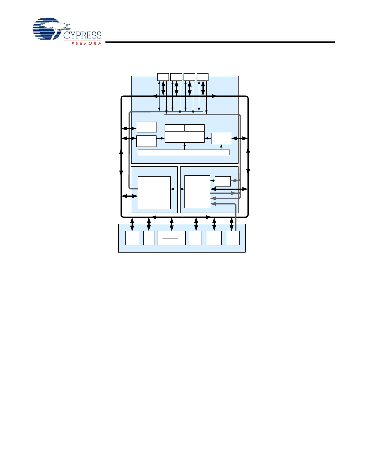
Figure 1. enCoRe III Low Voltage Block Diagram
CY7C603xx
System Bus
Global Digital
Interconnect
SRAM
512 Bytes
Interrupt
Controller
Clock Sources (Includes IMO and ILO)
DIGITAL SYSTEM
Digital
PSoC
Block
Array
Digital
Clocks
I2C
Port 3 Port 2
enCoRe II LV Core
POR and LVD
System Resets
SYSTEM RESOURCES
Port 1 Port 0
Global Analog Interconnect
SROM Flash 8K
CPU Core
(M8C)
ANALOG SYSTEM
Analog
PSoC
Block
Array
Switch
Mode
Pump
Sleep and
Watchdog
Internal
Voltage
Ref.
Analog
Ref.
Analog
Mux
Applications
•Wireless mice
• Wireless gamepads
• Wireless Presenter tools
• Wireless keypads
®
•PlayStation
2 wired gamepads
• PlayStation 2 bridges for wireless gamepads
• Applications requiring a cost effective low voltage 8-bit
microcontroller.
enCoRe III Low Voltage Functional Overview
The enCoRe III Low Voltage (enCoRe III LV) CY7C603xx
device is based on the flexible PSoC
set of peripherals is supported that can be configured as
required to match the needs of each application. Additional ly,
a fast CPU, Flash program memory, SRAM data memory, and
configurable IO are included in a range of convenient pinouts.
This architecture allows the user to create customized
peripheral configurations that match the requirements of each
individual application. Additionally, a fast CPU, Flash program
memory, SRAM data memory, and configurable IO are
included in both a 28-pin SSOP and 32-pin QFN packages.
®
architecture. A simple
enCoRe III LV architecture, as illustrated in Figure 1, is
composed of four main areas: the enCoRe III LV Core, the
System Resources, Digital System, Analog System and
System Resources. Configurable global bus resources allow
all the device resources to be combined into a complete
custom system. Each enCoRe III LV device support s a limited
set of digital and analog peripherals. Depending on the
package, up to 28 general purpose IOs (GPIOs) are also
included. The GPIOs provide access to the global digital and
analog interconnects.
enCoRe III LV Core
The enCoRe III LV core is a powerful engine that supports a
rich feature set. It encompasses SRAM for data storage, an
interrupt controller, sleep and watchdog timers, and IMO
(internal main oscillator) and ILO (internal low-speed oscillator).
The CPU core, called the M8C, is a powerful p rocessor with
speeds up to 12 MHz. The M8C is a four MIPS 8-bit Harvard
architecture microprocessor. The core includes a CPU,
memory, clocks, and configurable GPIO (General Purpose
IO).
System Resources provide additional capability, such as
digital clocks to increase flexibility, I2C functionality for implementing an I2C master, slave, MultiMaster , an internal voltage
reference that provides an absolute value of 1.3V to a number
of subsystems, a switch mode pump (SMP) that generates
Document #: 38-16018 Rev. *D Page 2 of 29
CY7C603xx
normal operating voltages off a single battery cell, and various
system resets supported by the M8C.
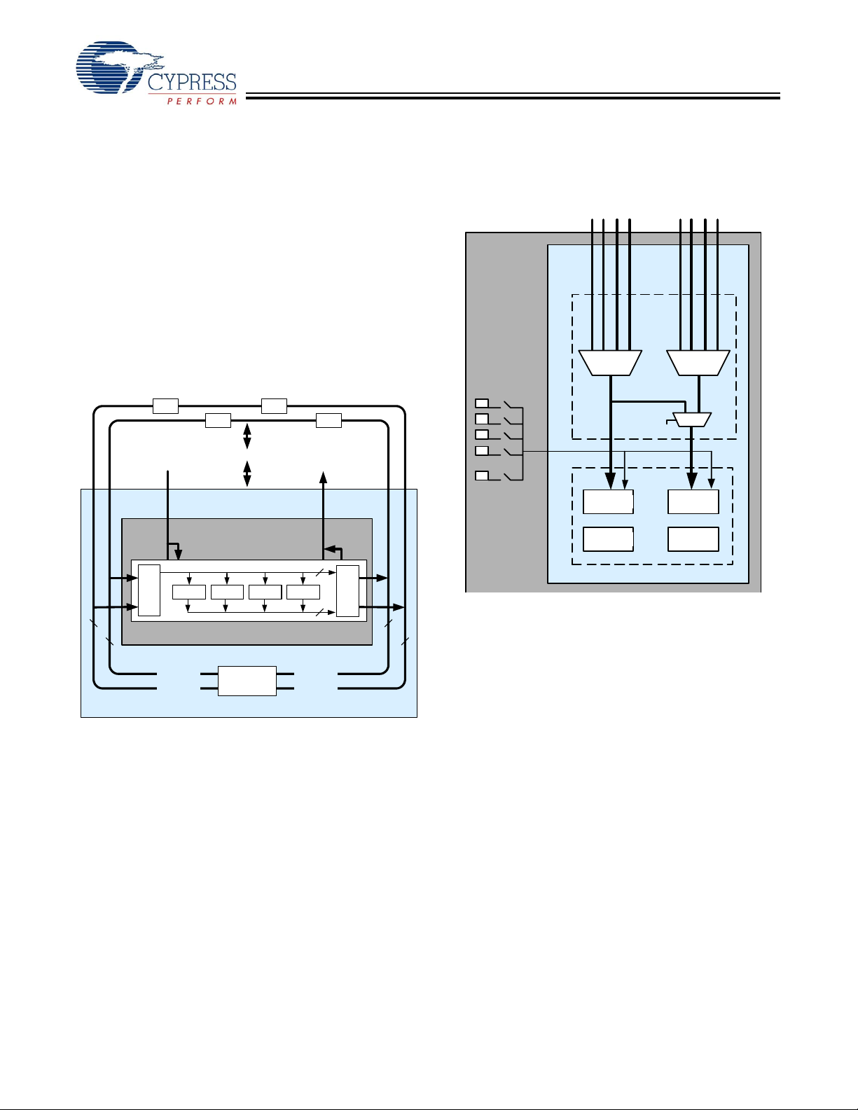
The Digital System
The Digital System is composed of 4 digital enCoRe III LV
blocks. Each block is an 8-bit resource. Digital peripheral
configurations include those listed below.
• PWM usable as Timer/Counter
• SPI master and slave
• I2C slave and multi-master
•CMP
•ADC10
• SARADC
Figure 2. Digital System Block Diagram
Port 3
Port 2
D
c
o
l
C
l
a
t
i
g
i
o
r
F
s
k
To System Bus
r
o
m
C
e
Port 1
Port 0
To Analog
System
DIGITAL SYSTEM
Digital enCoRe II LV Block Array
Row 0
Configuration
Row Output
4
Analog blocks are provided in columns of two, which includes
one CT (Continuous Time - ACE00 or ACE01) and one SC
(Switched Capacitor - ASE10 or ASE11) blocks.
Figure 3. Analog System Block Diagram
Array Input
Configuration
ACI0[1:0] ACI1[1:0]
All IO
X
X
X
X
X
ACOL1MUX
Analog Mux Bus
Array
ACE00 ACE01
ASE10 ASE11
DBB00 DBB01 DCB02 DCB03
Row Input
8
Configuration
GIE[7:0]
GIO[7:0]
Global Digital
Interconnect
4
8
GOE[7:0]
GOO[7:0]
The digital blocks can be connected to any GPIO through a
series of global buses that can route any signal to any pin. The
buses also allow for signal multiplexing and for performing
logic operations. This configurability frees your designs from
the constraints of a fixed peripheral controller.
The Analog System
The Analog System is composed of two configurable blocks.
Analog peripherals are very flexible and can be customized to
support specific application requirements. Some of the
common analog functions for this device (most available as
user modules) are listed below.
• Analog-to-digital converters (single with 8-bit resolution)
• Pin-to-pin comparators
• Single-ended comparators with absolute (1.3V) reference
• 1.3V reference (as a System Resource)
The Analog Multiplexer System
88
The Analog Mux Bus can connect to every GPIO pin. Pins can
be connected to the bus individually or in any combination.
The bus also connects to the analog system for analysis with
comparators and analog-to-digital converters. An additional
8:1 analog input multiplexer provides a second path to bring
Port 0 pins to the analog array.
Additional System Resources
System Resources, some of which have been previously
listed, provide additional capability useful to complete
systems. Additional resources include a switch mode pump,
low voltage detection, and power on reset. Brief statements
describing the merits of each system resource are presented
below.
• Digital clock dividers provide three customizable clock
frequencies for use in applications. The clocks can be
routed to both the digital and analog systems. Additional
clocks can be generated using digital blocks as clock
dividers.
• The I2C module provides 100- and 400-kHz communication
over two wires. Slave, master, and multi-master modes are
all supported.
• Low Voltage Detection (L VD) interrupts can signal the application of falling voltage levels, while the advanced POR
(Power On Reset) circuit eliminates the need for a system
supervisor.
Document #: 38-16018 Rev. *D Page 3 of 29
CY7C603xx
• An internal 1.3 voltage reference provides an absolute
reference for the analog system.
• An integrated switch mode pump (SMP) generates normal
operating voltages from a single 1.2V battery cell, providing
a low-cost boost converter.
• Versatile analog multiplexer system.
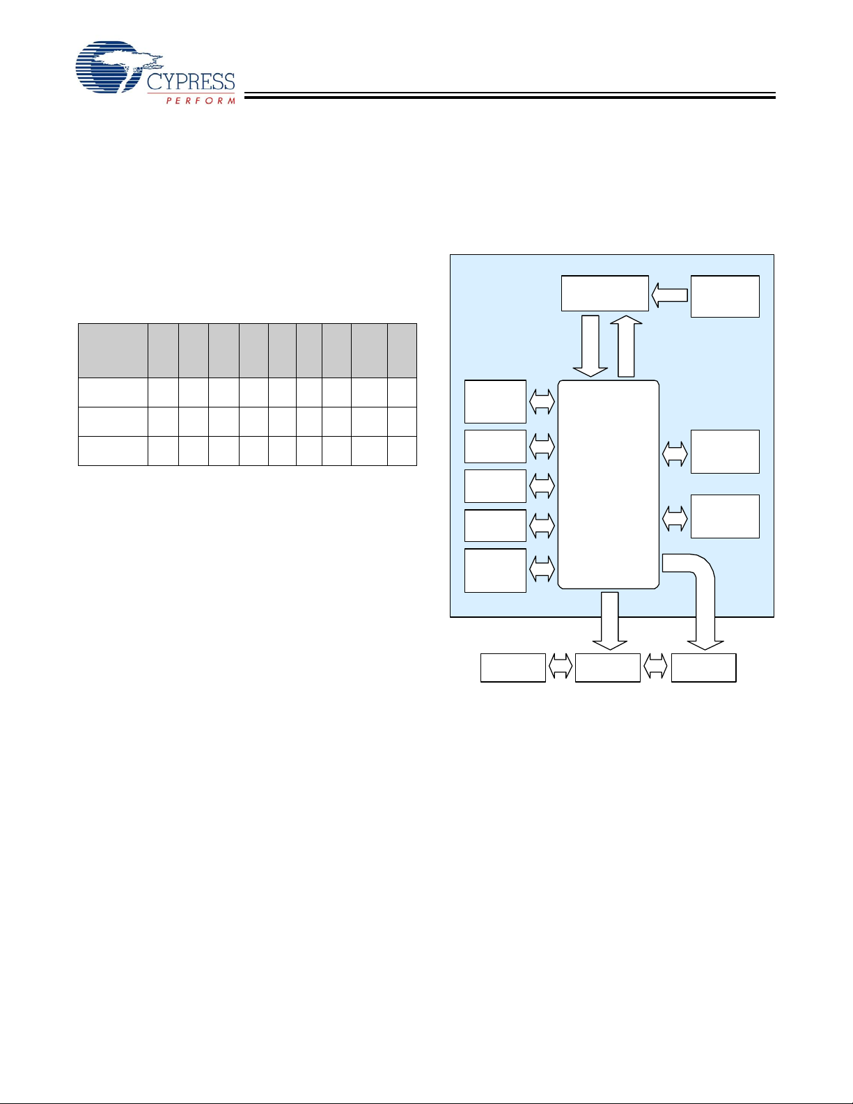
enCoRe III LV Device Characteristics
enCoRe III L V devices have four digital b locks and four analog
blocks. The following table lists the resources available for
specific enCoRe III LV devices.
Part
Number
CY7C60323
-PVXC
CY7C60323
-LFXC
CY7C60333
-LFXC
Rows
Digital IODigital
24 1 4 24 0 2 4 512
28 1 4
28 1 4
Inputs
Digital
Blocks
Analog
Analog
Analog
Outputs
Columns
28 0 2 4 512
26 0 2 4 512
Analog
Blocks
Bytes
Bytes
Bytes
SRAM
Size
Flash
8K
8K
8K
Getting Started
The quickest path to understanding the enCoRe III LV silicon
is by reading this data sheet and using the PSoC Designer
Integrated Development Environment (IDE). This data sheet
is an overview of the enCoRe III LV and presents specific pin,
register, and electrical specifications. enCoRe III LV is based
on the architecture of the CY8C21x34. For in-depth information, along with detailed programming information, refer to
the PSoC Mixed-Signal Array Technical Reference Manual,
which can be found on http://www.cypress.com/psoc.
For up-to-date Ordering, Packaging, and Electrical Specification information, refer to the latest device data sheets on the
web at http://www.cypress.com.
integrated debugger with In-Circuit Emulator, in-system
programming support, and the CYASM macro assembler for
the CPUs.
PSoC Designer also supports a high-level C language
compiler developed specifically for the devices in the family.
Figure 4. PSoC Designer Subsystems
PSoC
TM
Graphical Designer
Interface
Sensitive
Designer
Results
Size
Importable
Des ign
Databas e
Device
Databas e
Application
Databas e
Project
Databas e
User
Modules
Library
Emulation
Pod
Commands
TM
PSoC
Designer
Core
Engine
In-Circuit
Emulator
Configuration
M a nufacturing
Inf ormation
Device
Programmer
Context
Help
PSoC
Sheet
File
Development Kits
PSoC Designer Software Subsystems
Development Kits are available from the following distributors:
Digi-Key, A vnet, Arrow , and Future. The Cypress Online Store
contains development kits, C compilers, and all accessories
for enCoRe III LV development. Go to the Cypress Online
Store web site at http://www.cypress.com, click the Online
Store shopping cart icon at the bottom of the web page, and
click USB (Universal Serial Bus) to view a current list of
available items.
Development Tools
Device Editor
The device editor subsystem allows the user to select different
on-board analog and digital components called user modules
using the blocks. Examples of user modules are ADCs,
PWMs, and SPI.
PSoC Designer sets up power-on initialization tables for
selected block configurations and creates source code for an
application framework. The framework contains software to
operate the selected components and, if the project uses more
PSoC Designer is a Microsoft® Windows®-based, integrated
development environment for the enCoRe III LV. The PSoC
Designer IDE and application runs on Windows NT 4.0,
Windows 2000, Windows Millennium (Me), or Windows XP.
(Refer to the PSoC Designer Functional Flow diagram below.)
PSoC Designer helps the customer to select an operating
configuration, write application code that uses the
enCoRe III LV, and debug the application. This system
than one operating configuration, contains routines to switch
between different sets of block configurations at run time.
PSoC Designer can print out a configuration sheet for a given
project configuration for use during application p rogramming
in conjunction with the Device Data Sheet. Once the
framework is generated, the user can add application-specific
code to flesh out the framework. It is also possible to change
the selected components and regenerate the framework.
provides design database management by project, an
Document #: 38-16018 Rev. *D Page 4 of 29

CY7C603xx
Application Editor
In the Application Editor you can edit your C language and
Assembly language source code. You can also assemble,
compile, link, and build.
Assembler. The macro assembler allows the assembly code
to be merged seamlessly with C code. The link libraries
automatically use absolute addressing or can be compiled in
relative mode and linked with other software modules to get
absolute addressing.
C Language Compiler. A C language compiler is available
that supports the enCoRe III LV family of devices. Even if you
have never worked in the C language before, the product
quickly allows you to create complete C programs.
The embedded, optimizing C compiler provides all the
features of C tailored to the enCoRe III LV architecture. It
comes complete with embedded libraries providing port and
bus operations, standard keypad and display support, and
extended math functionality.
Debugger
The PSoC Designer Debugger subsystem provides hardware
in-circuit emulation, allowing the designer to test the progra m
in a physical system while providing an internal view of the
device. Debugger commands allow the designer to read the
program and read and write data memory, read and write IO
registers, read and write CPU registers, set and clear breakpoints, and provide program run, halt, and step control. The
debugger also allows the designer to create a trace buffer of
registers and memory locations of interest.
Online Help System
The online help system displays online, context-sensitive help
for the user. Designed for procedural and quick reference,
each functional subsystem has its own context-sensitive help.
This system also provides tutorials and links to FAQs and an
Online Support Forum to aid the designer in getting started.
Hardware Tools
In-Circuit Emulator
A low cost, high functionality ICE (In-Circuit Emulator) is
available for development support. This hardware has the
capability to program single devices.
The emulator consists of a base unit that connects to the PC
by way of a USB port. The base unit is universal and will
operate with enCoRe III LV, enCoRe III, and all PSoC devices.
Emulation pods for each device family are available
separately. The emulation pod takes the place of the
enCoRe III LV device in the target board and performs full
speed (12 MHz) operation.
Designing with User Modules
The development process for the enCoRe III LV device differs
from that of a traditional fixed-function microprocessor. The
configurable analog and digital hardware blocks provide a
unique flexibility that pays dividends in managing specification
change during development and by lowering inventory costs.
These configurable resources have the ability to implement a
wide variety of user-selectable functions. Each block has
several registers that determine its function and connectivity
to other blocks, multiplexers, buses and to the IO pins.
Iterative development cycles permit you to adapt the hardware
as well as the software. This substantially lowers the risk of
having to select a different part to meet the final design require-
ments.
To speed the development process, the PSoC Designer
Integrated Development Environment (IDE) provides a library
of prebuilt, pretested hardware peripheral functions, called
“User Modules.” User Modules make selecting and imple-
menting peripheral devices simple, and come in analog,
digital, and mixed signal varieties. The standard User Module
library contains seven common peripherals such as ADCs,
SPI, I2C and PWMs to configure the enCoRe III LV periph-
erals.
Each user module establishes the basic register settings that
implement the selected function. It also provides parameters
that allow you to tailor its precise configuration to your
particular application. For example, a Pulse Width Modulator
User Module configures a digital enCoRe III LV block for 8 bits
of resolution. The user module parameters permit you to
establish the pulse width and duty cycle. User modules also
provide tested software to cut your development time. The
user module application programming interface (API) provides
high-level functions to control and respond to hardware events
at run time. The API also provides optional interrupt service
routines that you can adapt as needed.
The API functions are documented in user module data sheets
that are viewed directly in the PSoC Designer IDE. These
data sheets explain the internal operation of the user module
and provide performance specifications. Each data sheet
describes the use of each user module parameter and
documents the setting of each register controlled by the user
module.
The development process starts when you open a new project
and bring up the Device Editor, a graphical user interface
(GUI) for configuring the hardware. Y ou pick the user modules
you need for your project and map them onto the
enCoRe III LV blocks with point-and-click simplicity. Next, you
build signal chains by interconnecting user modules to each
other and the IO pins. At this stage, you also configure the
clock source connections and enter parameter values directly
or by selecting values from drop-down menus. When you are
ready to test the hardware configuration or move on to devel-
oping code for the project, you perform the “Generate Appli-
cation” step. This causes PSoC Designer to generate source
code that automatically configures the device to your specifi -
cation and provides the high-level user module API functions.
Document #: 38-16018 Rev. *D Page 5 of 29
CY7C603xx
Figure 5. User Module and Source Code Development
Flows
Device Editor
User
Module
Selection
Placement
and
Parameter
-ization
Source
Code
Generator
Generate
Application
Application Editor
Project
Manager
Source
Code
Editor
Build
Manager
Build
All
Debugger
Interface
to ICE
Storage
Inspector
Event &
Breakpoint
Manager
The next step is to write your main program, and any subroutines using PSoC Designer’s Application Editor subsystem.
The Application Editor includes a Project Manager that allows
you to open the project source code files (including all
generated code files) from a hierarchal view. The source code
editor provides syntax coloring and advanced edit features for
both C and assembly language. File search capabilities
include simple string searches and recursive “grep-style”
patterns. A single mouse click invokes the Build Manager. It
employs a professional-strength “makefile” system to
automatically analyze all file dependencies and run the
compiler and assembler as necessary. Project-level options
control optimization strategies used by the compiler and linker.
Syntax errors are displayed in a console window. Double
clicking the error message takes you directly to the offending
line of source code. When all is correct, the linker builds a HEX
file image suitable for programming.
The last step in the development process takes place inside
the PSoC Designer’s Debugger subsystem. The Debugger
downloads the HEX image to the In-Circuit Emulator (ICE)
where it runs at full speed. Debugger capabilities rival those of
systems costing many times more. In addition to traditional
single-step, run-to-breakpoint and watch-variable features,
the Debugger provides a large trace buffer and allows you
define complex breakpoint events that include monitoring
address and data bus values, memory locations and external
signals.
Document Conventions
Acronyms Used
Acronym Description
AC alternating current
ADC analog-to-digital converter
API application programming interface
CPU central processing unit
CT continuous time
ECO external crystal oscillator
EEPROM el ectrically erasable programmable read-only
memory
FSR full scale range
GPIO general purpose IO
GUI graphical user interface
HBM human body model
ICE in-circuit emulator
ILO internal low speed oscillator
IMO internal main oscillator
IO input/output
IPOR imprecise power on reset
LSb least-significant bit
LVD low voltage detect
MSb most-significant bit
PC program counter
PLL phase-locked loop
POR power on reset
PPOR precision power on reset
PSoC Programmable System-on-Chip™
PWM pulse width modulator
SC switched capacitor
SRAM static random access memory
Units of Measure
A units of measure table is located in the Electrical Specifications section. Table 5 on page 13 lists all the abbreviations
used to measure the enCoRe III LV devices.
Numeric Naming
Hexidecimal numbers are represented with all letters in
uppercase with an appended lowercase ‘h’ (for example, ‘14h’
or ‘3Ah’). Hexidecimal numbers may also be represented by a
‘0x’ prefix, the C coding convention. Binary numbers have an
appended lowercase ‘b’ (e.g., 01010100b’ or ‘01000011b’).
Numbers not indicated by an ‘h’ or ‘b’ are decimal.
Document #: 38-16018 Rev. *D Page 6 of 29
CY7C603xx
Packages/Pinouts
The enCoRe III LV device is available in 28-pin SSOP and 32-pin QFN packages, which are listed and illustrated in the following
tables. Every port pin (labeled with a “P”) is capable of Digital IO and connection to the common analog bus. However, Vss, Vdd,
SMP, and XRES are not capable of Digital IO.
Table 1. 28-Pin Part Pinout (SSOP)
Pin
No.
Type
Digital Analog
Name Description
1 IO I, M P0[7] Analog column mux input.
2 IO I, M P0[5] Analog column mux input and column output.
3 IO I, M P0[3] Analog column mux input and column output,
integrating input.
4 IO I, M P0[1] Analog column mux input, integrating input.
5 IO M P2[7]
6 IO M P2[5]
7 IO I, M P2[3] Direct switched capacitor block input.
8 IO I, M P2[1] Direct switched capacitor block input.
9 Power Vss Ground connection.
10 IO M P1[7] I2C Serial Clock (SCL).
11 IO M P1[5] I2C Serial Data (SDA).
12 IO M P1[3]
13 IO M P1[1] I2C Serial Clock (SCL), ISSP-SCLK.
14 Power Vss Ground connection.
15 IO M P1[0] I2C Serial Data (SDA), ISSP-SDATA.
16 IO M P1[2]
17 IO M P1[4] Optional External Clock Input (EXTCLK).
18 IO M P1[6]
19 Input XRES Active HIGH external reset with internal pull
down.
20 IO I, M P2[0] Direct switched capacitor block input.
21 IO I, M P2[2] Direct switched capacitor block input.
22 IO M P2[4]
23 IO M P2[6]
24 IO I, M P0[0] Analog column mux input.
25 IO I, M P0[2] Analog column mux input.
26 IO I, M P0[4] Analog column mux input
27 IO I, M P0[6] Analog column mux input.
28 Power Vdd Supply voltage.
LEGEND A: Analog, I: Input, O = Output, and M = Analog Mux Input.
M, I2C S C L, P 1 [7]
M, I2C S D A , P1 [5]
M, I2C S C L, P 1 [1]
CY7C60323-PVXC Device
A, I, M, P0 [7]
A, I, M, P0 [5]
A, I, M, P0 [3]
A, I, M, P0 [1]
M, P2[7]
M, P2[5]
M, P2[3]
M, P2[1]
M, P1[3]
Vss
Vss
10
11
12
13
14
1
2
3
4
5
6
7
8
9
SSOP
Vdd
28
P0[6], A , I, M
27
P0[4], A , I, M
26
P0[2], A , I, M
25
P0[0], A , I, M
24
P2[6], M
23
P2[4], M
22
P2[2], M
21
P2[0], M
20
XRES
19
P1[6], M
18
P1[4], E X TCLK, M
17
P1[2], M
16
P1[0], I2C SDA, M
15
Document #: 38-16018 Rev. *D Page 7 of 29
32-Pin Part Pinout
Ta ble 2. 32-Pin Part Pinout (QFN*)
Pin
No.
1 IO I, M P0[1] Analog column mux input, integrating input.
2 IO M P2[7]
3 IO M P2[5]
4 IO M P2[3]
5 IO M P2[1]
6 IO M P3[3] In CY7C60323 part.
6 Power SMP Switch Mode Pump (SMP) connection to re-
7 IO M P3[1] In CY7C60323 part.
7 Power Vss Ground connection in CY7C60333 part.
8 IO M P1[7] I2C Serial Clock (SCL).
9 IO M P1[5] I2C Serial Data (SDA).
10 IO M P1[3]
11 IO M P1[1] I2C Serial Clock (SCL), ISSP-SCLK.
12 Power Vss Ground connection.
13 IO M P1[0] I2C Serial Data (SDA), ISSP-SDATA.
14 IO M P1[2]
15 IO M P1[4] Optional External Clock Input (EXTCLK).
16 IO M P1[6]
17 Input XRES Active HIGH external reset with internal pull
18 IO M P3[0]
19 IO M P3[2]
20 IO M P2[0]
21 IO M P2[2]
22 IO M P2[4]
23 IO M P2[6]
24 IO I, M P0[0] A nalog column mux input.
25 IO I, M P0[2] A nalog column mux input.
26 IO I, M P0[4] A nalog column mux input.
27 IO I, M P0[6] A nalog column mux input.
28 Power Vdd Supply voltage.
29 IO I, M P0[7] A nalog column mux input.
30 IO I, M P0[5] A nalog column mux input.
31 IO I, M P0[3] Analog column mux input, integrating input.
32 Power Vss Ground connection.
Type
Digital Analog
Name Description
quired external components in CY7C60333
part.
down.
A, I, M, P0[1]
M, P2[7]
M, P2[5]
M, P2[3]
M, P2[1]
M, P3[3]
M, P3[1]
M, I2C SCL, P1[7]
A, I, M, P0[1]
M, P2[7]
M, P2[5]
M, P2[3]
M, P2[1]
SMP
Vss
M, I2C SCL, P1[7]
CY7C603xx
CY7C60323-LFXC Device
P0[5], A, I, M
Vss
P0[3], A, I, M
P0[7], A, I, M
Vdd
P0[6], A, I, M
P0[4], A, I, M
P0[2], A, I, M
131415
M, P1[2]
M, I2C SDA, P1[0]
M, EXTCLK, P1[4 ]
Vdd
P0[6], A , I, M
131415
M, P1[2]
M, I2C SDA, P1[0]
25
24
23
22
21
20
19
18
17
16
M, P1[6]
P0[4], A , I, M
P0[2], A , I, M
25
24
23
22
21
20
19
18
17
16
P1[4]
M, P1[6]
M, EXTCLK,
32313029282726
1
2
3
4
5
6
7
8
(Top View)
9
101112
M, P1[3]
M, I2C SDA, P1[5]
QFN
Vss
M, I2C SCL, P1[1]
CY7C60333-LFXC Device
P0[5], A , I, M
Vss
P0[3], A , I, M
P0[7], A , I, M
32313029282726
1
2
3
4
5
6
7
8
(Top View)
9
101112
M, P1[3]
M, I2C SDA, P1[5]
QFN
Vss
M, I2C S CL, P1[ 1 ]
P0[0], A, I, M
P2[6], M
P2[4], M
P2[2], M
P2[0], M
P3[2], M
P3[0], M
XRES
P0[0], A, I, M
P2[6], M
P2[4], M
P2[2], M
P2[0], M
P3[2], M
P3[0], M
XRES
LEGEND A = Analog, I = Input, O = Output, and M = Analog Mux Input.
* The QFN package has a center pad that must be connected to ground (Vss).
Document #: 38-16018 Rev. *D Page 8 of 29
CY7C603xx
Register Reference
This section lists the registers of the enCoRe III LV device. For
detailed register information, reference the PSoC
Mixed-Signal Array Technical Reference Manual.
Register Conventions
The register conventions specific to this section are listed in
the following table.
Register Mapping Tables
The enCoRe III LV device has a total register address space
of 512 bytes. The register space is referred to as IO space and
is divided into two banks. The XOI bit in the Flag register
(CPU_F) determines which bank the user is currently in. When
the XOI bit is set the user is in Bank 1.
Note: In the following register mapping tables, blank fields are
Reserved and should not be accessed.
Convention Description
R Read register or bit(s)
W Write register or bit(s)
L Logical register or bit(s)
C Clearable register or bit(s)
# Access is bit specific
Table 3. Register Map 0 Table: User Space
Name
PRT0DR 00 RW 40 ASE10CR0 80 RW C0
PRT0IE 01 RW 41 81 C1
PRT0GS 02 RW 42 82 C2
PRT0DM2 03 RW 43 83 C3
PRT1DR 04 RW 44 ASE11CR0 84 RW C4
PRT1IE 05 RW 45 85 C5
PRT1GS 06 RW 46 86 C6
PRT1DM2 07 RW 47 87 C7
PRT2DR 08 RW 48 88 C8
PRT2IE 09 RW 49 89 C9
PRT2GS 0A RW 4A 8A CA
PRT2DM2 0B RW 4B 8B CB
PRT3DR 0C RW 4C 8C CC
PRT3IE 0D RW 4D 8D CD
PRT3GS 0E RW 4E 8E CE
PRT3DM2 0F RW 4F 8F CF
Blank fields are Reserved and should not be accessed. # Access is bit specific.
Addr
(0,Hex) Access Name
10 50 90 CUR_PP D0 RW
11 51 91 STK_PP D1 RW
12 52 92 D2
13 53 93 IDX_PP D3 RW
14 54 94 MVR_PP D4 RW
15 55 95 MVW_PP D5 RW
16 56 96 I2C_CFG D6 RW
17 57 97 I2C_SCR D7 #
18 58 98 I2C_DR D8 RW
19 59 99 I2C_MSCR D9 #
1A 5A 9A INT_CLR0 DA RW
1B 5B 9B INT_CLR1 DB RW
1C 5C 9C DC
1D 5D 9D INT_CLR3 DD RW
Addr
(0,Hex) Access Name
Addr
(0,Hex) Access Name
Addr
(0,Hex) Access
Document #: 38-16018 Rev. *D Page 9 of 29

CY7C603xx
Table 3. Register Map 0 Table: User Space (continued)
Addr
Name
DBB00DR0 20 # AMX_IN 60 RW A0 INT_MSK0 E0 RW
DBB00DR1 21 W AMUXCFG 61 RW A1 INT_MSK1 E1 RW
DBB00DR2 22 RW PWM_CR 62 RW A2 INT_VC E2 RC
DBB00CR0 23 # 63 A3 RES_WDT E3 W
DBB01DR0 24 # CMP_CR0 64 # A4 E4
DBB01DR1 25 W 65 A5 E5
DBB01DR2 26 RW CMP_CR1 66 RW A6 DEC_CR0 E6 RW
DBB01CR0 27 # 67 A7 DEC_CR1 E7 RW
DCB02DR0 28 # ADC0_CR 68 # A8 E8
DCB02DR1 29 W ADC1_CR 69 # A9 E9
DCB02DR2 2A RW 6A AA EA
DCB02CR0 2B # 6B AB EB
DCB03DR0 2C # TMP_DR0 6C RW AC EC
DCB03DR1 2D W TMP_DR1 6D RW AD ED
DCB03DR2 2E RW TMP_DR2 6E RW AE EE
DCB03CR0 2F # TMP_DR3 6F RW AF EF
Blank fields are Reserved and should not be accessed. # Access is bit specific.
(0,Hex)
1E 5E 9E INT_MSK3 DE RW
1F 5F 9F DF
30 70 RDI0RI B0 RW F0
31 71 RDI0SYN B1 RW F1
32 ACE00CR1 72 RW RDI0IS B2 RW F2
33 ACE00CR2 73 RW RDI0LT0 B3 RW F3
34 74 RDI0LT1 B4 RW F4
35 75 RDI0RO0 B5 RW F5
36 ACE01CR1 76 RW RDI0RO1 B6 RW F6
37 ACE01CR2 77 RW B7 CPU_F F7 RL
38 78 B8 F8
39 79 B9 F9
3A 7A BA FA
3B 7B BB FB
3C 7C BC FC
3D 7D BD DAC_D FD RW
3E 7E BE CPU_SCR1 FE #
3F 7F BF CPU_SCR0 FF #
Access Name
Addr
(0,Hex)
Access Name
Addr
(0,Hex)
Access Name
Addr
(0,Hex)
Access
Document #: 38-16018 Rev. *D Page 10 of 29
CY7C603xx
Table 4. Register Map 1 Table: Configuration Space
Name
PRT0DM0 00 RW 40 ASE10CR0 80 RW C0
PRT0DM1 01 RW 41 81 C1
PRT0IC0 02 RW 42 82 C2
PRT0IC1 03 RW 43 83 C3
PRT1DM0 04 RW 44 ASE11CR0 84 RW C4
PRT1DM1 05 RW 45 85 C5
PRT1IC0 06 RW 46 86 C6
PRT1IC1 07 RW 47 87 C7
PRT2DM0 08 RW 48 88 C8
PRT2DM1 09 RW 49 89 C9
PRT2IC0 0A RW 4A 8A CA
PRT2IC1 0B RW 4B 8B CB
PRT3DM0 0C RW 4C 8C CC
PRT3DM1 0D RW 4D 8D CD
PRT3IC0 0E RW 4E 8E CE
PRT3IC1 0F RW 4F 8F CF
DBB00FN 20 RW CLK_CR0 60 RW A0 OSC_CR0 E0 RW
DBB00IN 21 RW CLK_CR1 61 RW A1 OSC_CR1 E1 RW
DBB00OU 22 RW ABF_CR0 62 RW A2 OSC_CR2 E2 RW
DBB01FN 24 RW CMP_GO_EN 64 RW A4 VLT_CMP E4 R
DBB01IN 25 RW 65 A5 ADC0_TR E5 RW
DBB01OU 26 RW AMD_CR1 66 RW A6 ADC1_TR E6 RW
DCB02FN 28 RW 68 A8 IMO_TR E8 W
DCB02IN 29 RW 69 A9 ILO_TR E9 W
DCB02OU 2A RW 6A AA BDG_TR EA RW
Blank fields are Reserved and should not be accessed. # Access is bit specific.
Addr
(1,Hex) Access Name
10 50 90 GDI_O_IN D0 RW
11 51 91 GDI_E_IN D1 RW
12 52 92 GDI_O_OU D2 RW
13 53 93 GDI_E_OU D3 RW
14 54 94 D4
15 55 95 D5
16 56 96 D6
17 57 97 D7
18 58 98 MUX_CR0 D8 RW
19 59 99 MUX_CR1 D9 RW
1A 5A 9A MUX_CR2 DA RW
1B 5B 9B MUX_CR3 DB RW
1C 5C 9C DC
1D 5D 9D OSC_GO_EN DD RW
1E 5E 9E OSC_CR4 DE RW
1F 5F 9F OSC_CR3 DF RW
23 AMD_CR0 63 RW A3 VLT_CR E3 RW
27 ALT_CR0 67 RW A7 E7
2B CLK_CR3 6B RW AB ECO_TR EB W
Addr
(1,Hex) Access Name
Addr
(1,Hex) Access Name
Addr
(1,Hex) Access
Document #: 38-16018 Rev. *D Page 11 of 29

CY7C603xx
Table 4. Register Map 1 Table: Configuration Space (continued)
Addr
Name
DCB03FN 2C RW TMP_DR0 6C RW AC EC
DCB03IN 2D RW TMP_DR1 6D RW AD ED
DCB03OU 2E RW TMP_DR2 6E RW AE EE
Blank fields are Reserved and should not be accessed. # Access is bit specific.
(1,Hex)
2F TMP_DR3 6F RW AF EF
30 70 RDI0RI B0 RW F0
31 71 RDI0SYN B1 RW F1
32 ACE00CR1 72 RW RDI0IS B2 RW F2
33 ACE00CR2 73 RW RDI0LT0 B3 RW F3
34 74 RDI0LT1 B4 RW F4
35 75 RDI0RO0 B5 RW F5
36 ACE01CR1 76 RW RDI0RO1 B6 RW F6
37 ACE01CR2 77 RW B7 CPU_F F7 RL
38 78 B8 F8
39 79 B9 F9
3A 7A BA FLS_PR1 FA RW
3B 7B BB FB
3C 7C BC FC
3D 7D BD DAC_CR FD RW
3E 7E BE CPU_SCR1 FE #
3F 7F BF CPU_SCR0 FF #
Access Name
Addr
(1,Hex)
Access Name
Addr
(1,Hex)
Access Name
Addr
(1,Hex)
Access
Document #: 38-16018 Rev. *D Page 12 of 29

CY7C603xx
Electrical Specifications
This section presents the DC and AC electrical specifications
of the enCoRe III LV device. For the most up to date electrical
specifications, confirm that you have the most recent data
sheet by going to the web at http://www.cypress.com
Specifications are valid for 0°C ≤ T
specified, except where noted.
≤ 70°C and TJ ≤ 85°C as
A
Refer to Table 17 for the electrical specifications on the
internal main oscillator (IMO) using SLIMO mode.
Figure 6. Voltage versus CPU Frequency
3.60
V
Valid
3.00
V
Operating
Region
Vdd Voltage
2.70
V
2.40
V
93 kHz 12 MHz
3 MHz
CPU Frequency
Figure 7. IMO Frequency Trim Options
3.60 V
3.00 V
Vdd Vol ta ge
2.40 V
93 kHz 12 MHz 24 MHz
SLIMO
Mode=1
SLIMO
Mode=1
IMO Frequency
Mode=1
6 MHz
SLIMO
Mode=0
SLIMO
The allowable CPU operating region for 12 MHz has been
extended down to 2.7V from the original 3.0V design target.
The customer's application is responsible for monitoring
voltage and throttling back CPU speed in accordance with
Figure 6 when voltage approaches 2.7V. Refer to Table 15 for
LVD specifications. Note that the device does not support a
preset trip at 2.7V. To detect Vdd drop at 2.7V, an external
circuit or device such as the WirelessUSB LP - CYRF6936
must be employed; or if the design permits, the nearest LVD
trip value at 2.9V can be used.
Table 5 lists the units of measure that are used in this section.
Table 5. Units of Measure
Symbol Unit of Measure Symbol Unit of Measure
°C degree Celsius µW microwatts
dB decibels mA milliampere
fF femtofarad ms millisecond
Hz hertz mV millivolts
KB 1024 bytes nA nanoampere
Kbit 1024 bits ns nanosecond
kHz kilohertz nV nanovolts
kΩ kilohm W ohm
MHz megahertz pA picoampere
MΩ megaohm pF picofarad
µA microampere pp peak-to-peak
µF microfarad ppm parts per million
µH microhenry ps picosecond
µs microsecond sps samples per second
µV microvolts s sigma: one standard deviation
µVrms microvolts root-mean-square V volts
Document #: 38-16018 Rev. *D Page 13 of 29

CY7C603xx
Absolute Maximum Ratings
Table 6. Absolute Maximum Ratings
Parameter Description Min. Typ. Max. Unit Notes
T
STG
T
A
Vdd Supply Voltage on Vdd Relative to Vss –0.5 – 5 V
V
IO
V
IOZ
I
MIO
ESD Electro Static Discharge Voltage 2000 – – V Human Body Model ESD.
LU Latch-up Current – – 200 mA
Operating Temperature
Table 7. Operating Temperature
Parameter Description Min. Typ. Max. Unit Notes
T
A
T
J
Storage Temperature –40 – +90 °C Higher storage temperatures will
reduce data retention time.
Ambient Temperature with Power Applied 0 – +70 °C
DC Input Voltage Vss – 0.5 – Vdd + 0.5 V
DC Voltage Applied to Tri-state Vss – 0.5 – Vdd + 0.5 V
Maximum Current into any Port Pin –25 – +25 mA
Ambient Temperature 0 – +70 °C
Junction Temperature 0 – +85 °C The temperature rise from
ambient to junction is package
specific. See “Thermal Imped-
ances” on page 27. The user must
limit the power consumption to
comply with this requirement.
DC Electrical Characteristics
DC Chip-Level Specifications
Table 8 lists guaranteed maximum and minimum specifications for the voltage and temperature ranges: 3.0V to 3.6V and
0°C<
TA< 70°C, or 2.4V to 3.0V and 0°C < TA < 70°C, respectively. Typical parameters apply to 3.3V, or 2.7V at 25°C and are
for design guidance only.
Table 8. DC Chip-Level Specifications
Parameter Description Min. Typ. Max. Unit Notes
Vdd Supply Voltage 2.40 – 3.6 V See Table 15 on page 18.
I
DD3
Supply Current, IMO = 6 MHz using SLIMO
mode.
– 1.2 2 mA Co nd itions are Vdd = 3.3V,
T
= 25°C, CPU = 3 MHz, clock
A
doubler disabled. VC1 = 375 kHz,
VC2 = 23.4 kHz, VC3 = 0.091 kHz.
I
DD27
Supply Current, IMO = 6 MHz using SLIMO
mode.
– 1.1 1.5 mA Condit i o ns are Vdd = 2.55V,
= 25°C, CPU = 3 MHz, clock
T
A
doubler disabled. VC1 = 375 kHz,
VC2 = 23.4 kHz, VC3 = 0.091 kHz.
I
SB27
Sleep (Mode) Current with POR, LVD, Sleep
Timer , WDT, and internal slow oscillator active.
– 2.6 4. µA Vdd = 2.55V, 0°C < TA < 40°C.
Mid temperature range.
I
SB
V
REF
V
REF27
AGND Analog Ground V
Sleep (Mode) Current with POR, LVD, Sleep
– 2.8 5 µA Vdd = 3.3V, 0°C < TA < 70°C.
Timer, WDT, and internal slow oscillator active.
Reference Voltage (Bandgap) 1.28 1.30 1.32 V T rimmed for appropriate Vdd.
Vdd = 3.0V to 3.6V.
Reference Voltage (Bandgap) 1.16 1.30 1.33 V T rimmed for appropriate Vdd.
Vdd = 2.4V to 3.0V.
–
REF
0.003
V
REFVREF
0.003
+
V
Document #: 38-16018 Rev. *D Page 14 of 29

CY7C603xx
DC General Purpose IO Specifications
The following tables list guaranteed maximum and minimum specifications for the voltage and temperature ranges: 3.0V to 3.6V
and 0°C <
are for design guidance only.
Table 9. 3.3V DC GPIO Specifications
Parameter Description Min. Typ. Max. Unit Notes
R
PU
R
PD
V
OH
V
OL
V
IL
V
IH
V
H
I
IL
C
IN
C
OUT
TA < 70°C, or 2.4V to 3.0V and 0°C < TA < 70°C, respectively. T ypical parameters apply to 3.3V, and 2.7V at 25°C and
Pull-up Resistor 4 5.6 8 kΩ
Pull-down Resistor 4 5.6 8 kΩ
High Output Level Vdd –
––VIOH = 3 mA, VDD > 3.0V
1.0
Low Output Level – – 0.75 V IOL = 10 mA, VDD > 3.0V
Input Low Level – – 0.8 V Vdd = 3.0 to 3.6.
Input High Level 2.1 – V Vdd = 3.0 to 3.6.
Input Hysteresis – 60 – mV
Input Leakage (Absolute Value) – 1 – nA Gross tested to 1 µA.
Capacitive Load on Pins as Input – 3.5 10 pF Package and pin dependent. Temp = 25°C.
Capacitive Load on Pins as Output – 3.5 10 pF Package and pin dependent. Temp = 25°C.
Table 10.2.7V DC GPIO Specifications
Parameter Description Min. Typ. Max. Unit Notes
R
PU
R
PD
V
OH
Pull-up Resistor 4 5.6 8 kΩ
Pull-down Resistor 4 5.6 8 kΩ
High Output Level Vdd –
––VIOH = 2.5 mA (6.25 Typ ) , VDD = 2.4 to 3.0V
0.4
(16 mA maximum, 50 mA Typ combined I
budget).
V
V
V
V
I
C
C
OL
IL
IH
H
IL
IN
OUT
Low Output Level – – 0.75 V IOL = 10 mA, V
maximum combined I
= 2.4 to 3.0V (90 mA
DD
OL
Input Low Level – – 0.75 V Vdd = 2.4 to 3.0.
Input High Level 2.0 – – V Vdd = 2.4 to 3.0.
Input Hysteresis – 90 – mV
Input Leakage (Absolute Value) – 1 – nA Gross tested to 1 µA.
Capacitive Load on Pins as Input – 3.5 10 pF Package and pin dependent. Temp = 25°C.
Capacitive Load on Pins as Output – 3.5 10 pF Package and pin dependent. Temp = 25°C.
budget).
OH
Document #: 38-16018 Rev. *D Page 15 of 29

CY7C603xx
DC Operational Amplifier Specifications
The following tables list guaranteed maximum and minimum specifications for the voltage and temperature ranges: 3.0V to 3.6V
and 0°C <
are for design guidance only.
Table 11.3.3V DC Operational Amplifier Specifications
Parameter Description Min. Typ. Max. Unit Notes
V
OSOA
TCV
I
EBOA
C
INOA
V
CMOA
G
OLOA
I
SOA
Table 12.2.7V DC Operational Amplifier Specifications
Parameter Description Min. Typ. Max. Unit Notes
V
OSOA
TCV
I
EBOA
C
INOA
V
CMOA
G
OLOA
I
SOA
TA < 70°C, or 2.4V to 3.0V and 0°C < TA < 70°C, respectively. Typical parameters apply to 3.3V , or 2.7V at 25°C and
Input Offset Voltage (absolute value) – 2.5 15 mV
OSOA
Average Input Offset Voltage Drift – 10 – µV/°C
[1]
Input Leakage Current (Port 0 Analog Pins) – 200 – pA Gross tested to 1 µA.
Input Capacitance (Port 0 Analog Pins) – 4.5 9.5 pF Package and pin dependent.
Temp = 25°C.
Common Mode Voltage Range 0 – Vdd – 1 V
Open Loop Gain – 80 – dB
Amplifier Supply Current – 10 30 µA
Note
1. Atypical behavior: I
of Port 0 Pin 0 is below 1 nA at 25°C; 50 nA over temperature. Use Port 0 Pins 1–7 for the lowest leakage of 200 nA.
EBOA
Document #: 38-16018 Rev. *D Page 16 of 29

CY7C603xx
DC Switch Mode Pump Specifications
Table 13 lists guaranteed maximum and minimum specifications fo r the voltage and temperature ranges: 3.0V to 3.6V and
0°C<
TA < 70°C, or 2.4V to 3.0V and 0°C < TA < 70°C, respectively. Typical parameters apply to 3.3V, or 2.7V at 25°C and are
for design guidance only.
Table 13.DC Switch Mode Pump (SMP) Specifications
Parameter Description Min. Typ. Max. Unit Notes
V
PUMP3V
3.3V Output Voltage from Pump 3 .0 0 3.25 3.60 V Configuration of footnote.
Average, neglecting ripple.
SMP trip voltage is set to 3.25V.
V
PUMP2V
2.6V Output Voltage from Pump 2 .4 5 2.55 2.80 V Configuration of footnote.
Average, neglecting ripple.
SMP trip voltage is set to 2.55V.
I
PUMP
V
BAT3V
V
BAT2V
V
BATSTART
∆V
PUMP_Line
Available Output Current
8
–
V
BAT
V
BAT
= 1.5V, V
= 1.3V, V
PUMP
PUMP
= 3.25V
= 2.55V
8
–
–
–
Input Voltage Range from Battery 1.0 – 3.3 V Configuration of footnote.
Input Voltage Range from Battery 1.0 – 2.8 V Configuration of footnote.
Minimum Input Volt age from Battery to
1.2 – – V Configuration of footnote.
Start Pum p
Line Regulation (over Vi range) – 5 – %VOConfiguration of footnote.
Configuration of footnote.
mA
SMP trip voltage is set to 3.25V.
mA
SMP trip voltage is set to 2.55V.
SMP trip voltage is set to 3.25V.
SMP trip voltage is set to 2.55V.
TA < 100. 1.25V at TA = –40°C.
0°C <
Value for PUMP Trip” specified by the
VM[2:0] setting in the DC POR and LVD
Specification, Table 15 on page 18.
∆V
PUMP_Load
Load Regulation – 5 – %VOConfiguration of footnote.
Value for PUMP Trip” specified by the
VM[2:0] setting in the DC POR and LVD
Specification, Table 15 on page 18.
∆V
PUMP_Ripple
E
3
E
2
F
PUMP
DC
PUMP
Output Voltage Ripple (depends on
– 100 – mVpp Configuration of footnote.
cap/load)
Efficiency 35 50 – % Configuration of footnote.
SMP trip voltage is set to 3.25V.
Efficiency 35 80 – % For I load = 1 mA, V
= 1.3V, 10 µH inductor, 1 µF
V
BAT
capacitor, and Schottky diode.
Switching Frequency – 1.3 – MHz
Switching Duty Cycle – 50 – %
PUMP
[2]
[2]
[2]
[2]
[2]
[2]
[2]
[2]
[2]
[2]
= 2.55V,
VO is the “Vdd
VO is the “Vdd
Load is 5 mA.
Load is 5 mA.
Figure 8. Basic Switch Mode Pump Circuit
D
1
Vdd
L
1
+
V
BAT
Battery
Note
2. L
= 2 µH inductor, C1 = 10 µF capacitor, D1 = Schottky diode. See Figure 8.
1
enCoRe III LV
SMP
Vss
V
PUMP
C
1
Document #: 38-16018 Rev. *D Page 17 of 29

CY7C603xx
DC Analog Mux Bus Specifications
The following table lists guaranteed maximum and minimum specifications for the voltage and temperature ranges: 3.0V to 3.6V
and 0°C <
are for design guidance only.
Table 14.DC Analog Mux Bus Specifications
Parameter Description Min. Typ. Max. Unit Notes
R
SW
R
VDD
DC POR and LVD Specifications
The following table lists guaranteed maximum and minimum specifications for the voltage and temperature ranges: 3.0V to 3.6V
and 0°C <
are for design guidance only.
Table 15.DC POR and LVD Specifications
Parameter Description Min. Typ. Max. Unit Notes
V
PPOR0
V
PPOR1
V
LVD0
V
LVD1
V
LVD2
V
LVD37
V
PUMP0
V
PUMP1
V
PUMP2
V
PUMP3
TA < 70°C, or 2.4V to 3.0V and 0°C < TA < 70°C, respectively. Typical parameters apply to 3.3V , or 2.7V at 25°C and
Switch Resistance to Common Analog Bus – – 400
800
Ω
Ω
Vdd > 2.7V
Vdd < 2.7V
2.4V <
Resistance of Initialization Switch to Vdd – – 800 Ω
TA < 70°C, or 2.4V to 3.0V and 00°C < TA < 70°C, respectively. Typical parameters apply to 3.3V, or 2.7V at 25°C and
Vdd Value for PPOR Trip
PORLEV[1:0] = 00b
PORLEV[1:0] = 01b –
2.36
2.82
2.40
2.95
Vdd must be greater than or equal to
V
2.5V during startup, reset from the
V
XRES pin, or reset from Watchdog.
Vdd Value for LVD Trip
VM[2:0] = 000b 2.40 2.45 2.51
VM[2:0] = 001b 2.85 2.92 2.99
[3]
[4]
V
V
VM[2:0] = 010b 2.95 3.02 3.09 V
VM[2:0] = 011b 3.06 3.13 3.20 V
Vdd Value for PUMP Trip
VM[2:0] = 000b 2.45 2.55 2.62
[5]
V
VM[2:0] = 001b 2.96 3.02 3.09 V
VM[2:0] = 010b 3.03 3.10 3.16 V
VM[2:0] = 011b 3.18 3.25 3.32
[6]
V
Notes
3. Always greater than 50 mV above VPPOR (PORLEV = 00) for falling supply.
4. Always greater than 50 mV above VPPOR (PORLEV = 01) for falling supply.
5. Always greater than 50 mV above VLVD0.
6. Always greater than 50 mV above VLVD3.
Document #: 38-16018 Rev. *D Page 18 of 29

CY7C603xx
DC Programming Specifications
The following table lists guaranteed maximum and minimum specifications for the voltage and temperature ranges: 3.0V to 3.6V
and 0°C <
are for design guidance only.
Table 16.DC Programming Specifications
Parameter Description Min. Typ. Max. Unit Notes
Vdd
I
DDP
V
ILP
V
IHP
I
ILP
I
IHP
V
OLV
V
OHV
Flash
Flash
Flash
TA < 70°C, or 2.4V to 3.0V and 0°C < TA < 70°C, respectively. Typical parameters apply to 3.3V , or 2.7V at 25°C and
IWRITE
Supply Voltage for Flash Write Operations 2.70 – – V
Supply Current During Programming or Verify – 5 25 mA
Input Low Voltage During Programming or Verify – – 0.8 V
Input High Voltage During Programming or Verify 2.1 – – V
Input Current when Applying Vilp to P1[0] or P1[1]
During Programming or Verify
Input Current when Applying Vihp to P1[0] or P1[1]
During Programming or Verify
Output Low Voltage During Programming or Verify – – Vss +
– – 0.2 mA Driving internal pull down
resistor.
– – 1.5 mA Driving internal pull down
resistor.
V
0.75
Output High Voltage During Programming or Verify Vdd – 1.0 – Vdd V
Flash Endurance (per block) 50,000 – – – Erase/write cycles per block.
ENPB
Flash Endurance (total)
ENT
Flash Data Retention 10 – – Years
DR
[7]
1,800,000 – – – Erase/write cycles.
Note
7. A maximum of 36 x 50,000 block endurance cycles is allowed. This may be balanced between operations on 36x1 blocks of 50,000 maximum cycles each, 36 x2
blocks of 25,000 maximum cycles each, or 36x4 blocks of 12,500 maximum cycles ea ch (to limit the total number of cycles to 36x50,000 and that no single bl ock
ever sees more than 50,000 cycl e s) .
Document #: 38-16018 Rev. *D Page 19 of 29

CY7C603xx
AC Electrical Characteristics
AC Chip-Level Specifications
The following tables list guaranteed maximum and minimum specifications for the voltage and temperature ranges: 3.0V to 3.6V
and 0°C <
are for design guidance only.
Table 17.3.3V AC Chip-Level Specifications
Parameter Description Min. Typ. Max. Unit Notes
F
IMO24
F
IMO6
F
CPU2
F
BLK33
F
32K1
Jitter32k 32 kHz RMS Period Jitter – 100 200 ns
Jitter32k 32 kHz Peak-to-Peak Pe riod Jitter – 1400 –
T
XRST
DC24M 24 MHz Duty Cycle 40 50 60 %
Step24M 24 MHz Trim Step Size – 50 – kHz
Fout48M 48 MHz Output Frequency 46.8 48.0 49.2
Jitter24M1 24 MHz Peak-to-Peak Period Jitter (IMO) – 600 ps
F
MAX
T
RAMP
Table 18.2.7V AC Chip-Level Specifications
TA < 70°C, or 2.4V to 3.0V and 0°C < TA < 70°C, respectively. Typical parameters apply to 3.3V , or 2.7V at 25°C and
Internal Main Oscillator Frequency for
24 MHz
23.4 24 24.6
[8, 9]
MHz Trimmed for 3.3V operation using factory
trim values. See Figure 7 on page 13.
SLIMO mode = 0.
Internal Main Oscillator Frequency for
6MHz
5.75 6 6.35
[8, 9]
MHz Trimmed for 3.3V operation using factory
trim values. See Figure 7 on page 13.
SLIMO mode = 1.
CPU Frequency (3.3V Nominal) 0.93 12 12.3
Digital Block Frequency (3.3V Nominal) 0 24 24.6
[8, 9]
[8, 10]
MHz
MHz
Internal Low Speed Oscillator Frequency 15 32 64 kHz
External Reset Pulse Width 10 – – µs
[9]
MHz Trimmed. Using factory trim values.
Maximum frequency of signal on row
– – 12.3 MHz
input or row output.
Supply Ramp Time 0 – – µs
Parameter Description Min. Typ. Max. Unit Notes
F
IMO12
Internal Main Oscillator Frequency for 12 MHz 11.5 12012.7
[8, 11]
MHz Trimmed for 2.7V operation
using factory trim values.
See Figure 7 on page 13.
SLIMO mode = 1.
F
IMO6
Internal Main Oscillator Frequency for 6 MHz 5.75 6 6.35
[8, 11]
MHz Trimmed for 2.7V operation
using factory trim values.
See Figure 7 on page 13.
SLIMO mode = 1.
F
CPU1
F
BLK27
F
32K1
CPU Frequency (2.7V Nominal) 0.093 3 3.15
Digital Block Frequency (2.7V Nominal) 0 12 12.5
Internal Low Speed Oscillator Frequency 8 32 96 kHz
[8, 11]
[8, 11]
MHz 24 MHz only for SLIMO
mode = 0.
MHz Refer to the AC Digital Block
Specifications below.
Jitter32k 32 kHz RMS Period Jitter – 150 200 ns
Jitter32k 32 kHz Peak-to-Peak Period Jitter – 1400 –
T
XRST
F
MAX
T
RAMP
Notes
8. Accuracy derived from Internal Main Oscillator with appropriate trim for Vdd range.
9. 3.0V < Vdd < 3.6V.
10.See the individual user module data sheets for information on maximum frequencies for user modules.
11.2.4V < Vdd < 3.0V.
External Reset Pulse Width 10 – – µs
Maximum frequency of signal on row input or
– – 12.3 MHz
row output.
Supply Ramp Time 0 – – µs
Document #: 38-16018 Rev. *D Page 20 of 29

CY7C603xx
Figure 9. 24-MHz Period Jitter (IMO) Timing Diagram
Jitter24M1
F
24M
Figure 10. 32-kHz Period Jitter (ILO) Timing Diagram
Jitter32k
F
32K1
AC General Purpose IO Specifications
The following tables list guaranteed maximum and minimum specifications for the voltage and temperature ranges: 3.0V to 3.6V
and 0°C <
are for design guidance only.
Table 19.3.3V AC GPIO Specifications
Parameter Description Min. Typ. Max. Unit Notes
F
GPIO
TRiseS Rise Time, Slow Strong Mode, Cload = 50 pF 7 27 – ns Vdd = 3 to 3.6V, 10%–90%
TFallS Fall Time, Slow Strong Mode, Cload = 50 pF 7 22 – ns Vdd = 3 to 3.6V, 10%–90%
TA < 70°C, or 2.4V to 3.0V and 0°C < TA < 70°C, respectively. Typical parameters apply to 3.3V , or 2.7V at 25°C and
GPIO Operating Frequency 0 – 12 MHz Normal Strong Mode
Table 20.2.7V AC GPIO Specifications
Parameter Description Min. Typ. Max. Unit Notes
F
GPIO
TRiseF Rise Time, Normal Strong Mode, Cload = 50 pF
TFallF Fall Time, Normal Strong Mode, Cload = 50 pF
TRiseS Rise Time, Slow Strong Mode, Cload = 50 pF
TFallS Fall Time, Slow Strong Mode, Cload = 50 pF
GPIO Operating Frequency 0 – 3 MHz Normal Strong Mode
6 – 50 ns Vdd = 2.4 to 3.0V, 10%–90%
6 – 50 ns Vdd = 2.4 to 3.0V, 10%–90%
18 40 120 ns Vdd = 2.4 to 3.0V, 10%–90%
18 40 120 ns Vdd = 2.4 to 3.0V, 10%–90%
Figure 11. GPI O Timing Diagram
90%
GPIO
Pin
Output
Voltage
10%
TRiseF
TRiseS
TFallF
TFallS
Document #: 38-16018 Rev. *D Page 21 of 29

CY7C603xx
AC Operational Amplifier Specifications
The following table lists guaranteed maximum and minimum specifications for the voltage and temperature ranges: 3.0V to 3.6V
and 0°C <
are for design guidance only.
Table 21.AC Operational Amplifier Specifications
Parameter Description Min. Typ. Max. Unit Notes
T
COMP
AC Analog Mux Bus Specifications
The following table lists guaranteed maximum and minimum specifications for the voltage and temperature ranges: 3.0V to 3.6V
and 0°C <
are for design guidance only.
Table 22.AC Analog Mux Bus Specifications
Parameter Description Min. Typ. Max. Unit Notes
F
SW
TA < 70°C, or 2.4V to 3.0V and 0°C < TA < 70°C, respectively. Typical parameters apply to 3.3V , or 2.7V at 25°C and
Comparator Mode Respon se Time, 50 m V Overdrive 100
200
TA < 70°C, or 2.4V to 3.0V and 0°C < TA < 70°C, respectively. Typical parameters apply to 3.3V , or 2.7V at 25°C and
nsnsVdd > 3.0V.
2.4V < Vcc < 3.0V.
Switch Rate – – 3.17 MHz
AC Digital Block Specifications
The following tables list guaranteed maximum and minimum specifications for the voltage and temperature ranges: 3.0V to 3.6V
and 0°C <
are for design guidance only.
Table 23.3.3V AC Digital Block S pecifications
Function Description Min. Typ. Max. Unit Notes
All Functions Maximum Block Clocking Frequency (< 3.6V) 24.6 MHz 3.0V < Vdd < 3.6V.
Timer/
Counter/
PWM
Dead Band Kill Pulse Width:
SPIM Maximum Input Clock Frequency – – 8.2 MHz Maximum data rate at 4.1 MHz
SPIS Maximum Input Clock Frequency – – 4.1 MHz
Transmitter Maximum Input Clock Frequency – – 24.6 MHz Maximum data rate at 3.08 MHz
Receiver Maximum Input Clock Frequency – – 24.6 MHz Maximum data rate at 3.08 MHz
TA < 70°C, or 2.4V to 3.0V and 0°C < TA < 70°C, respectively. Typical parameters apply to 3.3V , or 2.7V at 25°C and
Enable Pulse Width 50
Maximum Frequency – – 24.6 MHz
Asynchronous Restart Mode 20 – – ns
Synchronous Restart Mode 50 – – ns
Disable Mode 50 – – ns
Maximum Frequency – – 49.2 MHz 4.75V < Vdd < 5.25V.
Width of SS_ Negated Between Transmissions 50 – – ns
[12]
– – ns
due to 2 x over clocking.
due to 8 x over clocking.
due to 8 x over clocking.
Note
12.50 ns minimum input pulse width is based on the input synchronizers running at 12 MHz (84 ns nominal period).
Document #: 38-16018 Rev. *D Page 22 of 29

CY7C603xx
AC External Clock Specifications
Table 24.2.7V AC Digital Block S pecifications
Function Description Min. Typ. Max. Unit Notes
All Functions Maximum Block Clocking Frequency 12.7 MHz 2.4V < Vdd < 3.0V.
Timer/
Counter/
PWM
Dead Band Kill Pulse Width:
SPIM Maximum Input Clock Frequency – – 6.35 MHz Maximum data rate at 3.17 MHz due
SPIS Maximum Input Clock Frequency – – 4.1 MHz
Transmitter Maximum Input Clock Frequency – – 12.7 MHz Maximum data rate at 1.59 MHz due
Receiver Maximum Input Clock Frequency – – 12.7 MHz Maximum data rate at 1.59 MHz due
Enable Pulse Width 100 – – ns
Maximum Frequency – – 12.7 MHz
Asynchronous Restart Mode 20 – – ns
Synchronous Restart Mode 100 – – ns
Disable Mode 100 – – ns
Maximum Frequency – – 12.7 MHz
to 2 x over clocking.
Width of SS_ Negated Between Transmissions 100 – – ns
to 8 x over clocking.
to 8 x over clocking.
The following tables list guaranteed maximum and minimum specifications for the voltage and temperature ranges: 3.0V to 3.6V
and 0°C <
Table 25.3.3V AC External Clock Specifications
Parameter Description Min. Typ. Max. Unit Notes
F
OSCEXT
F
OSCEXT
– High Period with CPU Clock divide by 1 41.7
– Low Period with CPU Clock divide by 1 41.7
– Power Up IMO to Switch 150
TA < 70°C, respectively. Typical parameters apply to 3.3V, or 2.7V at 25°C and are for design guidance only.
Frequency with CPU Clock divide by 1 0.093 – 12.3 MHz Maximum CPU frequency is 12 MHz at 3.3V.
With the CPU clock divider set to 1, the external
clock must adhere to the maximum frequency
and duty cycle requirements.
Frequency with CPU Clock divide by 2 or
greater
0.186 – 24.6 MHz If the frequency of the external clock is greater
than 12 MHz, the CPU clock divider must be
set to 2 or greater. In this case, the CPU clock
divider will ensure that the fifty percent duty
cycle requirement is met.
– 5300 ns
– –ns
– – µs
Document #: 38-16018 Rev. *D Page 23 of 29
CY7C603xx
Table 26.2.7V AC External Clock Specifications
Parameter Description Min. Typ. Max. Unit Notes
F
OSCEXT
F
OSCEXT
– High Period with CPU Clock divide by 1 160 – 5300 ns
– Low Period with CPU Clock divide by 1 160
– Power Up IMO to Switch 150
AC Programming Specifications
The following table lists guaranteed maximum and minimum specifications for the voltage and temperature ranges: 3.0V to 3.6V
and 0°C <
Table 27.AC Programming Specifications
Parameter Description Min. Typ. Max. Unit Notes
T
RSCLK
T
FSCLK
T
SSCLK
T
HSCLK
F
SCLK
T
ERASEB
T
WRITE
T
DSCLK3
T
DSCLK2
Frequency with CPU Clock divide by 1 0.093 –3.080MHz Maximum CPU frequency is 3 MHz at 2.7V.
With the CPU clock divider set to 1, the
external clock must adhere to the maximum
frequency and duty cycle requirements.
Frequency with CPU Clock divide by 2 or
greater
0.186 – 6.35 MHz If the frequency of the external clock is
greater than 3 MHz, the CPU clock divider
must be set to 2 or greater. In this case, the
CPU clock divider will ensure that the fifty
percent duty cycle requirement is met.
– –ns
– – µs
TA < 70°C, respectively. Typical parameters apply to 3.3V, or 2.7V at 25°C and are for design guidance only.
Rise Time of SCLK 1 – 20 ns
Fall Time of SCLK 1 – 20 ns
Data Set up Time to Falling Edge of SCLK 40 – – ns
Data Hold Time from Falling Edge of SCLK 40 – – ns
Frequency of SCLK 0 – 8 MHz
Flash Erase Time (Block) – 15 – ms
Flash Block Write Time – 30 – ms
Data Out Delay from Falling Edge of SCLK – – 50 ns 3.0 ≤ Vdd ≤ 3.6
Data Out Delay from Falling Edge of SCLK – – 70 ns 2.4 ≤ Vdd ≤ 3.0
Document #: 38-16018 Rev. *D Page 24 of 29

CY7C603xx
2
C Specifications
AC I
The following tables list guaranteed maximum and minimum specifications for the voltage and temperature ranges: 3.0V to 3.6V
and 0°C <
are for design guidance only.
Table 28.AC Characteristics of the I2C SDA and SCL Pins for Vdd > 3.0V
Parameter Description
F
SCLI2C
T
HDSTAI2C
T
LOWI2C
T
HIGHI2C
T
SUSTAI2C
T
HDDATI2C
T
SUDATI2C
T
SUSTOI2C
T
BUFI2C
T
SPI2C
TA < 70°C, or 2.4V to 3.0V and 0°C < TA < 70°C, respectively. Typical parameters apply to 3.3V , or 2.7V at 25°C and
Standard Mode Fast Mode
Min. Max. Min. Max.
Unit Notes
SCL Clock Frequency 0 100 0 400 kHz
Hold Time (repeated) ST AR T Condition. After
4.0 –0.6– µs
this period, the first clock pulse is generated.
LOW Period of the SCL Clock 4.7 –1.3– µs
HIGH Period of the SCL Clock 4.0 –0.6– µs
Set-up Time for a Repeated ST ART Condition 4.7 –0.6– µs
Data Hold Time 0 –0– µs
Data Set-up Time 250 –100
[13]
–ns
Set-up Time for STOP Condition 4.0 –0.6– µs
Bus Free Time Between a STOP and START
4.7 –1.3– µs
Condition
Pulse Width of spikes are suppressed by the
– –050ns
input filter.
Table 29.2.7V AC Characteristics of the I2C SDA and SCL Pins (Fast Mode not Supported)
Parameter Description
F
SCLI2C
T
HDSTAI2C
T
LOWI2C
T
HIGHI2C
T
SUSTAI2C
T
HDDATI2C
T
SUDATI2C
T
SUSTOI2C
T
BUFI2C
T
SPI2C
SCL Clock Frequency 0 100 – – kHz
Hold Time (repeated) ST ART Condition. After
this period, the first clock pulse is generated.
LOW Period of the SCL Clock 4.7 – – – µs
HIGH Period of the SCL Clock 4.0 – – – µs
Set-up Time for a Repeated ST AR T Condition 4.7 – – – µs
Data Hold Time 0 – – – µs
Data Set-up Time 250 – – –ns
Set-up Time for STOP Condition 4.0 – – – µs
Bus Free Time Between a STOP and START
Condition
Pulse Width of spikes are suppressed by the
input filter.
Standard Mode Fast Mode
Min. Max. Min. Max.
4.0 – – – µs
4.7 ––– µs
– –––ns
Unit Notes
Note
13.A Fast-Mode I2C-bus device can be used in a Standard-Mode I2C-bus system, but the requirement t
be the case if the device does not stretch the LOW period of the SCL signal. If such device does stretch the LOW period of the SCL signal, it must output the
next data bit to the SDA line t
rmax
+ t
= 1000 + 250 = 1250 ns (according to the Standard-Mode I2C-bus specification) before the SCL line is released.
SU;DAT
> 250 ns must then be met. This will automatically
SU;DAT
Document #: 38-16018 Rev. *D Page 25 of 29
Figure 12. Definition for Timing for Fast/Standard Mode on the I
2
C Bus
CY7C603xx
SDA
T
LOWI2C
T
SUDATI2C
T
HDSTAI2C
T
SPI2C
T
BUFI2C
SCL
S
T
HDSTAI2C
T
HDDATI2C
T
HIGHI2C
T
SUSTAI2C
Sr SP
T
SUSTOI2C
Packaging Information
This section illustrates the packaging specifications for the CY7C603xx device, along with the thermal impedances fo r each
package.
Important Note Emulation tools may require a larger area on the target PCB than the chip’s footprint. For a detailed description
of the emulation tools’ dimensions, refer to the document titled PSoC Emulator Pod Dimensions at
http://www.cypress.com/support/link.cfm?mr=poddim.
Packaging Dimensions
Figure 13. 28-Lead (210-Mil) SSOP
51-85079-*C
Document #: 38-16018 Rev. *D Page 26 of 29
Figure 14. 32-Lead QFN (5 x 5 mm)
CY7C603xx
0.50 DIA.
DIMENSIONS IN mm MIN.
C
4.90
5.10
4.65
4.85
N
1
2
TOP VIEW
4.65
4.85
4.90
5.10
0.93 MAX.
0.80 MAX.
0°-12°
SIDE VIEW
0.05
0.05 MAX.
0.20 REF.
3.70
0.30-0.50
C
SEATING
PLANE
3.70
0.23±0.05
0.50
3.50
BOTTOM VIEW
JEDEC # MO-220
Package Weight: 0.054 grams
MAX.
N
51-85188-*A
PIN1 ID
0.20 R.
0.45
1
2
3.50
0.42±0.18
(4X)
Important Note For information on the preferred dimensions for mounting QFN packages, see the following Application Note at
http://www.amkor.com/products/notes_papers/MLFAppNote.pdf.
Thermal Impedances Solder Reflow Peak Temperature
Table 30.Thermal Impedances per Package
Package Typical θ
* Typical θ
JA
28 SSOP 96 °C/W 39 °C/W
32 QFN 22 °C/W 12 °C/W
* TJ = TA + Power x θ
JA
JC
Following is the minimum solder reflow peak temperature to
achieve good solderability.
Ta ble 31.Solder Reflow Peak Temperature
Package
Minimum Peak
T emperature*
Maximum Peak
T emperature
28 SSOP 240°C 260°C
32 QFN 240°C 260°C
*Higher temperatures may be required based on the solder
melting point. Typical temperatures for solder are 220±5°C
with Sn-Pb or 245±5°C with Sn-Ag-Cu paste. Refer to the
solder manufacturer specifications.
Document #: 38-16018 Rev. *D Page 27 of 29

CY7C603xx
Ordering Information
The following table lists the CY7C603xx device’s key package features and ordering codes.
Table 32.CY7C603xx Device Key Features and Ordering Information
Ordering
Part Number
CY7C60323-PVXC 8K 512 No 24 28-SSOP
CY7C60323-PVXCT 8K 512 No 24 28-SSOP Tape and Reel
CY7C60323-LFXC 8K 512 No 28 32-QFN
CY7C60323-LFXCT 8K 512 No 28 32-QFN Tape and Reel
CY7C60333-LFXC 8K 512 Yes 26 32-QFN
CY7C60333-LFXCT 8K 512 Yes 26 32-QFN Tape and Reel
PlayStation is a registered trademark of Sony. Microsoft and Windows are registered trademarks of Microsoft Corporation.
Purchase of I2C components from Cypress or one of its sublicensed Associated Companies conveys a license under the Philips
I2C Patent Rights to use these components in an I2C system, provided that the system conforms to the I2C Standard Specification
as defined by Philips.
PSoC is a registered trademark and enCoRe and Programmable System-on-Chip are trademarks of Cypress Semiconductor
Corporation. All products and company names mentioned in this document may be the trademarks of their respective holders.
Flash Size RAM Size SMP I/O Package Type
Document #: 38-16018 Rev. *D Page 28 of 29
© Cypress Semiconductor Corporation, 2006. The information contained herein is subject to change without notice. Cypress Semiconductor Corporation assumes no responsibility for the use
of any circuitry other than circuitry embodied in a Cypress product. Nor does it convey or imply any license under patent or other rights. Cypress products are not warranted nor intended to be
used for medical, life support, life saving, critical control or safety applications, unless pursuant to an express written agreement with Cypress . Furthermore, Cypress does no t authorize its
products for use as critical components in life-support systems where a malfunction or failure may reasonably be expected to result in significant injury to the user. The inclusion of Cypress
products in life-support systems application implies that the manufacturer assumes all risk of such use and in doing so indemnifies Cypress against all charges.
CY7C603xx
Document History Page
Description Title: CY7C603xx, enCoRe™ III Low Voltage
Document Number: 38-16018
REV. ECN NO. Issue Date
** 339394 See ECN BON New Advance Data Sheet
*A 399556 See ECN BHA Changed from Advance Information to Preliminary.
*B 461240 See ECN TYJ Modified Figure 6 to include 2.7V Vdd at 12-MHz operation
*C 470485 See ECN TYJ Corrected part numbers in section 4 to match with part numbers in Ordering
*D 513713 See KKVTMP Change title from Wireless enCoRe II to enCoRe III Low Voltage
Orig. of
Change
Description of Change
Changed data sheet format.
Removed CY7C604xx.
Information. From CY7C60323-28PVXC, CY7C60323-56LFXC and
CY7C60333-56LFXC to CY7C60323-PVXC, CY7C60323-LFXC and
CY7C60333-LFXC respectively
Changed from Preliminary to final data sheet
Applied new template formatting
Document #: 38-16018 Rev. *D Page 29 of 29
 Loading...