

CYPRESS CY7C4255, CY7C4265 User Manual
8K/16Kx18 Deep Sync FIFOs
fax id: 5413
CY7C4255
CY7C4265
PRELIMINARY
1CY7C42 65
查询2SC3133供应商查询2SC3133供应商
Features
• High-speed, low-power, first-in first-out (FIFO)
memories
• 8K x 18 (CY7C4255)
• 16K x 18 (CY7C4265)
• 0.5 micron CMOS for optimum speed/power
• High-speed 100-MHz operation (10 ns read/write cycle
times)
• Low power — I
=45 mA
CC
• Fully asynchronous and simultaneous read and write
operation
• Empty , Full, Half Full, and programmable Almost Empty
and Almost Full status flags
• T TL com p atib le
• Retransmit function
• Output Enable (OE
) pins
• Independent read and write enable pins
• Center power and ground pins for reduced noise
• Supports free-running 50% duty cycle clock inputs
• Width Expansion Capability
• Depth Expansion Capability
• 64-pin PLCC and 64-pin TQFP
• Pin-compatible density upgrade to CY7C42X5 family
• Pin-compatible density upgrade to
IDT72205/15/25/35/45
Functional Description
The CY7C4255/65 are high-speed, low-power, first-in first-out
(FIFO) memories with clocked read and write interfaces. All
D
0– 17
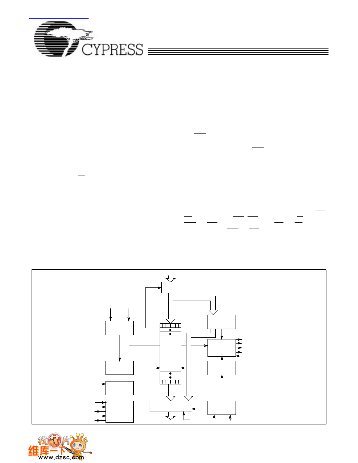
Logic Block Diagram
INPUT
REGISTER
are 18 bits wide and are pin/functionally compatible to the
CY7C42X5 Synchronous FIFO family. The CY7C4255/65 can
be cascaded to increa se FIFO depth. Programmable features
include Almost Full/Almost Empty flags. These FIFOs provide
solutions for a wide variety of data buffering needs, including
high-speed data acquisition, multiprocessor interfaces, and communications buffering.
These FIFOs have 18-bit input and output ports that are controlled by separate clo ck and enable signals. The input port is
controlled by a free-running clock (WCLK) and a write enable
pin (WEN
When WEN
edge of the WCLK signal. While WEN
).
is asserted, data is written into the FIFO on t he risi ng
is held active, data is continually written into the FIFO on each cycle. The output port is controlled
in a similar manner by a free-running read clock (RCLK) and a read
enable pin (REN
enable pin (OE
). In addition, the C Y 7C4255/65 have an output
). The read and write clocks may be tied together for
single-clock operation or the two clocks may be run independently for
asynchronous read/write applications. Clock fr equencies up to 100
MHz are achievable.
Retransmit and Synchronous Almost Full/Almost Empty flag
features are available on these devices.
Depth expansion is possible using the cascade input (WXI
RXI
), cascade output (WXO, RXO), and First Load ( FL) pins. T he
WXO
and RXO pins are connected to the WXI and RXI pins of the
next device, and the WXO
connected to the WXI
the first device is tied to V
es should be tied to V
and RXO pins of the last device should be
and RXI pins of the first device. The FL pin of
and the FL pin of all the remaining devic-
SS
.
CC
,
WENWCLK
FLAG
PROGRAM
REGISTER
FLAG
LOGIC
READ
POINTER
READ
CONTROL
RCLK
REN
FF
EF
PAE
PAF
SMODE
4255–1
RS
FL/RT
WXI
WXO/HF
RXI
RXO
WRITE
CONTROL
WRITE
POINTER
RESET
LOGIC
EXPANSION
LOGIC
RAM
ARRAY
8K x 18
16K x 18
THREE–STATE
OUTPUTREGISTER
Q
0– 17
OE
Cypress Semiconductor Corporation • 3901 North First Street • San Jose • CA 95134 • 408-943-2600
July 1995 – Revised November 1996
CY7C4255
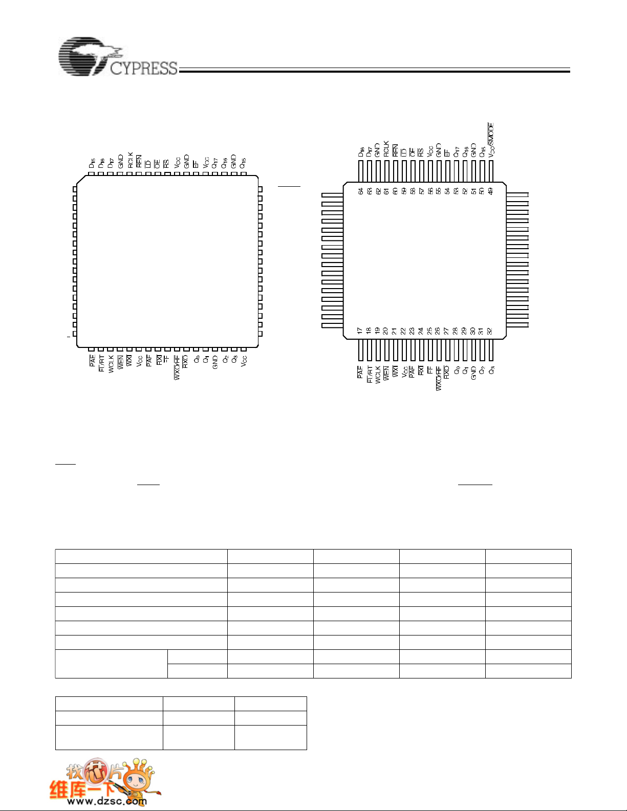
Pin Configurations
D
D
D
D
D
V
GND
D
CC
D
D
D
D
D
D
D
D
D
14
13
12
11
10
9
8
7
6
5
4
3
2
1
0
987 6
10
11
12
13
14
15
16
17
18
19
20
21
22
23
24
25
26
2728 2930
5 4 3 2 1 68 66 65 64 63 62 61
CY7C4255
CY7C4265
3132 33 34 35 36 37 38 3940 4142 43
PLCC
Top View
67
PRELIMINARY
VCC/SMODE
60
Q
59
14
Q
58
13
GND
57
Q
56
12
Q
55
11
V
54
CC
Q
53
10
Q
52
9
GND
51
Q
50
8
49
Q
7
V
48
CC
Q
47
6
Q
46
5
45
GND
Q
44
4
4255–2
CY7C4265
TQFP
Top View
D
15
D
14
D
13
D
12
D
11
D
10
D
9
D
8
D
7
D
6
D
5
D
4
D
3
D
2
D
1
D
0
1
2
3
4
5
6
7
8
9
10
11
12
13
14
15
16
CY7C4255
CY7C4265
48
47
46
45
44
43
42
41
40
39
38
37
36
35
34
33
Q
Q
GND
Q
Q
V
Q
Q
GND
Q
Q
Q
Q
GND
Q
V
4255–3
14
13
12
11
CC
10
9
8
7
6
5
4
CC
Functional Description (continued)
The Empty and Full flags are synchronous, i.e., they change
state relative to either the read clock (RCLK) or the write clock
The CY7C4255/65 provides five status pins. These pins are decoded to determine one of five states: Empty, Almost Empty, Half Full,
Almost Full, and Full (see
WXO
pin. This flag is valid in the stand-alone and width-expansion
Table 2
). The Half Full flag shares the
configurations. In the depth expansion, this pin provides
the expansion out (WXO
) information that is used to signal
the next FIFO when it will b e activate d.
(WCLK). When entering or exiting the Empty states, the flag is
updated exclusively by the RCLK. The flag denoting Full states
is updated exclusively by WCLK. The synchronous flag archi-
tecture guarantees that the flags will remain valid from one
clock cycle to the next. The Almost Empty/Almost Full flags
become synchronous if the VCC/S M O D E
is tied to VSS. All
configurations are fabricated using an advanced 0.5µ
CMOS technology. Input ESD protection is greater than
2001V, and la tch- up is pr even ted by t he use of guard rings .
Selection G uide
7C4255/65–10 7C4255/65–15 7C4255/65–25 7C4255/65–35
Maximum Frequency (MHz) 100 66.7 40 28.6
Maximum Access Time (ns) 8 10 15 20
Minimum Cycle Time (ns) 10 15 25 35
Minimum Data or Enable Set-Up (ns) 3 4 6 7
Minimum Data or Enable Hold (ns) 0.5 1 1 2
Maximum Flag Delay (ns) 8 10 15 20
Active Power Supply
Current (I
CC1
) (mA)
Density 8K x 18 16K x 18
Package 64-pin
Commercial 45 45 45 45
Industrial 50 50 50 50
CY7C4255 CY7C4265
64-pin
PLCC,TQFP
PLCC,TQFP
2
CY7C4255
PRELIMINARY
CY7C4265
Pin Definitions
Signal Name Description I/O Function
D
0 –17
Q
0–17
WEN Write Enable I Enables the WCLK input
REN Read Enable I Enables the RCLK input
WCLK Write Clock I The rising edge clocks data into the FIFO when WEN is LOW and the FIFO is not
RCLK Read Clock I The rising edge clocks data out of the FIFO when REN is LOW and the FIFO is not
WXO/HF Write Expansion
EF Empty Flag O When EF is LOW, the FIFO is empty. EF is synchronized to RCLK.
FF Full Flag O When FF is LOW, the F IF O is f u ll. FF is synchronized to WCLK.
PAE Programmable
PAF Programmable
LD Load I When LD is L O W, D
FL/RT First Load/
WXI Write Expansion
RXI Read Expansion
RXO Read Expansion
RS Reset I Resets device to empty condition. A reset is required before an initial read or write
OE Output Enable I When OE is LOW, the FIFO’s data outputs drive the bus to which they are con-
VCC/SMODE Synchronous
Data Inputs I Data inputs for an 18-bit bus
Data Outputs O Data outputs for an 18-bit bus
Full. When LD
is asserted, WCLK writes data into the programmable flag-offset
register.
Empty. When LD
is asserted, RCLK reads data out of the programmable flag-off-
set register.
O Dual-Mode Pin:
Out/Half Full Flag
Single device or width expansion – Half Full status flag.
Cascaded – Write Expansion Out signal, connected to WXI
O When PAE is LOW, the FIFO is almost empty based on the almost-empty offset
Almost Empty
value p rogrammed i nto the FIFO. P AE
to V
; it is synchronized to RCLK when VCC/SMODE is tied to VSS.
CC
O When PAF is LOW, the FIFO is almost full based on the almost full offset value
Almost Full
programmed into the FIFO. PAF
V
; it is synchronized to WCLK when VCC/SMODE is tied to VSS.
CC
(Q
ble-flag -o ffs et r e gis te r.
0 – 17
I Dual-Mode Pin:
Retransmit
Cascaded – The first device in the daisy chain will have FL
devices will hav e FL
to V
on all devices.
SS
Not Cascaded – Tied to V
mode by strobing RT.
tied to VCC. In standard mode or width exp ans ion, FL is tied
SS
I Cascaded – Connected to WXO of previous device.
Input
Not Cascaded – Tied to V
SS
I Cascaded – Connected to RXO of previous device.
Input
Not Cascaded – Tied to V
SS
O Cascaded – Connected to RXI of next device.
Output
operation after power-up.
nected. If O E
is HIGH, the FIFO’s outputs are in High Z (high-impedance) state.
I Dual-Mode Pin
Almost Empty/
Almost Full Flags
Asynchronous Almost Empty/Almost Full flags – tied to V
Synchronous Almost Empty/Almost Full flags – tied to V
(Almost Empty synchr on iz e d to R C L K , A lm o st F u ll synchro n iz ed to WC L K .)
of next device.
is asynchronous when VCC/SMODE is tied
is asynchronous when VCC/SMODE is tied to
) are written (read) into (from) the programma-
0 – 17
tied to VSS; all other
. Retransmit function is also available in stand-alone
.
.
.
CC
.
SS
3
CY7C4255
PRELIMINARY
Maximum Ratings
(Above which the useful life may be impaired. For user guidelines, not tested.)
Storage Temperature ................................–65
Ambient Temperature with
Power Applied............................................–55
Supply Voltage to Ground Potential............... –0.5V to +7.0V
DC Voltage Applied to Outputs
in High Z State ...............................................–0.5V to +7.0V
DC Input Voltage...........................................−0.5V to V
Electrical Characteristics Over the Operating Range
°C to +1 50° C
°C to +125 ° C
+0.5V
cc
Output Current into Outputs (LOW)............................. 20 mA
Static Discharge Voltage...........................................>2001V
(per MIL–STD–883, Method 3015)
Latch-Up Current .....................................................>200 mA
Operating Range
Ambient
Range
Commercial 0°C to +70°C 5V ± 10%
Industrial
[2]
[1]
Temperature
–40°C to +85°C 5V ± 10%
CY7C4265
V
CC
7C42X5–10 7C42X5–15 7C42X5–25 7C42X5– 35
Parameter Description Test Conditions Min. Max. Min. Max. Min. Max. Min. Max. Unit
V
V
V
V
I
IX
I
OZL
I
OZH
I
CC1
I
CC2
OH
OL
IH
IL
[3]
[4]
[5]
[6]
Output HIGH Voltage VCC = Min .,
I
= –2.0 mA
OH
Output LOW Voltage VCC = Min .,
I
= 8.0 mA
OL
Input HIGH Voltage 2.0 V
2.4 2.4 2.4 2.4 V
0.4 0.4 0.4 0.4 V
CC
2.0 V
CC
2.0 V
CC
2.0 V
CC
Input LOW Voltage –0.5 0.8 –0.5 0.8 –0.5 0.8 –0.5 0.8 V
Input Leakage
Current
Output OFF,
High Z Current
Active Power Supply
Current
Average Standby
Current
V
= Max. –10 +10 –10 +10 –10 +10 –10 +10 µA
CC
OE > VIH,
V
< VO < V
SS
CC
–10 +10 –10 +10 –10 +10 –10 +10 µA
Com’l 45 45 45 45 mA
Ind 50 50 50 50 mA
Com’l 10 10 10 10 mA
Ind 15 15 15 15 mA
V
Capacitance
[7,8]
Paramet er Description Test Conditions Max. Unit
C
IN
C
OUT
Notes:
1. T
is the “instant on” case temperature.
A
2. See the last page of this specification for Group A subgroup testing information.
3. The VIH and VIL specifications apply for all inputs except WXI, RXI. The WXI, RXI pin is not a TTL input. It is connected to either RXO, WXO of the
previous device or VSS.
4. The V
5. Input signals switch from 0V to 3V with a rise/fall time of less than 3 ns, clocks and clock enables switch at 20MHz, while data inputs switch at 10MHz. Outputs
6. All inputs = VCC – 0.2V, except RCLK and WCLK (which are switching at frequency = 20 MHz), and FL/RT which is at Vss. All outputs are unloaded.
7. Tested initially and after any design changes that may affect these parameters.
8. Tested initially and after any process changes that may affect these parameters.
and VIL specifications apply for all inputs except WXI, RXI. The WXI, RXI pin is not a TTL input. It is connected to either RXO, WXO of the
IH
previous device or V
ar e u n loa d ed. Icc1 (t ypica l) = (25mA+(freq-20MHz)*(1.0mA/MHz))
Input Capacitance TA = 25°C, f = 1 MH z ,
V
= 5.0 V
Output Capacitance 7 pF
SS.
CC
5 pF
4
CY7C4255
CY7C4265
90%
10%
ns
4255–5
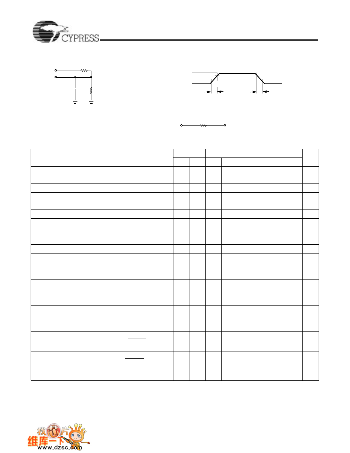
AC Test Loads and Waveforms
R1 1.1K
5V
OUTPUT
INCLUDING
C
JIG AND
SCOPE
L
Ω
R2
680Ω
4255–4
PRELIMINARY
[9, 10]
3.0V
GND
≤ 3ns ≤ 3
Equivalent to: THÉ VENIN EQUIVALENT
410Ω
OUTPUT 1.91V
ALL INPUT PULSES
90%
10%
Switching Characteristics Over the Operating Range
7C42X5–10 7C42X5–15 7C42X5–25 7C42X5–35
Parameter Description Min. Max. Min. Max. Min. Max. Min. Max. Unit
t
S
t
A
t
CLK
t
CLKH
t
CLKL
t
DS
t
DH
t
ENS
t
ENH
t
RS
t
RSR
t
RSF
t
PRT
t
RTR
t
OLZ
t
OE
t
OHZ
t
WFF
t
REF
t
PAFasynch
t
P AFsyn ch
t
P A Easyn ch
Notes:
9. C
L
10. CL = 5 pF for t
11. Pulse widths less than minimum values are not allowed.
12. Values guaranteed by design, not currently tested.
13. t
PAFasynch
Clock Cycle Frequency 100 66.7 40 28.6 MHz
Data Access Time 2 8 2 10 2 15 2 20 ns
Clock Cycle Time 10 15 25 35 ns
Clock HIGH Time 4.5 6 10 14 ns
Clock LOW Time 4.5 6 10 14 ns
Data Set-Up Time 3 4 6 7 ns
Data Hold Time 0.5 1 1 2 ns
Enable Set-Up Time 3 4 6 7 ns
Enable Hold Time 0.5 1 1 2 ns
Reset Pulse Width
[11]
10 15 25 35 ns
Reset Recovery Time 8 10 15 20 ns
Reset to Flag and Output Time 10 15 25 35 ns
Retransmit Pulse Width 30 35 45 55 ns
Retransmit Recovery Time 60 65 75 85 ns
Output Enable to Output in Low Z
[12]
0 0 0 0 ns
Output Enable to Output Valid 3 7 3 8 3 12 3 15 ns
Output Enable to Output in High Z
[12]
3 7 3 8 3 12 3 15 ns
Write Clock to Full Flag 8 10 15 20 ns
Read Clock to Empty Flag 8 10 15 20 ns
Clock to Programmable Almost-Full Flag
[13]
12 16 20 25 ns
(Asynchronous mode, VCC/SMODE tied to
V
)
CC
Clock to Programmable Almost-Full Flag
(Synchronous mode, V
/SMODE tied to VSS)
CC
Clock to Programmable Almost-Empty Flag
[13]
8 10 15 20 ns
12 16 20 25 ns
(Asynchronous mode, VCC/SMODE tied to VCC)
= 30 pF for all AC parameters except for t
, t
.
OHZ
, after program register write will not be valid until 5 ns + t
PAEa syn ch
OHZ
.
.
PAF (E)
5
CY7C4255
PRELIMINARY
CY7C4265
Switching Characteristics Over the Operating Range (continued)
7C42X5–10 7C42X5–15 7C42X5–25 7C42X5–35
Parameter Descriptio n Min. Max. Min. Max. Min. Max. Min. Max. Unit
t
PAEsynch
t
HF
t
XO
t
XI
t
XIS
t
SKEW1
t
SKEW2
t
SKEW3
Clock to Programmable Almost-Full Flag
(Synchronous mode, V
Clock to Half-Full Flag 12 16 20 25 ns
Clock to Expansion Out 6 10 15 20 ns
Expansion in Pulse Width 4.5 6.5 10 14 ns
Expansion in Set-Up Time 4 5 10 15 ns
Skew Time between Read Clock and Write
Clock for Full Flag
Skew Time between Read Clock and Write
Clock for Empty Flag
Skew Time between Read Clock and Write
Clock for Programmable Almost Empty and Programmable Almost Full Flags (Synchronous
Mode only)
/SMODE tied to VSS)
CC
10 15 18 20 ns
8 10 15 20 ns
5 6 10 12 ns
5 6 10 12 ns
6
 Loading...