

8K/16Kx18 Deep Sync FIFOs
fax id: 5413
CY7C4255
CY7C4265
PRELIMINARY
1CY7C42 65
查询2SC3133供应商查询2SC3133供应商
Features
• High-speed, low-power, first-in first-out (FIFO)
memories
• 8K x 18 (CY7C4255)
• 16K x 18 (CY7C4265)
• 0.5 micron CMOS for optimum speed/power
• High-speed 100-MHz operation (10 ns read/write cycle
times)
• Low power — I
=45 mA
CC
• Fully asynchronous and simultaneous read and write
operation
• Empty , Full, Half Full, and programmable Almost Empty
and Almost Full status flags
• T TL com p atib le
• Retransmit function
• Output Enable (OE
) pins
• Independent read and write enable pins
• Center power and ground pins for reduced noise
• Supports free-running 50% duty cycle clock inputs
• Width Expansion Capability
• Depth Expansion Capability
• 64-pin PLCC and 64-pin TQFP
• Pin-compatible density upgrade to CY7C42X5 family
• Pin-compatible density upgrade to
IDT72205/15/25/35/45
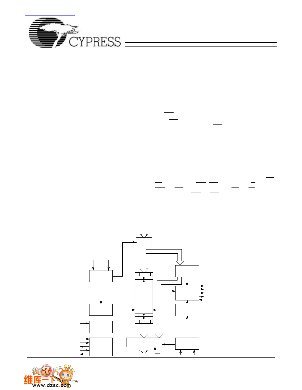
Functional Description
The CY7C4255/65 are high-speed, low-power, first-in first-out
(FIFO) memories with clocked read and write interfaces. All
D
0– 17
Logic Block Diagram
INPUT
REGISTER
are 18 bits wide and are pin/functionally compatible to the
CY7C42X5 Synchronous FIFO family. The CY7C4255/65 can
be cascaded to increa se FIFO depth. Programmable features
include Almost Full/Almost Empty flags. These FIFOs provide
solutions for a wide variety of data buffering needs, including
high-speed data acquisition, multiprocessor interfaces, and communications buffering.
These FIFOs have 18-bit input and output ports that are controlled by separate clo ck and enable signals. The input port is
controlled by a free-running clock (WCLK) and a write enable
pin (WEN
When WEN
edge of the WCLK signal. While WEN
).
is asserted, data is written into the FIFO on t he risi ng
is held active, data is continually written into the FIFO on each cycle. The output port is controlled
in a similar manner by a free-running read clock (RCLK) and a read
enable pin (REN
enable pin (OE
). In addition, the C Y 7C4255/65 have an output
). The read and write clocks may be tied together for
single-clock operation or the two clocks may be run independently for
asynchronous read/write applications. Clock fr equencies up to 100
MHz are achievable.
Retransmit and Synchronous Almost Full/Almost Empty flag
features are available on these devices.
Depth expansion is possible using the cascade input (WXI
RXI
), cascade output (WXO, RXO), and First Load ( FL) pins. T he
WXO
and RXO pins are connected to the WXI and RXI pins of the
next device, and the WXO
connected to the WXI
the first device is tied to V
es should be tied to V
and RXO pins of the last device should be
and RXI pins of the first device. The FL pin of
and the FL pin of all the remaining devic-
SS
.
CC
,
WENWCLK
FLAG
PROGRAM
REGISTER
FLAG
LOGIC
READ
POINTER
READ
CONTROL
RCLK
REN
FF
EF
PAE
PAF
SMODE
4255–1
RS
FL/RT
WXI
WXO/HF
RXI
RXO
WRITE
CONTROL
WRITE
POINTER
RESET
LOGIC
EXPANSION
LOGIC
RAM
ARRAY
8K x 18
16K x 18
THREE–STATE
OUTPUTREGISTER
Q
0– 17
OE
Cypress Semiconductor Corporation • 3901 North First Street • San Jose • CA 95134 • 408-943-2600
July 1995 – Revised November 1996
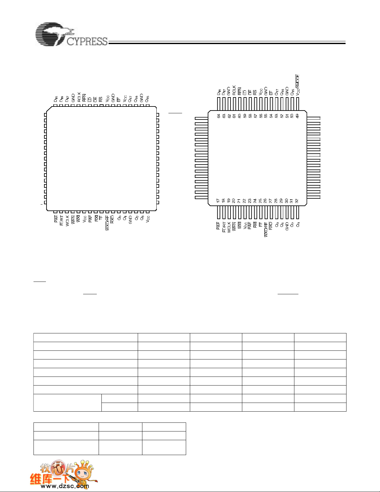
CY7C4255
Pin Configurations
D
D
D
D
D
V
GND
D
CC
D
D
D
D
D
D
D
D
D
14
13
12
11
10
9
8
7
6
5
4
3
2
1
0
987 6
10
11
12
13
14
15
16
17
18
19
20
21
22
23
24
25
26
2728 2930
5 4 3 2 1 68 66 65 64 63 62 61
CY7C4255
CY7C4265
3132 33 34 35 36 37 38 3940 4142 43
PLCC
Top View
67
PRELIMINARY
VCC/SMODE
60
Q
59
14
Q
58
13
GND
57
Q
56
12
Q
55
11
V
54
CC
Q
53
10
Q
52
9
GND
51
Q
50
8
49
Q
7
V
48
CC
Q
47
6
Q
46
5
45
GND
Q
44
4
4255–2
CY7C4265
TQFP
Top View
D
15
D
14
D
13
D
12
D
11
D
10
D
9
D
8
D
7
D
6
D
5
D
4
D
3
D
2
D
1
D
0
1
2
3
4
5
6
7
8
9
10
11
12
13
14
15
16
CY7C4255
CY7C4265
48
47
46
45
44
43
42
41
40
39
38
37
36
35
34
33
Q
Q
GND
Q
Q
V
Q
Q
GND
Q
Q
Q
Q
GND
Q
V
4255–3
14
13
12
11
CC
10
9
8
7
6
5
4
CC
Functional Description (continued)
The Empty and Full flags are synchronous, i.e., they change
state relative to either the read clock (RCLK) or the write clock
The CY7C4255/65 provides five status pins. These pins are decoded to determine one of five states: Empty, Almost Empty, Half Full,
Almost Full, and Full (see
WXO
pin. This flag is valid in the stand-alone and width-expansion
Table 2
). The Half Full flag shares the
configurations. In the depth expansion, this pin provides
the expansion out (WXO
) information that is used to signal
the next FIFO when it will b e activate d.
(WCLK). When entering or exiting the Empty states, the flag is
updated exclusively by the RCLK. The flag denoting Full states
is updated exclusively by WCLK. The synchronous flag archi-
tecture guarantees that the flags will remain valid from one
clock cycle to the next. The Almost Empty/Almost Full flags
become synchronous if the VCC/S M O D E
is tied to VSS. All
configurations are fabricated using an advanced 0.5µ
CMOS technology. Input ESD protection is greater than
2001V, and la tch- up is pr even ted by t he use of guard rings .
Selection G uide
7C4255/65–10 7C4255/65–15 7C4255/65–25 7C4255/65–35
Maximum Frequency (MHz) 100 66.7 40 28.6
Maximum Access Time (ns) 8 10 15 20
Minimum Cycle Time (ns) 10 15 25 35
Minimum Data or Enable Set-Up (ns) 3 4 6 7
Minimum Data or Enable Hold (ns) 0.5 1 1 2
Maximum Flag Delay (ns) 8 10 15 20
Active Power Supply
Current (I
CC1
) (mA)
Density 8K x 18 16K x 18
Package 64-pin
Commercial 45 45 45 45
Industrial 50 50 50 50
CY7C4255 CY7C4265
64-pin
PLCC,TQFP
PLCC,TQFP
2
CY7C4255
PRELIMINARY
CY7C4265
Pin Definitions
Signal Name Description I/O Function
D
0 –17
Q
0–17
WEN Write Enable I Enables the WCLK input
REN Read Enable I Enables the RCLK input
WCLK Write Clock I The rising edge clocks data into the FIFO when WEN is LOW and the FIFO is not
RCLK Read Clock I The rising edge clocks data out of the FIFO when REN is LOW and the FIFO is not
WXO/HF Write Expansion
EF Empty Flag O When EF is LOW, the FIFO is empty. EF is synchronized to RCLK.
FF Full Flag O When FF is LOW, the F IF O is f u ll. FF is synchronized to WCLK.
PAE Programmable
PAF Programmable
LD Load I When LD is L O W, D
FL/RT First Load/
WXI Write Expansion
RXI Read Expansion
RXO Read Expansion
RS Reset I Resets device to empty condition. A reset is required before an initial read or write
OE Output Enable I When OE is LOW, the FIFO’s data outputs drive the bus to which they are con-
VCC/SMODE Synchronous
Data Inputs I Data inputs for an 18-bit bus
Data Outputs O Data outputs for an 18-bit bus
Full. When LD
is asserted, WCLK writes data into the programmable flag-offset
register.
Empty. When LD
is asserted, RCLK reads data out of the programmable flag-off-
set register.
O Dual-Mode Pin:
Out/Half Full Flag
Single device or width expansion – Half Full status flag.
Cascaded – Write Expansion Out signal, connected to WXI
O When PAE is LOW, the FIFO is almost empty based on the almost-empty offset
Almost Empty
value p rogrammed i nto the FIFO. P AE
to V
; it is synchronized to RCLK when VCC/SMODE is tied to VSS.
CC
O When PAF is LOW, the FIFO is almost full based on the almost full offset value
Almost Full
programmed into the FIFO. PAF
V
; it is synchronized to WCLK when VCC/SMODE is tied to VSS.
CC
(Q
ble-flag -o ffs et r e gis te r.
0 – 17
I Dual-Mode Pin:
Retransmit
Cascaded – The first device in the daisy chain will have FL
devices will hav e FL
to V
on all devices.
SS
Not Cascaded – Tied to V
mode by strobing RT.
tied to VCC. In standard mode or width exp ans ion, FL is tied
SS
I Cascaded – Connected to WXO of previous device.
Input
Not Cascaded – Tied to V
SS
I Cascaded – Connected to RXO of previous device.
Input
Not Cascaded – Tied to V
SS
O Cascaded – Connected to RXI of next device.
Output
operation after power-up.
nected. If O E
is HIGH, the FIFO’s outputs are in High Z (high-impedance) state.
I Dual-Mode Pin
Almost Empty/
Almost Full Flags
Asynchronous Almost Empty/Almost Full flags – tied to V
Synchronous Almost Empty/Almost Full flags – tied to V
(Almost Empty synchr on iz e d to R C L K , A lm o st F u ll synchro n iz ed to WC L K .)
of next device.
is asynchronous when VCC/SMODE is tied
is asynchronous when VCC/SMODE is tied to
) are written (read) into (from) the programma-
0 – 17
tied to VSS; all other
. Retransmit function is also available in stand-alone
.
.
.
CC
.
SS
3
CY7C4255
PRELIMINARY
Maximum Ratings
(Above which the useful life may be impaired. For user guidelines, not tested.)
Storage Temperature ................................–65
Ambient Temperature with
Power Applied............................................–55
Supply Voltage to Ground Potential............... –0.5V to +7.0V
DC Voltage Applied to Outputs
in High Z State ...............................................–0.5V to +7.0V
DC Input Voltage...........................................−0.5V to V
Electrical Characteristics Over the Operating Range
°C to +1 50° C
°C to +125 ° C
+0.5V
cc
Output Current into Outputs (LOW)............................. 20 mA
Static Discharge Voltage...........................................>2001V
(per MIL–STD–883, Method 3015)
Latch-Up Current .....................................................>200 mA
Operating Range
Ambient
Range
Commercial 0°C to +70°C 5V ± 10%
Industrial
[2]
[1]
Temperature
–40°C to +85°C 5V ± 10%
CY7C4265
V
CC
7C42X5–10 7C42X5–15 7C42X5–25 7C42X5– 35
Parameter Description Test Conditions Min. Max. Min. Max. Min. Max. Min. Max. Unit
V
V
V
V
I
IX
I
OZL
I
OZH
I
CC1
I
CC2
OH
OL
IH
IL
[3]
[4]
[5]
[6]
Output HIGH Voltage VCC = Min .,
I
= –2.0 mA
OH
Output LOW Voltage VCC = Min .,
I
= 8.0 mA
OL
Input HIGH Voltage 2.0 V
2.4 2.4 2.4 2.4 V
0.4 0.4 0.4 0.4 V
CC
2.0 V
CC
2.0 V
CC
2.0 V
CC
Input LOW Voltage –0.5 0.8 –0.5 0.8 –0.5 0.8 –0.5 0.8 V
Input Leakage
Current
Output OFF,
High Z Current
Active Power Supply
Current
Average Standby
Current
V
= Max. –10 +10 –10 +10 –10 +10 –10 +10 µA
CC
OE > VIH,
V
< VO < V
SS
CC
–10 +10 –10 +10 –10 +10 –10 +10 µA
Com’l 45 45 45 45 mA
Ind 50 50 50 50 mA
Com’l 10 10 10 10 mA
Ind 15 15 15 15 mA
V
Capacitance
[7,8]
Paramet er Description Test Conditions Max. Unit
C
IN
C
OUT
Notes:
1. T
is the “instant on” case temperature.
A
2. See the last page of this specification for Group A subgroup testing information.
3. The VIH and VIL specifications apply for all inputs except WXI, RXI. The WXI, RXI pin is not a TTL input. It is connected to either RXO, WXO of the
previous device or VSS.
4. The V
5. Input signals switch from 0V to 3V with a rise/fall time of less than 3 ns, clocks and clock enables switch at 20MHz, while data inputs switch at 10MHz. Outputs
6. All inputs = VCC – 0.2V, except RCLK and WCLK (which are switching at frequency = 20 MHz), and FL/RT which is at Vss. All outputs are unloaded.
7. Tested initially and after any design changes that may affect these parameters.
8. Tested initially and after any process changes that may affect these parameters.
and VIL specifications apply for all inputs except WXI, RXI. The WXI, RXI pin is not a TTL input. It is connected to either RXO, WXO of the
IH
previous device or V
ar e u n loa d ed. Icc1 (t ypica l) = (25mA+(freq-20MHz)*(1.0mA/MHz))
Input Capacitance TA = 25°C, f = 1 MH z ,
V
= 5.0 V
Output Capacitance 7 pF
SS.
CC
5 pF
4
CY7C4255
CY7C4265
90%
10%
ns
4255–5
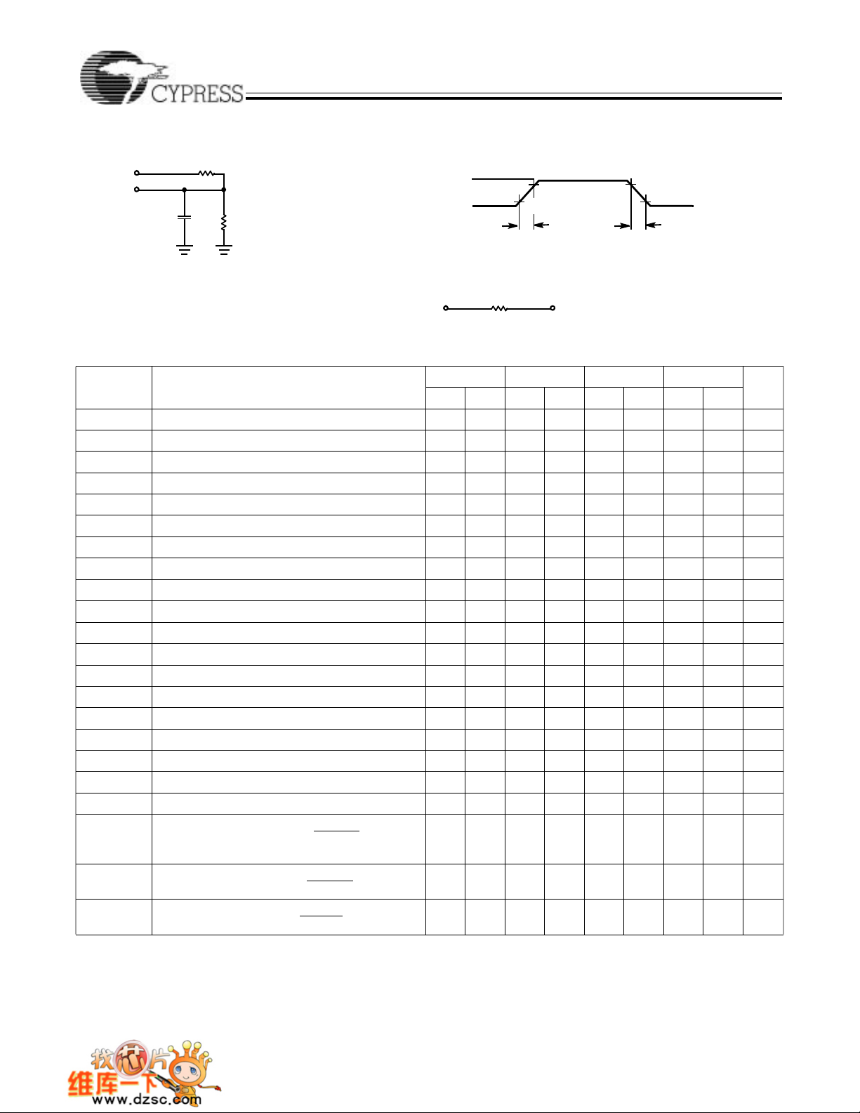
AC Test Loads and Waveforms
R1 1.1K
5V
OUTPUT
INCLUDING
C
JIG AND
SCOPE
L
Ω
R2
680Ω
4255–4
PRELIMINARY
[9, 10]
3.0V
GND
≤ 3ns ≤ 3
Equivalent to: THÉ VENIN EQUIVALENT
410Ω
OUTPUT 1.91V
ALL INPUT PULSES
90%
10%
Switching Characteristics Over the Operating Range
7C42X5–10 7C42X5–15 7C42X5–25 7C42X5–35
Parameter Description Min. Max. Min. Max. Min. Max. Min. Max. Unit
t
S
t
A
t
CLK
t
CLKH
t
CLKL
t
DS
t
DH
t
ENS
t
ENH
t
RS
t
RSR
t
RSF
t
PRT
t
RTR
t
OLZ
t
OE
t
OHZ
t
WFF
t
REF
t
PAFasynch
t
P AFsyn ch
t
P A Easyn ch
Notes:
9. C
L
10. CL = 5 pF for t
11. Pulse widths less than minimum values are not allowed.
12. Values guaranteed by design, not currently tested.
13. t
PAFasynch
Clock Cycle Frequency 100 66.7 40 28.6 MHz
Data Access Time 2 8 2 10 2 15 2 20 ns
Clock Cycle Time 10 15 25 35 ns
Clock HIGH Time 4.5 6 10 14 ns
Clock LOW Time 4.5 6 10 14 ns
Data Set-Up Time 3 4 6 7 ns
Data Hold Time 0.5 1 1 2 ns
Enable Set-Up Time 3 4 6 7 ns
Enable Hold Time 0.5 1 1 2 ns
Reset Pulse Width
[11]
10 15 25 35 ns
Reset Recovery Time 8 10 15 20 ns
Reset to Flag and Output Time 10 15 25 35 ns
Retransmit Pulse Width 30 35 45 55 ns
Retransmit Recovery Time 60 65 75 85 ns
Output Enable to Output in Low Z
[12]
0 0 0 0 ns
Output Enable to Output Valid 3 7 3 8 3 12 3 15 ns
Output Enable to Output in High Z
[12]
3 7 3 8 3 12 3 15 ns
Write Clock to Full Flag 8 10 15 20 ns
Read Clock to Empty Flag 8 10 15 20 ns
Clock to Programmable Almost-Full Flag
[13]
12 16 20 25 ns
(Asynchronous mode, VCC/SMODE tied to
V
)
CC
Clock to Programmable Almost-Full Flag
(Synchronous mode, V
/SMODE tied to VSS)
CC
Clock to Programmable Almost-Empty Flag
[13]
8 10 15 20 ns
12 16 20 25 ns
(Asynchronous mode, VCC/SMODE tied to VCC)
= 30 pF for all AC parameters except for t
, t
.
OHZ
, after program register write will not be valid until 5 ns + t
PAEa syn ch
OHZ
.
.
PAF (E)
5
CY7C4255
PRELIMINARY
CY7C4265
Switching Characteristics Over the Operating Range (continued)
7C42X5–10 7C42X5–15 7C42X5–25 7C42X5–35
Parameter Descriptio n Min. Max. Min. Max. Min. Max. Min. Max. Unit
t
PAEsynch
t
HF
t
XO
t
XI
t
XIS
t
SKEW1
t
SKEW2
t
SKEW3
Clock to Programmable Almost-Full Flag
(Synchronous mode, V
Clock to Half-Full Flag 12 16 20 25 ns
Clock to Expansion Out 6 10 15 20 ns
Expansion in Pulse Width 4.5 6.5 10 14 ns
Expansion in Set-Up Time 4 5 10 15 ns
Skew Time between Read Clock and Write
Clock for Full Flag
Skew Time between Read Clock and Write
Clock for Empty Flag
Skew Time between Read Clock and Write
Clock for Programmable Almost Empty and Programmable Almost Full Flags (Synchronous
Mode only)
/SMODE tied to VSS)
CC
10 15 18 20 ns
8 10 15 20 ns
5 6 10 12 ns
5 6 10 12 ns
6

CY7C4255
Switching Waveforms
Write Cycle Timing
WCLK
D
0–D17
WEN
FF
RCLK
REN
t
SKEW1
PRELIMINARY
t
t
CLKH
[14]
t
WFF
CLK
t
t
DS
CLKL
t
ENS
t
DH
t
ENH
t
WFF
CY7C4265
NO OPERATION
4255–6
Read Cycle Timing
RCLK
t
ENS
REN
EF
Q
0–Q17
t
OLZ
OE
WCLK
WEN
Notes:
14. t
15. t
is the mi nimum t ime bet ween a r ising RCLK edg e and a ris ing WC LK edge to guar antee tha t FF will go HIGH during the current clock cycle. If the time between the
SKEW1
rising edge of R CLK and the r ising edge of WCLK is less than t
is the minimum time between a rising WCLK edge and a rising RCLK edge to guarantee that EF will go HIGH during the current clock cycle. It the time between the
SKEW2
rising edge of WCLK and th e ris ing ed ge of RCLK is les s than t
t
t
CLKH
ENH
t
t
REF
A
t
CLK
t
OE
SKEW1
SKEW2
t
CLKL
NO OPERATION
t
REF
VALID DATA
[15]
t
SKEW2
, then FF may not c hange state un til the ne xt WCLK ri sing edge.
, then EF may not chan ge s tate unti l the next RC LK r ising edge.
t
OHZ
4255–7
7

CY7C4255
PRELIMINARY
Switching Waveforms (continued)
RS
LD
HF
[16]
t
RS
t
RSF
t
RSF
t
RSF
17
Reset Timing
,WEN,
REN
EF,PAE
FF,PAF,
Q0–Q
First Data Word Lat ency after Reset with Simultaneous Read and Write
t
RSR
CY7C4265
[17]
OE=1
=0
OE
4255–8
WCLK
t
DS
D0–D
WEN
17
t
ENS
D
(FIRSTVA LIDWRITE)
0
t
SKEW2
t
FRL
[18]
RCLK
EF
REN
Q
0–Q17
t
OLZ
OE
Notes:
16. The clocks (RCLK, WCLK) can be free-running during reset.
17. After reset, the outputs will be LOW if OE
18. When t
The Latency Timing applies only at the E mpty Boundary (EF = L OW).
19. The first word is available the cycle after EF goes H IGH, al ways.
> minimum specification, t
SKEW2
= 0 and three- state if OE = 1.
(maximum) = t
FRL
CLK
+ t
SKEW2
D
1
t
REF
. When t
t
OE
< minimum spe cification, t
SKEW2
D
2
t
A
(maximum) = either 2*t
FRL
D
3
[19]
t
A
D
0
+ t
CLK
SKEW2
or t
CLK
D
1
4255–9
+ t
SKEW2
D
4
.
8

CY7C4255
Switching Waveforms (continued)
Empty Flag Timing
WCLK
t
DS
D0–D
17
t
ENH
t
SKEW2
t
FRL
[18]
RCLK
Q
0–Q17
WEN
EF
REN
OE
t
ENS
PRELIMINARY
t
REF
CY7C4265
t
DS
D1D0
t
t
ENS
t
REF
t
A
ENH
t
SKEW2
t
FRL
[18]
D0
t
REF
4255–10
Full FlagTiming
WCLK
D0–D
17
FF
WEN
RCLK
REN
OE
Q
0–Q17
NO WRITE
[14]
t
SKEW1
t
WFF
t
t
ENS
ENH
LOW
t
A
DATA IN OUTPUT REGISTER
NO WRITE
t
DS
t
SKEW1
[14]
DATA WRITE
DATA WRITE
t
WFF
DATA READ
t
ENS
t
WFF
t
t
ENH
A
NEXT DATA READ
4255–11
9

CY7C4255
PRELIMINARY
Switching Waveforms (continued)
Half–Full Flag Timing
t
CLKH
WCLK
WEN
HF
RCLK
REN
Programmable Almost Empty Flag Timing
HALF FULLORLESS HALF FULLOR LESS
t
CLKH
t
ENS
t
ENH
t
CLKL
t
CLKL
CY7C4265
t
HF
t
ENS
HALF FULL + 1
OR MORE
t
HF
4255–12
WCLK
WEN
[20]
PAE
RCLK
REN
Notes:
is offset = n. Number of da ta wo rds into FIFO already = n.
20. PAE
t
ENS
t
ENH
t
PAE
t
ENS
N + 1 WORDS
IN FIFO
t
PAE
n WORDS IN FIFO
4255–13
10

CY7C4255
PRELIMINARY
Switching Waveforms (continued)
Programmable Almost Empty Flag Timing (applies only in SM O DE (SMODE is LOW))
ENS
ENS
[22]
t
ENH
t
ENH
t
CLKL
Note
21
t
PAE synch
t
ENS
N + 1 WORDS
INFIFO
t
ENS
WCLK
WEN
WEN2
PAE
RCLK
REN
t
CLKH
t
SKEW3
t
t
t
ENH
CY7C4265
Note
t
PAE synch
23
4255–14
Programmable Almost Full FlagTiming
t
CLKH
Note
WCLK
WEN
[25]
PAF
RCLK
REN
Notes:
21. PAE offset − n.
22. t
23. If a read is preformed on this rising edge of the read clock, there will be Empty + (n−1) words in the FIFO when PAE goes LOW.
24. PAF offset = m. Number of data words written into FIFO already = 8192 − (m + 1) for the CY7C4255 and 16384 − (m + 1) for the CY7C4265.
25. PAF is offset = m.
26. 8192 − m words in CY7C4255 and 16384 - m words in CY7C4265.
27. 8192 − (m + 1) words in CY7C4255 and 16384 - (m + 1) CY7C4265.
is the minimum time between a risi ng WCLK and a rising RCLK edge for P AE to change stat e during that clock cycle. If the time between the edg e of WCLK and the
SKEW3
rising RCLK is less t han t
, then PAE may not change s tate unti l the next R CLK.
SKEW3
24
t
ENS
t
ENH
t
CLKL
t
PAF
FULL– M WORDS
INFIFO
t
ENS
[26]
t
FULL– (M+1) WORDS
IN FIFO
PAF
[27]
4255–15
11

CY7C4255
PRELIMINARY
Switching Waveforms (continued)
Programmable Al most Full Flag Timing (applies only in SM O DE (SMODE is LOW))
Note
28
Note
29
t
PAF
FULL– M WORDS
t
SKEW3
t
ENS
IN FIFO
[30]
t
ENS
WCLK
WEN
WEN2
PAF
RCLK
REN
t
CLKH
t
CLKL
t
t
ENH
ENS
t
t
ENH
ENS
FULL– M + 1 WORDS
IN FIFO
[26]
t
ENH
CY7C4265
t
PAF synch
4255–16
Write Programmable Registers
t
CLK
t
CLKH
WCLK
t
ENS
LD
t
ENS
WEN
t
DS
D
0–D17
PAE OFFSET
Notes:
28. If a write is performed on this rising edge of the write clock, there will be Full − (m − 1) words of the FIFO when PAF
29. PAF offset = m.
30. t
is the minimum time between a rising RCLK and a rising WCLK edge for P AF to c han ge sta te d uring that cloc k c ycle. If th e t ime bet ween the edge of RC LK and the
SKEW3
rising edge of W CLK is less tha n t
, then PAF may not change state unt il the next WCLK r ising edge.
SKEW3
t
CLKL
t
ENH
t
DH
PAF OFFSET
PAE OFFSET
D0–
D
11
goes LOW.
4255–17
12

CY7C4255
Switching Waveforms (continued)
Read Programmable Register s
t
CLK
t
CLKH
RCLK
t
ENS
LD
t
ENS
WEN
Q
0–Q17
Write ExpansionOut Timing
t
CLKH
WCLK
WXO
t
ENS
WEN
PRELIMINARY
t
CLKL
t
ENH
t
A
UNKNOWN
Note 31
t
XO
Note 31
t
XO
PAE OFFSET
CY7C4265
PAF OFFSET PAE OFFS ET
4255–18
4255–19
Read Expansion Out Timing
WCLK
RXO
REN
Write E xpansion In Tim ing
WXI
WCLK
Notes:
31. Write to Last Physical Location.
32. Read from Last Physical Location.
t
ENS
t
CLKH
t
t
XIS
XI
Note 32
t
XO
t
XO
4255–20
4255–21
13

CY7C4255
PRELIMINARY
Switching Waveforms (continued)
Read Expansion I n Timin g
t
XI
RXI
t
RCLK
Retransmit Timing
FL/RT
REN/WEN
EF/FF
and all
async flags
HF/PAE/PAF
Notes:
33. Clocks are free running in this case.
34. The flags may change state during Retransmit as a result of the offset of the read and write pointers, but flags will be valid at t
35. For the synchronous PAE and PAF flags (S MODE), an appr opri ate cloc k cycl e is nec essar y after t
[33, 34, 35]
t
PRT
RTR
XIS
to update these f lags.
t
RTR
CY7C4265
.
RTR
4255–22
4255–23
14

CY7C4255
PRELIMINARY
Architecture
The CY7C4256/65 consists of an array of 8K/16K words of 18
bits each (implemented by a dual-port array of SRAM cells), a
read pointer, a write pointer, control sig nals (RCLK, WCLK,
REN
, WEN, RS), and flags (EF, PAE, HF, PAF, FF). The
CY7C4255/65 also incl udes the control signals WXI
RXO
for depth expansion.
Resetting the FIFO
Upon power-up, the FIFO must be reset with a Reset (RS)
cycle. This causes the FIFO to enter the Empty condition signified by
EF
being LOW. All data outputs go LOW after the falling edge of RS
only if OE is asserted. In order for the FIFO to reset to its default state,
a falling edge must occur on RS
while RS
is LOW.
and the user must not read or write
FIFO Operation
When the WEN signal is active (LOW), data present on the D
pins is written into the FIFO on each rising edge of the WCLK signal.
Similarly, when the REN
ory will be presented on the Q
sented on each rising edge of RCLK while REN
OE
is LOW. REN must set up t
read function. WEN
write function.
An output enable (OE
outputs when OE is deasserted. When OE is enabled (LOW), data
in the output register will be available to the Q
If devices are cascaded, the OE
FIFO that is read enabled.
The FIFO contains overflow circuitry to disallow additional
writes when the FIFO is full, and under flow circuitry to disallow
additional reads when the FIFO is empty. An empty FIFO
maintains the data of the last valid read on its Q
even after additional reads occur.
signal is active LOW, data in the FIFO mem-
must occur tENS before WCLK for it to be a valid
) pin is provided to three-state the Q
outputs. New data wil l be pre-
0 – 17
before RCLK for it to be a valid
ENS
function will only output data on the
0 – 17
Programm ing
The CY7C4255/65 devices contain two 14-bit offset registers.
Data present on D
distance from Empty (Full) that the Almost Empty (Almost Full) flags
become active. If the user elects not to program the FIFO’s flags, the
default offset values are used (see
is set LOW and WEN
into the Empty offset register on the first LOW-to-HIGH transition of
the write clock (WCLK). When the LD
then data is written into the Full offset register on the second
LOW-to-HIGH transition of the write clock (WCLK). The third transition of the write clock (WCLK) again writes to the Empty offset register
(see
Ta b l e 1
one time. One or two offset registers can be written and then, by bringing the LD
). Writing all offset registers does not have to occur at
pin HIGH, the FIFO is returned to normal read/write oper-
during a program write will determine the
0–13
Table 2
). When the Load LD pin
is set LOW, data on the inputs D
pin and WEN are held LOW
, RXI, WXO,
0–17
is active LOW and
0 – 17
outputs after tOE.
outputs
0 – 17
is written
0 – 13
CY7C4265
ation. When the LD
register in sequence is written.
The contents of the offset registers can be read on the output
lines when the LD
can be read on the LOW-to-HIGH transition of the read clock (RCLK).
Table 1. Write Offset Register.
LD WEN WCLK
0 0 Writing to offset registers:
0 1 No Operation
1 0 Write Into FIFO
1 1 No Operation
Flag Operation
The CY7C4255/65 devices provide five flag pins to indicate
the condition of th e FIFO contents. Empty and Full are synchronous. PAE
V
.
SS
Full Flag
The Full Flag (F F
are inhibited whenever FF
FF
is synchronized to WCLK, i.e., it is exclusively updated by ea ch
rising edge of WCLK.
Empty Flag
The Empty Flag (EF
operations are inhibited whenever EF
of REN
. EF is synchronized to RCLK, i.e., it is exclusively updated by
each rising edge of RCLK.
Programmable Almost Empty/Al most Ful l Flag
The CY7C4255/65 features programmable Almost Empty and
Almost Full Flags. Each flag can be programmed (described
in the Programming section) a specific distance from the corresponding boundary flags (Empty or Full). When the FIFO
contains the number of words or fewer for which the flags h ave
been programmed, the P A F
the FIFO is either Almost Full or Almost Empt y. See
description of programmable flags.
When the SMODE
caused by the rising edge of the write clock and the P AE
is caused by the rising edge of the read clock.
pin is set LOW, and WEN is LOW, the next of fset
pin is set LOW and REN is set LOW; then, data
[36]
Empty Offset
Full Offset
and PAF are synchronous if VCC/SMODE is tied to
) will go LOW when device is Full. Write operations
is LOW regardless of the state of WEN.
) will go LOW when the device is empty . Read
or P AE will be asserted, signifying that
pin is tied LOW, the P AF flag signal transition is
Selection
is LOW, regardless of the state
Table 2
for a
flag transition
15

CY7C4255
CY7C4265
Retransmit
PRELIMINARY
nal read pointer to the first physical location of the FIFO. WCLK and
RCLK may be free running but m ust be di sabled dur ing and t
The retransmit feature is beneficial when transferring packets
of data. It enables the receipt of data to be acknowledged by
the receiver and retransmitted if necessary.
The Retransmit (RT) input is active in the stand-alone and
width expansion modes. The retransmit feature is i ntended for
use when a number of writes equal to or less than the depth
of the FIFO have occurred and at least one word has been
read since the last RS
cycle. A HIGH pulse on RT resets the inter -
after the retransmit pulse. With every valid read cycle after retransmit,
previously accessed data is read and the read pointer is incriminated
until it is equal to the write pointer . Flags are governed by the relative
locations of the read and write pointers and are updated during a
retransmit cycle. Data written to the FIFO af ter activation of RT are
transmitted also.
The full depth of the FIFO can be repeatedly retransmitted.
Table 2. Flag Truth Table.
Number of Words in FIFO
FF PAF HF PAE EF7C4255 – 8K x 18 7C4265 – 16K x 18
0 0 H H H L L
1 to n
[37]
1 to n
[37]
H H H L H
(n+1) to 4096 (n+1) to 8192 H H H H H
4097 to (8192–(m+1)) 8193 to (16384 –(m+1)) H H L H H
(8192–m)
[38]
to 8191 (16384–m)
[38]
to 16383 H L L H H
8192 16384 L L L H H
Notes:
36. The same selection sequence applies to reading from the registers. REN
37. n = Empty Offset (Default Values: CY7C4255/CY7C4265 n = 127).
38. m = Full Offset (Default Values: CY7C4255/CY7C4265 n = 127).
is enabled and read i s perfor med o n the LOW-t o-HIGH tr ansiti on of RCLK.
RTR
16

CY7C4255
PRELIMINARY
Width Expansion Configuration
The CY7C4255/65 can be expanded in width to provide word
widths greater than 18 in increments of 18. During width expansion mode all control line inputs are comm on and all flags
are available. Empty (Full) flags should be created by ANDing
7C4255
7C4265
(RS)
18
DATA IN (D)
WRITE CLOCK(WCLK)
WRITE ENABLE(WEN
LOAD(LD
PROGRAMMABLE(PAE
HALF FULL FLAG (HF
FULL FLAG (FF
)
RESET
1836
)
)
)
)
FF EF
CY7C4265
the Empty (Full) flags of every FIFO; the PAE
can be detected from any one device. This technique will avoid
reading d ata from, or writi ng data to the FI FO that is “staggered” by one clock cycle due to the variations in skew between RCLK and WCLK.
by using two CY7C4255/65s.
RESET ( RS)
18
7C4255
7C4265
FF
Figure 1
READ CLOCK (RCLK)
READ ENABLE (REN
OUTPUT ENABLE (OE
PROGRAMMABLE (PAF
EF
demonstrates a 36-word width
EMPTY FLAG
DATA OUT(Q)
18 36
and PAF flags
)
)
)
(EF)
FIRST LOAD(FL)
WRITE EXPANSION IN (WXI
READ EXPANSION IN (RXI
Figure 1. Block Diagram of 8K x18/16K x 18Synchronous FIFO Memory Used in a Width Expansion Configuration.
)
)
4255–24
17

CY7C4255
PRELIMINARY
Depth Expansion Configuration
(with Program mab le Flags )
The CY7C4255/65 can easily be adapted to applications requiring more than 8192/16384 words of buffering.
shows Depth Expansion using three CY7C42X5s. Maximum depth
is limited only by signal loading. Follow these steps:
1. The first device must be desig nated by grounding the First
Load (FL
2. All other devices must have FL
) control input.
in t h e HIGH s ta t e.
Figure 2
V
CC
FL
FF EF
PAF
WXO RXO
7C4255
7C4265
WXI RXI
CY7C4265
3. The Write Expansion Out (WXO
tied to the Write Expansion In (WXI
4. The Read Expansion Out (RXO
tied to the Read Expansion In (RXI
5. All Load (LD
6. The Half-Full Flag (HF
Configuration.
, FF, PAE, and PAF are created with composite flags by
7. EF
ORing together these respective flags for monitoring. The
composite PAE
PAE
) pins are tied together.
) is not available in the Depth Expansion
and PAF flags are not precise.
) pin of each device must be
) pin of the next device.
) pin of each device must be
) pin of the next device.
WXO RXO
DATAI N (D) DATA OUT(Q)
V
CC
WRITECLOCK(WCLK)
LOAD
(LD)
WRITEENABLE
RESET
FF
PAF
(RS)
FIRST LOAD(FL)
(WEN)
7C4255
7C4265
FL
FF EF
PAF
WXI RXI
WXO
7C4255
7C4265
FF EF
PAF
WXI RXI
PAE
RXO
PAE
READCLOCK
READENABLE
OUTPUTENABLE
(RCLK)
(REN)
(OE)
EF
PAE
4255–25
Figure 2. Block Diagram of 8Kx18/16Kx18 Synchronous FIFO Memory
with Programmable Flags used in Depth Expansion Configuration.
18

CY7C4255
PRELIMINARY
Ordering Info rma tio n
8Kx18 Deep Sync FIFO
Speed
(ns) Ordering Code
10 CY7C4255–10AC A65 64-Lead Thin Quad Flatpack Commercial
CY7C4255–10JC J81 68-Lead Plastic Leaded Chip Carrier
CY7C4255–1 0AI A65 64-Lead Thin Quad Flatpack Industrial
CY7C4255–10JI J81 68-Lead Plastic Leaded Chip Carrier
15 CY7C4 255–1 5AC A65 64-Lead Thin Quad Flatpack Commercial
CY7C4255–15JC J81 68-Lead Plastic Leaded Chip Carrier
CY7C4255–1 5AI A65 64-Lead Thin Quad Flatpack Industrial
CY7C4255–15JI J81 68-Lead Plastic Leaded Chip Carrier
25 CY7C4 255–2 5AC A65 64-Lead Thin Quad Flatpack Commercial
CY7C4255–25JC J81 68-Lead Plastic Leaded Chip Carrier
CY7C4255–2 5AI A65 64-Lead Thin Quad Flatpack Industrial
CY7C4255–25JI J81 68-Lead Plastic Leaded Chip Carrier
35 CY7C4 255–3 5AC A65 64-Lead Thin Quad Flatpack Commercial
CY7C4255–35JC J81 68-Lead Plastic Leaded Chip Carrier
CY7C4255–3 5AI A65 64-Lead Thin Quad Flatpack Industrial
CY7C4255–35JI J81 68-Lead Plastic Leaded Chip Carrier
Package
Name
Package
Type
Operating
CY7C4265
Range
16Kx18 Deep Sync FIFO
Speed
(ns)
10 CY7C4265–10AC A65 64-Lead Thin Quad Flatpack Commercial
15 CY7C4 265–1 5AC A65 64-Lead Thin Quad Flatpack Commercial
25 CY7C4 265–2 5AC A65 64-Lead Thin Quad Flatpack Commercial
35 CY7C4 265–3 5AC A65 64-Lead Thin Quad Flatpack Commercial
Document #: 38-00468-A
Ordering Code
CY7C4265–10JC J81 68-Lead Plastic Leaded Chip Carrier
CY7C4265–1 0AI A65 64-Lead Thin Quad Flatpack Industrial
CY7C4265–10JI J81 68-Lead Plastic Leaded Chip Carrier
CY7C4265–15JC J81 68-Lead Plastic Leaded Chip Carrier
CY7C4265–1 5AI A65 64-Lead Thin Quad Flatpack Industrial
CY7C4265–15JI J81 68-Lead Plastic Leaded Chip Carrier
CY7C4265–25JC J81 68-Lead Plastic Leaded Chip Carrier
CY7C4265–2 5AI A65 64-Lead Thin Quad Flatpack Industrial
CY7C4265–25JI J81 68-Lead Plastic Leaded Chip Carrier
CY7C4265–35JC J81 68-Lead Plastic Leaded Chip Carrier
CY7C4265–3 5AI A65 64-Lead Thin Quad Flatpack Industrial
CY7C4265–35JI J81 68-Lead Plastic Leaded Chip Carrier
Package
Name
Package
Type
Operati ng
Range
19

CY7C4255
Package Diagrams
PRELIMINARY
64-Lead Thin Plastic Quad Flat Pack A65
CY7C4265
68-Lead Plastic LeadedC hip Carrier
© Cypress Semiconductor Corporation, 1996. The information contained herein is subject to change without notice. Cypress Semiconductor Corporation assumes no responsibility for the use
of any circ uitry other than circui try embodi ed in a Cypress Semi conductor p roduct. Nor does it convey or imply any li cense under patent or other rights . Cypress Semi conductor does not authori ze
its products for use as critical components in life-support systems where a malfunction or failure may reasonably be expected to result in significant injury to the user. The inclusion of Cypress
Semiconductor products in life-support systems application implies that the manufacturer assumes all risk of such use and in doing so indemnifies Cypress Semiconductor against all charges.
J81
 Loading...