

64 x 4 Cascadable FIFO
64 x 5 Cascadable FIFO
CY7C401/CY7C403
CY7C402/CY7C404
1CY7C40 2
查询CY7C401-15LMB供应商
Features
• 64 x 4 (CY7C401 and CY7C403)
64 x 5 (CY7C402 and CY7C404)
High-speed first-in fi rst-out memory (FI FO)
• Processed with high-speed CMOS for optimum
speed/power
• 25-MHz data rates
• 50-ns bubble-through time—25 MHz
• Expandable in word width and/or length
• 5-volt power supply ± 10% tolerance, both commercial
and milita ry
• Independent asynchronous inputs and outputs
• TTL-compatible interface
• Output enable function available on CY7C403 and
CY7C404
• Capable of withstanding greater than 2001V electrostatic discharge
• Pin compatible with MMI 67401A/67402A
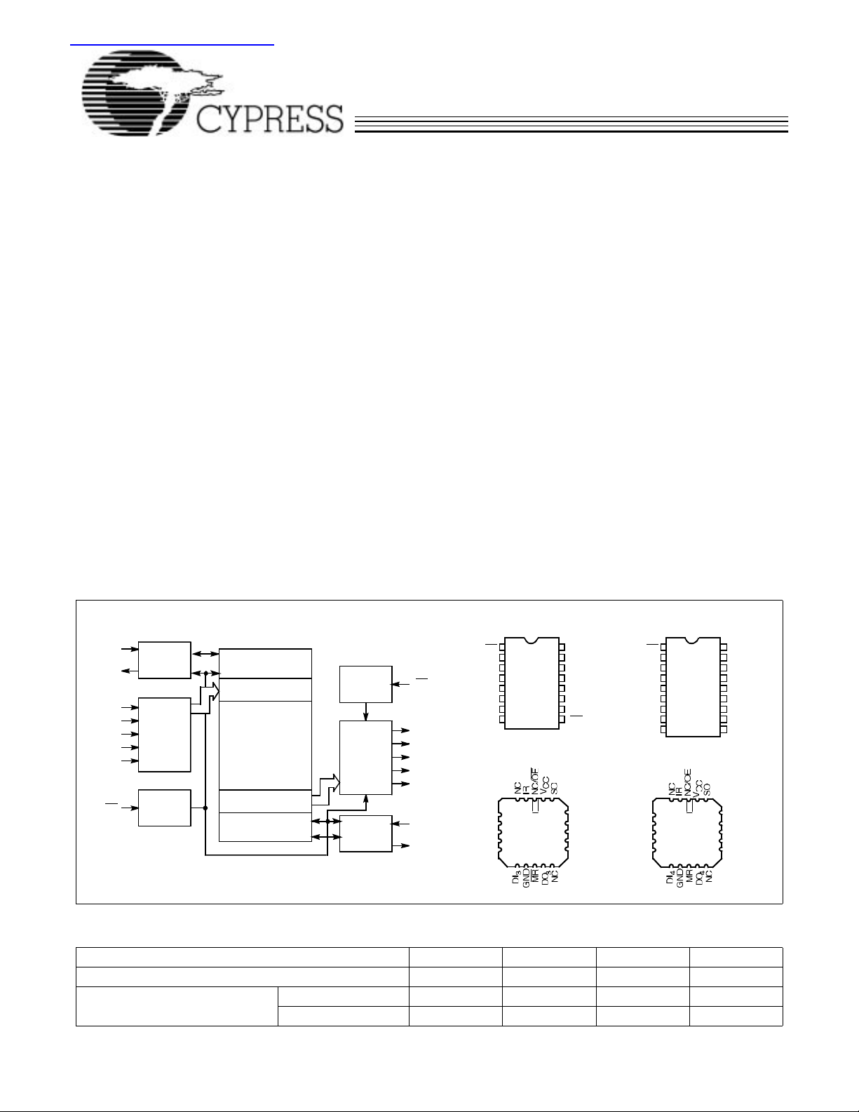
Functional Description
The CY7C401 and CY7C403 are asynchronous first-in
first-out (FIFOs) organized as 64 four-bit words. The CY7C402
and CY7C404 are similar FIFOs organized as 64 five-bit
words. Both the CY7C403 and CY7C404 have an output enable (OE) function.
The devices accept 4- or 5-bit words at the data input (DI
DI
) under the control of the shift in (SI) input. The stored
n
words stack up at the output (DO
were entered. A read command on the shift out (SO) input
– DOn) in the order they
0
–
0
causes the next to last word to move to the output and all data
shifts down once in the stack. The input ready (IR) signal acts
as a flag to indicate when the input is ready to accept new data
(HIGH), to indicate when the FIFO is full (LOW), and to provide
a signal for a cascading. The output ready (OR) signal is a flag
to indicate the output contains valid data (HIGH), to indicate
the FIFO is empty (LOW), and to provide a signal for cascading.
Parallel expansion for wider words is accomplished by lo gically ANDing the IR and OR signals to form c omposite signals.
Serial e xpansion is accomplished by tying the data inputs of
one device to the data outputs of the previous device. The IR
pin of the receiving device is connected to the SO pi n of the
sending device, and the OR pin of the sending device is connected to the SI pin of the receiving device.
Reading and writing operations are completely asynchronous,
allowing the FIFO to be used as a buffer between two digital
machines of widely differing operating frequencies. The
25-MHz operation makes these FIFOs ideal for high-speed
communication and controller applications.
Logic Block Diagram Pin Configurations
DI
DI
DI
DI
(DI4)
MR
DI
DI
DI
DI
NC
IR
SI
0
1
2
3
SI
0
1
2
DIP
1
2
3
CY7C401
4
CY7C403
5
6
7
8
LCC
321 19
4
5
CY7C401
6
CY7C403
7
8
910111213
16
15
14
13
12
11
10
C401–2
20
V
SO
OR
DO
DO
DO
DO
9
MR
18
17
16
15
14
C401–3
NC
OR
DO
DO
DO
CC
0
1
2
3
0
1
2
(CY7C402) NC
(CY7C404) OE
DI
DI
DI
DI
C401–1
(CY7C401) NC
(CY7C403) OE
OE
DO
0
DO
1
DO
2
DO
3
(DO4)
SO
OR
GND
DI
DI
DI
SI
IR
INPUT
CONTROL
LOGIC
0
1
DATAIN
2
3
MASTER
RESET
WRITEPOINTER
WRITE MULTIPLEXER
MEMORY
ARRAY
READ MULTIPLEXER
READ POINTER
OUTPUT
ENABLE
DATAIN
OUTPUT
CONTROL
LOGIC
IR
SI
DI
DI
DI
DI
DI
SI
0
1
2
3
1
2
3
4
0
5
1
6
2
7
3
8
4
9
321 19
4
5
CY7C402
6
CY7C404
7
8
910111213
DIP
CY7C402
CY7C404
LCC
20
18
17
16
15
14
13
12
11
10
C401–4
18
17
16
15
14
C401–5
Selectio n Guide
7C401/2–5 7C40X–10 7C40X–15 7C40X–25
Operating Frequency (MHz) 5 10 15 25
Maximum Operating
Current (mA)
Commercial 75 75 75 75
Military 90 90 90
OR
DO
DO
DO
DO
V
SO
OR
DO
DO
DO
DO
DO
MRGND
CC
0
1
2
3
4
0
1
2
3
Cypress Semiconductor Corporation • 3901North First Street • San Jose • CA 95134 • 408-943- 2600
March 1986 – Revised April 1995
CY7C401/CY7C403
Maximum Ratings
(Above which the useful life may be impaired. For user guidelines, not tested.)
Storage Temperature .................................–65°C to +150°C
Ambient Temperature with
Output Current, into Outputs (LOW)..................... ....... 20 mA
Static Discharge Voltage ...........................................>2001V
(per MIL-STD-883, Method 3015)
Latch-Up Current .....................................................>200 mA
Operating Range
CY7C402/CY7C404
Power Applied.............................................–55°C to +125°C
Supply Voltage to Ground Potential............... –0.5V to +7.0V
DC Voltage Applied to Outputs
in High Z State ............................................... –0.5V to +7.0V
DC Input Voltage............................................–3.0V to +7.0V
Range
Commercial 0°C to +70°C 5V ±10%
[1]
Military
Ambient
Temperature V
–55°C to +125°C 5V ±10%
Power Dissipation............................... ...........................1.0W
Electrical Characteristics Over the Operating Range (Unless Otherwise Noted)
[2]
7C40X–10, 15, 25
Parameter Descrip tion Test Conditions Min. Max. Unit
V
V
V
V
I
V
I
I
I
IX
OZ
OS
CC
OH
OL
IH
IL
CD
[3]
Output HIGH Voltage VCC = Min., IOH = –4.0 mA 2.4 V
Output LOW Voltage VCC = Min., IOL = 8.0 mA 0.4 V
Input HIGH Voltage 2.0 6.0 V
Input LOW Voltage –3.0 0.8 V
Input Leakage Current GND ≤ VI ≤ V
Input Diode Clamp Voltage
Output Leakage Current GND ≤ V
Output Short Circuit Current
[3]
OUT
[4]
Output Disabled (CY7C403 and CY7C404)
VCC = Max., V
Power Supply Current VCC = Max., I
CC
≤ VCC, VCC = 5.5V
= GND –90 mA
OUT
= 0 mA Commercial 75 mA
OUT
–10 +10 µA
–50 +50 µA
Military 90 mA
CC
Capacitance
[5]
Parameter Description Test Conditions Max. Unit
C
IN
C
OUT
Notes:
1. T
is the “instant on” case temperature.
A
2. See the last page of this specification for Group A subgroup testing information.
3. The CMOS process does not provide a clamp diode. However, the FIFO is insensitive to –3V dc input levels and –5V undershoot pulses of less than 10 ns
(measured at 50% output).
4. For test purposes, not more than one output at a time should be shorted. Short circuit test duration should not exceed 30 seconds.
5. Tested initially and after any design or process changes that may affect these parameters.
Input Capacitance TA = 25°C, f = 1 MHz,
V
= 4.5V
Output Capacitance 7 pF
CC
5 pF
2
CY7C401/CY7C403
CY7C402/CY7C404
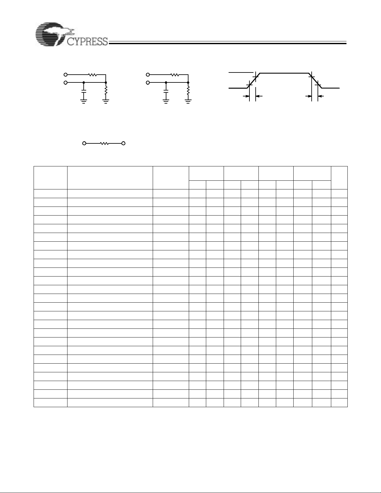
AC Test Loads and Waveforms
ALL INPUT PULSES
and 30-pF load
OL/IOH
90%
90%
10%
is tested with 5-pF load capacitance as
HZOE
10%
[7]
30 pF
R1 437Ω
R2
272Ω
5V
OUTPUT
INCLUDING
JIG AND
SCOPE
5V
OUTPUT
INCLUDING
JIG AND
SCOPE
(a) (b)
Equivalent to: THÉ VENIN EQUIVALENT
OUTPUT 1.73V
167Ω
C401–8
Switching Characteristics Over the Operating Range
5 pF
R1 437Ω
3.0V
R2
272Ω
C401–6 C401–7
[2, 6]
GND
≤ 5ns ≤ 5ns
7C401–5
Test
Parameter Description Min. Max. Min. Max. Min. Max. Min. Max. Unit
f
O
t
PHSI
t
PLSI
t
SSI
t
HSI
t
DLIR
t
DHIR
t
PHSO
t
PLSO
t
DLOR
t
DHOR
t
SOR
t
HSO
t
BT
t
SIR
t
HIR
t
PIR
t
POR
t
PMR
t
DSI
t
DOR
t
DIR
t
LZMR
t
OOE
t
HZOE
Notes:
6. Test condition s assu me signa l tra nsit ion tim e of 5 ns or less, timin g refere nce levels o f 1.5V and output loading of the spe cifi ed I
capacitance, as in part (a) of AC Test Loads and Waveforms.
7. Commercial/Military
8. I/fO > t
9. t
SSI
10. t
SIR
11. All data outputs will be at LOW level after reset goes HIGH until data is entered into the FIFO.
12. HIGH-Z transitions are referenced to the steady-state VOH –500 mV and VOL +500 mV levels on the output. t
in part (b) of AC Test Loads and Waveforms.
Operating Frequency Note 8 5 10 15 25 MHz
SI HIGH Time 20 20 20 11 ns
SO LOW Time 45 30 25 20 ns
Data Set-Up to SI Note 9 0 0 0 0 ns
Data Hold from SI Note 9 60 40 30 20 ns
Delay, SI HIGH to IR LOW 75 40 35 21/22 ns
Delay, SI LOW to IR HIGH 75 45 40 28/30 ns
SO HIGH Time 20 20 20 11 ns
SO LOW Time 45 25 25 20 ns
Delay, SO HIGH to OR LOW 75 40 35 19/21 ns
Delay, SO LOW to OR HIGH 80 55 40 34/37 ns
Data Set-Up to OR HIGH 0 0 0 0 ns
Data Hold from SO LOW 5 5 5 5 ns
Bubble-Through Time 200 10 95 10 65 10 50/60 ns
Data Set-Up to IR Note 10 5 5 5 5 ns
Data Hold from IR Note 10 30 30 30 20 ns
Input Ready Pulse HIGH 20 20 20 15 ns
Output Ready Pulse HIGH 20 20 20 15 ns
MR Pulse Width 40 30 25 25 ns
MR HIGH to SI HIGH 40 35 25 10 ns
MR LOW to OR LOW 85 40 35 35 ns
MR LOW to IR HIGH 85 40 35 35 ns
MR LOW to Output LOW Note 11 50 40 35 25 ns
Output Valid from OE LOW — 35 30 20 ns
Output High Z from OE HIGH Note 12 — 30 25 15 ns
+ t
PHSI
and t
and t
, I/fO > t
DHIR
apply when memory is not full.
HSI
apply when memory is full, SI is high and minimum b ubble-t hr ough (tBT) conditions exist.
HIR
PHSO
+ t
DHOR
Conditions
7C402–5
7C40X–10 7 C40X–15 7C40X–25
3

CY7C401/CY7C403
Operational Description
Concept
Unlike traditional FIFOs, these devices are designed using a
dual-port memory, read and write pointer, and control logic.
The read and write pointers are incremented by the SO and SI
respectively. The availability of an empty space to shift in data
is indicated by the IR signal, while the presence of data at the
output is indicated by the OR signal. The conventional concept
of bubble-through is absent. Instead, the delay for input data
to appear at the output is the time required to move a pointer
and propagate an OR signal. The output enable (OE
provides the capability to OR tie multiple FIFOs together on
a common bus.
Resetting the FIFO
Upon power-up, the FIFO must be reset with a master reset
(MR) signal. This causes the FIFO to enter an empty condition
signified by the OR signal being LOW at the same time the IR
signal is HIGH. In this condition, the data outputs (DO
will be in a LOW state.
Shifting Data In
Data is shifted in on the rising edge of the SI signal. This loads
input data into the first word location of the FIFO. On the falling
edge of the SI signal, the write pointer is moved to the next
word position and the IR signal goes HIGH, indicating the
readiness to accept new data. If the FIFO is full, the IR will
remain LOW until a word of data is shifted out.
Shifting Data Out
Data is shifted out of the FIFO on the falling edge of the SO
signal. This causes the internal read pointer to be advanced to
the next word location. If data is present, valid d ata will a ppear
on the outputs and the OR signal will go HIGH. If data is not
present, the OR signal will stay LOW indicating the FIFO is
empty. Upon the rising edge of SO, the OR signal goes LOW.
The data outputs of the FIFO should be sampled with
edge-sensitive type D flip-f lops (or equivalent), using the SO
signal as the clock input to the flip-flop.
Bubble-Through
Two bubble-through conditions exist. The first is when the device is empty. After a word is shifted into an empty device, the
data propagates to the output. After a delay, the OR flag goes
HIGH, indicating valid data at the output.
The second bubble-through condition occurs when the device
is full. Shifting data out creates an empty location th at propagates to the input. After a delay, the IR flag goes HIGH. If the
SI signal is HIGH at this time, data on the input will be shifted
in.
Possible Minimum Pulse Width Violation at the Boundary
Conditions
If the handshaking signals IR and OR are not properly used to
generate the SI and SO signals, it is possible to violate the
minimum (effective) SI and SO positive pulse widths at the full
and empty boundaries.
When this violation occurs, the operation of the FIFO is unpredictable. It must then be reset, and all data is lost.
) signal
– DOn)
0
CY7C402/CY7C404
Application of the 7C403–25/7C404–25 at 25 MHz
Application of the CY7C403 or CY7C404 Cypress CMOS
FIFOs requires knowledge of characteristics that are not easily
specified in a datasheet, but which are necessary for reliable
operation under all conditions, so we will specify them here.
When an empty FIFO is filled with init ial information at maximum “shift in” SI f requency, followed by immediate shifting out
of the data also at maximum “shift out” SO frequency, the designer must be aware of a window of time which follows the
initial rising edge of the OR signal, d uring which time the SO
signal is not recognized. This condition exists only at
high-speed operation where more than one SO may be generated inside the prohibited window. This condition does not
inhibit the operation of the FIFO at full-frequency operation,
but rather delays the full 25-MHz operation until after the window has passed.
There are several implementation techniques for managing
the window so that all SO signals are recognized:
1. The first involves delaying SO operation such that it does
not occur in the critical window. This can be accomplished
by causing a fixed delay of 40 ns “initiated by the SI signal
only when the FIFO is empty” to inhibit or gate the SO activity. However, this requires that the SO operation be at
least temporarily synchronized with the input SI operation.
In synchronous applications this may well be possible and
a valid solution.
2. Another solution not uncommon in synchronous applications is to only begin sh ifting data out of th e FIFO when it is
more than half full. This is a common method of FIFO application, as earlier FIFOs could not be operated at maximum frequency wh en near full or empty. Although Cypress
FIFOs do not have this limitation, any system designed in
this manner will not encounter the window condition described above.
3. The window may also be managed b y not allowing the fi rst
SO sign al t o occu r until the window in question has passed.
This can be accomplished by delaying the SO 40 ns from
the rising edge of the initial OR signal. This however involves the requirement that this only occurs on the first occurrence of data being loaded into the FIFO from an empty
condition and therefore requires the knowledge of IR and
SI conditions as well as SO.
4. Handshaking with the OR signal is a third method of avoiding the window in question. With this technique the rising
edge of SO, or the fact that SO signal is HIGH, will cause
the OR signal to go LOW. The SO signal is not taken LOW
again, advancing the internal pointer to the next data, until
the OR signal goes LOW. This ensures that the SO pulse
that is initiated in the window will be automatically extended
long enough to be recognized.
5. There remains the decision as to what signal will be used
to latch the data from the output of the FIFO into the receiving source. The leading edge of the SO signal is most appropriate because data is guaranteed to be stable prior to
and after the SO leading edge for each FIFO. This is a
solution for any number of FIFOs in parallel.
Any of the above solutions will ensure the correct operation of
a Cypress FIFO at 25 MHz. The specific implemen tation is left
to the designer and is dependent on the specific application
needs.
4

CY7C401/CY7C403
Switching Waveforms
Data In Timing Diagram
SHIFT IN
INPUT READY
DATA IN
Data Out Timing Diagram
OUT
SHIFT
t
t
SSI
PHSI
t
HSI
I/f
O
t
PLSI
t
DLIR
I/f
O
I/f
O
t
DHIR
I/f
O
CY7C402/CY7C404
C401–9
t
PHSO
OUTPUT READY
t
HSO
DATA OUT
BubbleThrough, Data Out To Data In
SHIFT
OUT
SHIFT IN
INPUT READY
Diagram
t
PLSO
t
DHOR
t
DLOR
t
BT
t
PIR
t
SOR
C401–10
DATA IN
t
SIR
t
HIR
C401–11
5

CY7C401/CY7C403
Switching Waveforms (continued)
Bubble Through, Data In T o Data Out Diagram
SHIFT
IN
SHIFT OUT
OUTPUT READY
DATA OUT
Master Reset Timing Diagram
t
PMR
CY7C402/CY7C404
t
BT
t
SOR
t
POR
C401–12
MASTER RESET
INPUT READY
OUTPUT READY
SHIFT IN
DATA OUT
Output Enable Timing Diagram
OUTPUT ENABLE
DATA OUT
t
HZOE
t
LZMR
t
DIR
t
DOR
NOTE 10
t
DSI
t
OOE
C401–13
C401–14
6

CY7C401/CY7C403
T y pical DC and AC Characteristics
NORMALIZED SUPPLY CURRENT
vs. SUPPLY VOLTAGE
1.2
1.0
0.8
0.6
0.4
4.0 4.5 5.0 5.5 6.0
SUPPLY VOLTAGE (V)
NORMALIZED FREQUENCY
vs. SUPPLY
1.3
1.2
1.1
1.0
0.9
0.8
4.0 4.5 5.0 5.5 6.0
SUPPLY VOLTAGE (V)
V
=5.0V
IN
T
=25°C
A
VOLTAGE
NORMALIZED SUPPLY CURRENT
vs. AMBIENT TEMPERATURE
1.4
1.2
1.0
0.8
0.0
–55 25 125
AMBIENTTEMPERATURE (°C)
NORMALIZED FREQUENCY
vs. AMBIENT TEMPERATURE
1.6
1.4
1.2
1.0
0.8
0.60.7
–55 25 125
AMBIENT TEMPERATURE (°C)
V
=5.5V
CC
V
=5.0V
IN
CY7C402/CY7C404
OUTPUT SOURCE CURRENT
vs. OUTPUT
60
50
40
30
20
VCC=5.0V
10
T
=25°C
A
0
0.0 1.0 2.0 3.0 4.0
OUTPUT SINK CURRENT
vs. OUTPUT VOLTAGE
140
120
100
80
60
40
20
0
0.0 1.0 2.0 3.0 4.0
VOLTAGE
OUTPUT VOLTAGE(V)
V
=5.0V
CC
T
=25°C
A
OUTPUT VOLTAGE
(V)
TYPICAL FREQUENCY CHANGE
vs. OUTPUT
1.6
1.5
1.4
1.3
1.2
1.1
1.0
0 200 400 600 800
LOADING
CAPACITANCE (pF)
1000
NORMALIZED I
vs. FREQUENCY
1.1
1.0
0.9
0.8
0.7
0.0
0153035
510 2025
FREQUENCY (MHz)
CC
7
C401–15

CY7C401/CY7C403
FIFO Expansion
COMPOSITE
INPUT READY
[13, 14, 15, 16, 17]
DATA IN
MR
IR
DI
DI
DI
DI
IR
DI
DI
DI
DI
SO
ORSI
DO
DO
DO
DO
[18]
ORSI
MR
SO
DO
DO
DO
DO
0
1
2
3
C401–16
IR
DI
0
DI
1
DI
2
DI
3
[19]
IR
DI
0
1
2
3
0
DI
1
DI
2
DI
MR
3
128 x 4 Application
ORSI
MR
SO
DO
DO
DO
DO
0
1
2
3
IR
DI
0
DI
1
DI
2
DI
3
192 x 12 Application
SO
ORSI
DO
0
1
2
3
MR
DO
DO
DO
0
1
2
3
IR
DI
0
DI
1
DI
2
DI
MR
3
CY7C402/CY7C404
OUTPUT READYSHIFT IN
SHIFT OUTINPUT READY
DATA
OUT
SHIFT OUT
DO
DO
DO
DO
SO
ORSI
0
1
2
3
COMPOSITE
SO
IR
ORSI
DO
0
1
2
3
MR
DO
DO
DO
0
1
2
3
DI
DI
DI
DI
SO
ORSI
DO
0
1
2
3
MR
DO
DO
DO
0
1
2
3
IR
DI
DI
DI
DI
SO
ORSI
DO
0
1
2
3
MR
DO
DO
DO
0
1
2
3
OUTPUT READY
SHIFT IN
IR
DI
DI
DI
DI
SO
IR
ORSI
DO
0
1
2
3
MR
DO
DO
DO
0
1
2
3
DI
DI
DI
DI
SO
ORSI
DO
0
1
2
3
MR
DO
DO
DO
0
1
2
3
IR
DI
DI
DI
DI
SO
ORSI
DO
0
1
2
3
MR
DO
DO
DO
0
1
2
3
MR
C401–17
Notes:
13. When the memory is empty , the last word read will remain on the outputs until the master reset is strobed or a new data word bubbles through to the output.
However, OR will remain LOW, indicating data at the output is not valid.
14. When the output data changes as a result of a pulse on SO, the OR signal always goes LOW before there is any change in output data, and stays LOW
until the new data has appeared on the outputs. Anytime OR is HIGH, there is valid, stable data on the outputs.
15. If SO is held HIGH while the memory is empty and a word is written into the input, that word will ripple through the memory to the output. OR will go HIGH
for one internal cycle (at least t
they will line up behind the first word and will not appear on the outputs until SO has been brought LOW.
16. When the master reset is brought LOW, the outputs are cleared to LOW, IR goes HIGH and OR goes LOW . If SI is HIGH when the master reset goes HIGH,
then the data on the inputs will be written into the memory and IR will return to the LOW state until SI is brought LOW. If SI is LOW when the master reset
is ended, then IR will go HIGH, but the data on the inputs will not enter the memory until SI goes HIGH.
17. All Cypress FIFOs will cascade with other Cypress FIFOs. However, hey may not cascade with pin-compatible FIFOs from other manufacturers.
18. FIFOs can be easily cascaded to any desired depth. The handshaking and associated timing between the FIFOs are handled by the inherent timing of the
devices.
19. FIFOs are expandable in depth and width. However, in forming wider words two external gates are required to generate composite input and output ready
flags. This need is due to the variation of delays of the FIFOs.
) and then go back LOW again. The stored word will remain on the outputs. If more words are written into the FIFO,
ORL
8

CY7C401/CY7C403
Ordering Info rma tio n
Speed
(MHz) O rdering Code
5 CY7C401–5PC P1 16-Lead (300-Mil) Molded DIP Commercial
10 CY7C401–10DC D2 16-Lead (300-Mil) CerDIP Commercial
CY7C401–10PC P1 16-Lead (300-Mil) Molded DIP
CY7C401–10DMB D2 16-Lead (300-Mil) CerDIP Military
CY7C401–10LMB L61 20-Pin Square Leadless Chip Carrier
15 CY7C401–15DC D2 16-Lead (300-Mil) CerDIP Commercial
CY7C401–15PC P1 16-Lead (300-Mil) Molded DIP
CY7C401–15DMB D2 16-Lead (300-Mil) CerDIP Military
CY7C401–15LMB L61 20-Pin Square Leadless Chip Carrier
25 CY7C401–25DC D2 16-Lead (300-Mil) CerDIP Commercial
CY7C401–25PC P1 16-Lead (300-Mil) Molded DIP
CY7C401–25DMB D2 16-Lead (300-Mil) CerDIP Military
CY7C401–25LMB L61 20-Pin Square Leadless Chip Carrier
Speed
(MHz) Ordering Code
5 CY7C402–5PC P3 18-Lead (300-Mil) Molded DIP Commercial
10 CY7C402–10DC D4 18-Lead (300-Mil) CerDIP Commercial
CY7C402–10PC P3 20-Pin Square Leadless Chip Carrier
CY7C402–10DMB D4 18-Lead (300-Mil) CerDIP Military
CY7C402–10LMB L61 20-Pin Square Leadless Chip Carrier
15 CY7C402–15DC D4 18-Lead (300-Mil) CerDIP Commercial
CY7C402–15PC P3 18-Lead (300-Mil) Molded DIP
CY7C402–15DMB D4 18-Lead (300-Mil) CerDIP Military
CY7C402–15LMB L61 20-Pin Square Leadless Chip Carrier
25 CY7C402–25DC D4 18-Lead (300-Mil) CerDIP Commercial
CY7C402–25PC P3 18-Lead (300-Mil) Molded DIP
CY7C402–25DMB D4 18-Lead (300-Mil) CerDIP Military
CY7C402–25LMB L61 20-Pin Square Leadless Chip Carrier
Package
Name Package Type
Package
Name Package Type
Operating
Operating
CY7C402/CY7C404
Range
Range
9

CY7C401/CY7C403
Ordering Info rma tio n (cont in ue d)
Speed
(MHz) O rdering Code
10 CY7C403–10DC D2 16-Lead (300-Mil) CerDIP Commercial
CY7C403–10PC P1 16-Lead (300-Mil) Molded DIP
CY7C403–10DMB D2 16-Lead (300-Mil) CerDIP Military
CY7C403–10LMB L61 20-Pin Square Leadless Chip Carrier
15 CY7C403–15DC D2 16-Lead (300-Mil) CerDIP Commercial
CY7C403–15PC P1 16-Lead (300-Mil) Molded DIP
CY7C403–15DMB D2 16-Lead (300-Mil) CerDIP Military
CY7C403–15LMB L61 20-Pin Square Leadless Chip Carrier
25 CY7C403–25DC D2 16-Lead (300-Mil) CerDIP Commercial
CY7C403–25PC P1 16-Lead (300-Mil) Molded DIP
CY7C403–25DMB D2 16-Lead (300-Mil) CerDIP Military
CY7C403–25LMB L61 20-Pin Square Leadless Chip Carrier
Speed
(MHz)
10 CY7C404–10DC D4 18-Lead (300-Mil) CerDIP Commercial
15 CY7C404–15DC D4 18-Lead (300-Mil) CerDIP Commercial
25 CY7C404–25DC D4 18-Lead (300-Mil) CerDIP Commercial
Ordering Code
CY7C404–10PC P3 18-Lead (300-Mil) Molded DIP
CY7C404–10DMB D4 18-Lead (300-Mil) CerDIP Military
CY7C404–10LMB L61 20-Pin Square Leadless Chip Carrier
CY7C404–15PC P3 18-Lead (300-Mil) Molded DIP
CY7C404–15DMB D4 18-Lead (300-Mil) CerDIP Military
CY7C404–15LMB L61 20-Pin Square Leadless Chip Carrier
CY7C404–25PC P3 18-Lead (300-Mil) Molded DIP
CY7C404–25DMB D4 18-Lead (300-Mil) CerDIP Military
CY7C404–25LMB L61 20-Pin Square Leadless Chip Carrier
Package
Name Package Type
Package
Name
Package Type
Operating
Operating
CY7C402/CY7C404
Range
Range
10

CY7C401/CY7C403
MILITARY SPECIFICATIONS
Group A Subgroup Testing
DC Characteristics
Parameters Subgroups
V
OH
V
OL
V
IH
VIL Max. 1, 2, 3
I
IX
I
OZ
I
OS
I
CC
1, 2, 3
1, 2, 3
1, 2, 3
1, 2, 3
1, 2, 3
1, 2, 3
1, 2, 3
CY7C402/CY7C404
Switching Characteristics
Parameters Subgroups
f
O
t
PHSI
t
PLSI
t
SSI
t
HSI
t
DLIR
t
DHIR
t
PHSO
t
PLSO
t
DLOR
t
DHOR
t
SOR
t
HSO
t
BT
t
SIR
t
HIR
t
PIR
t
POR
t
PMR
t
DSI
t
DOR
t
DIR
t
LZMR
t
OOE
t
HZOE
7, 8, 9, 10, 11
7, 8, 9, 10, 11
7, 8, 9, 10, 11
7, 8, 9, 10, 11
7, 8, 9, 10, 11
7, 8, 9, 10, 11
7, 8, 9, 10, 11
7, 8, 9, 10, 11
7, 8, 9, 10, 11
7, 8, 9, 10, 11
7, 8, 9, 10, 11
7, 8, 9, 10, 11
7, 8, 9, 10, 11
7, 8, 9, 10, 11
7, 8, 9, 10, 11
7, 8, 9, 10, 11
7, 8, 9, 10, 11
7, 8, 9, 10, 11
7, 8, 9, 10, 11
7, 8, 9, 10, 11
7, 8, 9, 10, 11
7, 8, 9, 10, 11
7, 8, 9, 10, 11
7, 8, 9, 10, 11
7, 8, 9, 10, 11
Document #: 38–00040–H
11
CY7C401/CY7C403
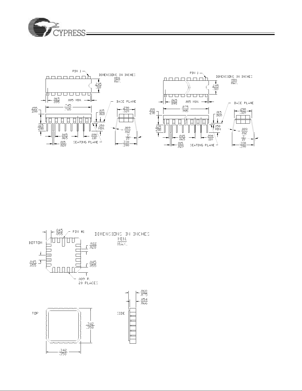
Package Diagrams
16-Lead (300-Mil) CerDIP D2
MIL-STD-1835 D-2 Con fig .A
18-Lead (300-M il) CerDIP D4
MIL-STD-18 35 D-8 Config.A
CY7C402/CY7C404
20-Pin Square Leadless Chip Carrier L61
MIL-STD-1835 C–2 A
12

CY7C401/CY7C403
Package Diagrams (continued)
16-Lead (300-Mil) Molded DIP
18-Lead (300-Mil) Molded DIP
CY7C402/CY7C404
P1
P3
© Cypress Semiconductor Corporation, 1995. The information contained herein is subject to change without notice. Cypress Semiconductor Corporation assumes no responsibility for the use
of any circ uitry other than circui try embodi ed in a Cypress Semi conductor p roduct. Nor does it convey or imply any li cense under patent or other rights . Cypress Semi conductor does not authori ze
its products for use as critical components in life-support systems where a malfunction or failure may reasonably be expected to result in significant injury to the user. The inclusion of Cypress
Semiconductor products in life-support systems application implies that the manufacturer assumes all risk of such use and in doing so indemnifies Cypress Semiconductor against all charges.
 Loading...