

f
ax id: 6139
,
CY7C374i
UltraLogic™ 128-Macrocell Flash CPLD
Features
• 128 macrocells in eight logic blocks
• 64 I/O pins
• 5 dedicated inputs including 4 clock pi ns
• In-System Reprogrammable (ISR™) Flash technology
—JTAG interface
• Bus Hold capabilities on all I/Os and dedicated inputs
• No hidden delays
• High speed
= 125 MHz
—f
MAX
= 10 ns
—t
PD
= 5.5 ns
—t
S
= 6.5 ns
—t
CO
• Fully PCI compliant
• 3.3V or 5.0V I/O operation
• Av ail able in 84-pin PLCC, 84-pin CLCC, and 100-pin
TQFP packages
• Pin compatible wit h the CY7C373i
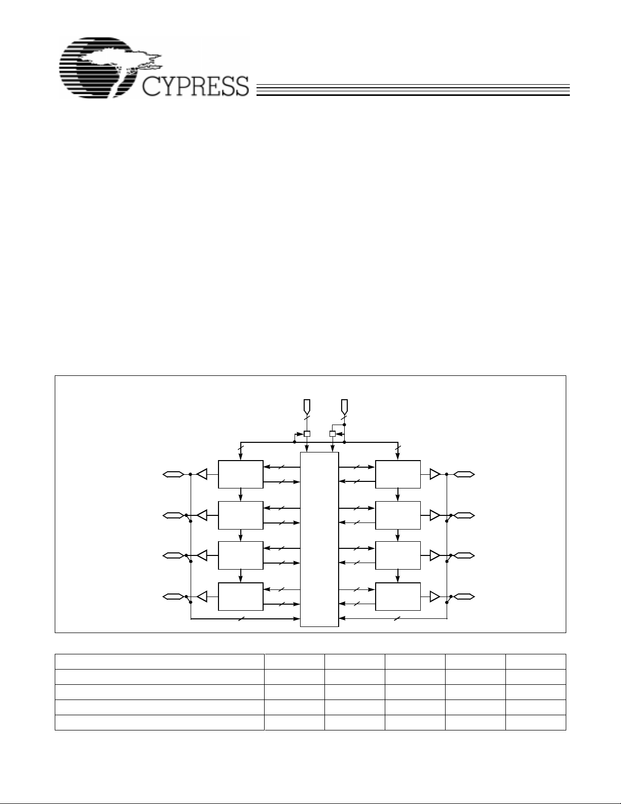
Logic Block Diagram
INPUT
MACROCELL
4 4
I/O
–I/O
0
8 I/Os
7
LOGIC
BLOCK
A
36
16
Functional Description
The CY7C374i is an In-System Reprogrammable Complex
Programmable Logic Device (CPLD) and is part of the
LASH
F
370i™ family of high-density, high-speed CPLDs. Like
all members of the F
signed to bring the eas e of use as well as PCI Local Bus Specification support and high performance of the 22V10 to
high-density CPLDs.
Like all of the UltraLogic™ F
is electrical ly e rasab l e and I n- System Rep rog ram mab le ( ISR),
which simplifies both design and manufacturing flows thereby
reducing costs. The Cypress ISR function is implemented
through a JTAG serial interface. Data is shifted in and out
through the SDI and SDO pin. The ISR interface is enabled
using the programming voltage pin (ISR
cause of the sup erior r outabi lit y of t he F
often allows users to change existing logic designs while simultaneously fixing pinout assignments.
The 128 macrocells in the CY7C374i are divided between
eigh t log ic blo cks. Each lo g i c b l o ck inc ludes 16 m a crocells, a
72 x 86 product term array, and an intelligent product term
allocator.
CLOCK
PIM
INPUTS
41
INPUT/CLOCK
MACROCELLS
36
16
INPUTS
LOGIC
BLOCK
H
LASH
370i family, the CY7C374i is de-
LASH
370i devices, the CY7C374i
). Ad ditio na lly, be-
EN
LASH
370i devi ces , ISR
8 I/Os
I/O56–I/O
63
I/O8–I/O
I/O16–I/O
I/O24–I/O
15
23
31
8 I/Os
8 I/Os
8 I/Os
LOGIC
BLOCK
B
LOGIC
BLOCK
C
LOGIC
BLOCK
D
32
36
16
36 36
16
36
16
36
16
16
36
16
LOGIC
BLOCK
G
LOGIC
BLOCK
F
LOGIC
BLOCK
E
32
8 I/Os
8 I/Os
8 I/Os
I/O48–I/O
I/O40–I/O
I/O32–I/O
55
47
39
Selection G uide
7C374i–125 7C374i–100 7C374i–83 7C374i–66 7C374iL–66
Maximum Propagation Delay
Minimum Set-Up, tS (ns) 5.5 6 8 10 10
Maximum Clock to Output
Typical Supply Current, ICC (mA) 125 125 125 125 75
Note:
1. The 3.3V I/O mode timing adder, t
Cypress Semiconductor Corporation
[1]
, tPD (ns) 10 12 15 20 20
[1]
, tCO (ns) 6.5 7 8 10 10
, must be added to this specification when V
3.3IO
CCIO
= 3.3V.
• 3901 North First Street • San Jose • CA 95134 • 408-943-2600
October 1995 – Revised December 19
7C374i-1
1997
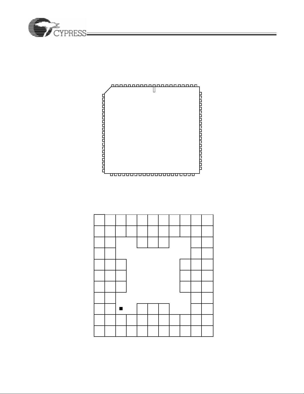
Pin Configurations
PLCC
Top View
CY7C374i
I/O
I/O
I/O10/SCLK
I/O
I/O
I/O
I/O
I/O
CLK0/I
V
GND
CLK1/I
I/O
I/O
I/O
I/O
I/O
I/O
I/O
I/O
GND
L
I/O
I/O
K
I/O
J
8
9
11
12
13
14
15
0
CCIO
1
16
17
18
19
20
21
22
23
7654321
I/O
I/O
I/O
38
I/O
28
27
I/O
I/O
I/O0V
43
42414340
2
I
31
PGA
Bottom View
I/O
31
I/O
30
I/O
29
I/O
I/O
I/O
GND
98 67 5
11
10
12
13
14
15
16
17
18
19
20
21
22
23
24
25
26
27
28
29
30
31
33
32
I/O
23
25
GND
21
I/O
22
20
3736
34
35 39 44 45
24
25
I/O
I/O
I/O27I/O28I/O29I/O30I/O
/SMODE
26
I/O
I/O
26
SMODE
I/O
24
EN
CCIO
CCINT
GND
V
ISR
84 8182 8021 79
83
GND
I/O32I/O33I/O34I/O35I/O36I/O
CCIO
CCINT
V
V
I/O
V
33
CC
I/O
I
32
2
GNDV
CC
63
62616059585756
I/O
I/O
I/O
I/O
I/O
4948
4746
37
I/O
I/O
34
I/O
I/O
35
I/O
I/O
7778 76 75
53525150
39
I/O
/SDO
38
I/O
I/O
36
GND
38
SDO
I/O40I/O
I/O
74
73
72
71
70
69
68
67
66
65
64
63
62
61
60
59
58
57
56
55
54
GND
7C374i-2
37
GND
I/O
55
I/O54/SDI
I/O
53
I/O
52
I/O
51
I/O
50
I/O
49
I/O
48
CLK3/I
GND
V
CCIO
CLK2/I
I/O
47
I/O
46
I/O
45
I/O
44
I/O
43
I/O
42
I/O
41
I/O
40
I/O
39
I/O
41
42
4
3
H
G
F
E
D
C
B
A
I/O
CLK1
/
I1
I/O
I/O
I/O
I/O
I/O
I/O
I/O
19
18
I/O
GND
16
CLK0
/I
I/O
I/O
I/O
GND
I/O
V
CC
0
I/O
14
13
11
I/O1V
CC
8
I/O
I/O
I/O
3
2
I/O
0
VCCGND
6
I/O
5
4
ISR
EN
I/O
I/O
62
61
I/O63I/O60I/O58I/O
17
15
12
10
9
7
CLK2
/I
3
V
CC
I/O
49
I/O59I/O56GND I/O
1234567891011
2
I/O43I/O
I/O46I/O
I/O45GND
I/O48CLK3
/I
I/O51I/O
I/O54I/O
SDISCLK
I/O
57
7C374i–3
44
47
4
50
52
53
55
CY7C374i
Pin Configurations
SCLK
I/O
CLK0/I
CLK1/I
(continued)
GND
I/O
8
I/O
9
I/O
10
I/O
11
I/O
12
13
I/O
14
I/O
15
0
V
CCIO
N/C
GND
1
I/O
16
I/O
17
I/O
18
I/O
19
I/O
20
I/O
21
I/O
22
I/O
23
V
CCIO
NC
CCIO
NC
V
100 9798 96
99
1
2
3
4
5
6
7
8
9
10
11
12
13
14
15
16
17
18
19
20
21
22
23
24
25
26
27 28 3029 31 32 3534 36 3833
7654321
I/O
I/O
I/O
I/O
I/O
I/O
95 94
I/O
I/O
0
CCIO
V
9091
37
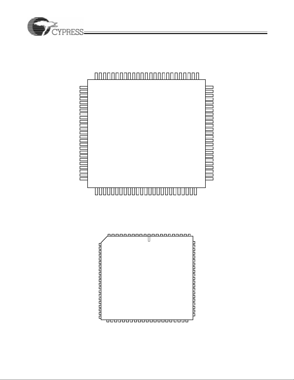
TQFP
Top View
EN
CCINT
GND
I/O
V
NC63I/O
ISR
89 88 8687 8593 92 84
4241
4039
62616059585756
I/O
I/O
I/O
I/O
I/O
I/O
83 82 81 80 79 78 77 76
43 44 45 46 48 49 50
47
GND
NC
75
74
73
72
71
70
69
68
67
66
65
64
63
62
61
60
59
58
57
56
55
54
53
52
51
SDI
V
CCIO
I/O
55
I/O
54
I/O
53
I/O
52
I/O
51
I/O
50
I/O
49
I/O
48
CLK3/I
GND
NC
V
CCIO
CLK2/I
I/O
47
I/O
46
I/O
45
I/O
44
I/O
43
I/O
42
I/O
41
I/O
40
GND
NC
4
3
I/O
I/O
I/O10/SCLK
I/O
I/O
I/O
I/O
I/O
CLK0/I
V
GND
CLK1/I
I/O
I/O
I/O
I/O
I/O
I/O
I/O
I/O
GND
GND
I/O24I/O25I/O26I/O27I/O28I/O29I/O30I/O
SMODE
GND
11
10
12
8
13
9
14
15
11
16
12
17
13
18
14
19
15
20
0
21
CC
22
23
1
24
16
17
25
18
26
27
19
28
20
21
29
22
30
31
23
33
32
34
24
I/O
2
I
31
NC
GND
CCIO
V
CLCC
Top View
7654321
I/O
43
31
42414340
2
I
VCCI/O0V
VCCV
GND
GND
I/O
I/O
I/O
I/O
I/O
I/O
98 67 5
3736
38
35 39 44 45
25
I/O
I/O27I/O28I/O29I/O30I/O
/SMODE
26
I/O
I/O32I/O33I/O34I/O35I/O36I/O37I/O38I/O
CCINT
V
EN
63
62616059585756
CC
I/O
I/O
I/O
ISR
84 8182 8021 79
83
4948
4746
CC
I/O32I/O33I/O34I/O35I/O36I/O
I/O
37
I/O
I/O
7778 76 75
I/O
/SDO
38
I/O
39
I/O
74
73
72
71
70
69
68
67
66
65
64
63
62
61
60
59
58
57
56
55
54
53525150
39
GND
7C374i-2
V
I/O
CCIO
SDO
GND
I/O
I/O54/SDI
I/O
I/O
I/O
I/O
I/O
I/O
CLK3/I
GND
V
CLK2/I
I/O
I/O
I/O
I/O
I/O
I/O
I/O
I/O
7C374i-4
55
53
52
51
50
49
48
4
CC
3
47
46
45
44
43
42
41
40
3

CY7C374i
Functional Description
The logic blocks in the F
(continued)
LASH
370i architecture are connected
with an extremely fast and predictable routing resource—the
Programmab le Int erconnect Matrix (PIM). T he PIM brings f lexibility, routability, speed, and a uniform delay to the interconnect.
Like all members of the F
LASH
370i fami ly, the CY7C374i is rich
in I/O resources. Every two macrocells in the device feature
an associated I/O pin, resulting in 64 I/O pins on the
CY7C374i. In addition, there is one dedicated input and four
input/cl ock pins.
Finally, the CY7C374i features a very simple timing model.
Unlike other high-density CPLD architectures, there are no
hidden speed delays such as fanout effects, interconnect delays, or expander delays. Regardless of the number of resources used or t he type of appli cation , the ti ming par amet ers
on the CY7C374i remain the same.
Logic Block
The number of logic blocks distinguishes the members of the
LASH
F
370i family. The CY7C374i includes eight logic blocks.
Each logic bl ock is cons tructed of a product term array, a product term allocator, and 16 macrocells.
Product Term Array
The product term array in the F
LASH
370i logic block includes
36 inputs from the PIM and outputs 86 product terms to the
product term allocator. The 36 inputs from the PIM are available in both positive and negative polarity, making the overall
array size 72 x 86. This large array in each logic block allows
for v ery com ple x f uncti ons t o be implement ed in si ngle p asses
through the device.
Product Term Allocator
The product term allocator is a dynamic, configur able resourc e
that shifts product terms to macrocells that require them. Any
number of pr oduct terms between 0 and 16 inclusive can be
assigned to any of the logic block macrocells (this is called
product term steering). Furthermore, product terms can be
shared among multiple macrocells. This means that product
terms that are c ommon t o more tha n one output c an be implemented in a single product term. Product term steering and
product term sharing help to increase the effective density of
LASH
the F
370i CPLDs. Note that product term allocation is
handled by soft ware and is invisible to the user.
I/O Macrocell
Half of the macrocells on the CY7C374i have I/O pins associated with them. The input to the macrocell is the sum of between 0 and 16 product terms from th e product term allo cator.
The I/O macrocell includes a register that can be optionally
bypassed, polarity control over the input sum-term, and two
global clocks to trigger the register. The macrocell also features a separate feedback path to the PIM so that the register
can be buried if the I/ O pin i s used as an input.
Buried Macrocell
The buried macrocell is very similar to the I/O macrocell.
Again, it includes a register that can be configured as combinatorial, as a D flip-flop, a T flip-flop, or a latch. The clock for
this register has the same options as described for the I/O
macrocell. O ne difference on the buried macrocell is the addition of i nput register capability. The user can program the buried macrocell to act as an input register (D-type or latch)
whose input comes fro m the I/O pin associate d with the neigh-
boring macrocell. The output of all buried macrocells is sent
directly to the PIM reg ardless of its configur ation.
Programmable Interconnect Matrix
The Programmable Interconnect Matrix (PIM) connects the
eight logic blocks on the CY7C374i to the inputs and to each
other. All inputs (including feedbacks) travel through the PIM.
There is no speed penalty incurred by signals traversing the
PIM.
Programming
For an overview of ISR programming, refer to the F
LASH
370i
Family data sheet and for ISR cable and software specifications, refer to ISR data sheets. For a detailed description of
ISR capabilities, refer to the Cypress application note, “An Introduction to In System Reprogramming with F
LASH
370i.”
PCI Compliance
LASH
The F
370i f amily of CMOS CPLDs are ful ly compliant with
the PCI Local Bus Specification published by the PCI Special
Interest Group. The simple and predictable timing model of
LASH
F
370i ensures co mplianc e wi th the PCI A C spe cifi cati ons
independent of the design. On the other hand, in CPLD and
FPGA architectur es without simple and predi ctable timing, PCI
compliance is dependent upon routing and product term distribution.
3.3V or 5.0V I/O Operati on
LASH
The F
and 5.0V systems. All de vices ha v e t wo sets of V
set, V
another set, V
370i fami ly can be conf igured to operate in both 3.3V
CC
CCINT
, for internal operation and input buffers, and
CCIO
, for I/O output drivers. V
CCINT
pins m ust
pins: one
always be connected to a 5.0V power supply. However, the
CCIO
V
pins may be connected to either a 3.3V or 5.0V power
supply, depending on the output requirements. When V
CCIO
pins are connec ted t o a 5 .0V sour ce , the I/O v o ltage le v els a re
compatible with 5.0V systems. When V
CCIO
pins are
connected to a 3.3V source, the input voltage levels are
compatible with both 5. 0V and 3.3V systems , while the output
voltage le vel s are compatibl e with 3.3V sys tems. There will be
an additional ti ming del a y on al l ou tput b uffers when operating
in 3.3V I/O mode. The added flexibility of 3.3V I/O capability
is avail able in commercial and industrial temperature ranges.
Bus Hold Capabilities on all I/Os and Dedicated Inputs
In addition to ISR c apabil ity, a new f eatur e call ed b us-ho ld has
been added to all F
LASH
370i I/Os and dedicated input pins.
Bus-hold, whi ch is an improved v ersion of the popular internal
pull-up re sistor, is a weak l atch connect ed to the pin that does
not degrade the device’s performance. As a latch, bus-hold
recalls the last state of a pin when it is three-stated, thus reducing system noise in bus-interface applications. Bus-hold
additionally a llo ws un used de vi ce pins t o rem ain uncon nected
on the board, which is particularly useful during pro totyping as
designers can route new signals to the device without cutting
trace connections to V
or GND.
CC
Design Tools
Development software f or the CY7C371i is av ailable from Cypress’s
Warp2
®,
Warp2
Sim™, and
Warp3
® software packa ges. All of these products are based on the IEEE-standard
VHDL language. Cypr ess also activ ely supports third-pa rty design tools from companies such as Synopsys, Mentor Graphics, Cadence , and Synario . Please r efer t o third-party tool su pport for further information.
4
CY7C374i
Maximum Ratings
Static Discharge Voltage ...........................................>2001V
(per MIL-STD-883, Method 3015)
(Abov e which the useful lif e m ay be impaired. For user guidelines, not tested.)
Storag e Temperature ...... ... ....... .. ...............–6 5°C to +150°C
Ambient Temperature with
Power Applied.............................................–55°C to +125°C
Supply Voltage to Ground Potential......... .. ....–0.5V to +7.0V
DC Voltage Applied to Outputs
in High Z State ............................................... –0.5V to +7.0V
DC Input Voltage............................................ –0.5V to +7.0V
DC Program Voltage .....................................................12.5V
Output C ur re n t in to O u tp u ts.............. ... .. ........ .. ............16 m A
Electrical Characteristics
Over the Operati ng Range
Latch-Up Current .....................................................>200 mA
Operating Range
Ambient
Range
Temperature
Commercial 0°C to +70°C 5V ± .25V 5V ± .25V
−40°C to +85°C
–55°C to +125°C 5V ± .5V
[3, 4]
Industrial
[2]
Military
V
CC
V
CCINT
5V ± .5V 5V ± .5V
V
CCIO
OR
3.3V ± .3V
OR
3.3V ± .3V
Parameter Description Te st Conditions Min. Typ. Max. Unit
V
OH
Output HIGH Voltage VCC = Min. IOH = –3.2 mA (Com’l/Ind)
[5]
2.4 V
IOH = –2.0 mA (Mil) V
V
V
OHZ
OL
Output HIGH Voltage
with Output Disabl ed
VCC = Max. IOH = 0 µA (Com’l/Ind)
[9]
IOH = –50 µA (Com’l/Ind)
Output LOW Voltage VCC = Min. IOL = 16 mA (Com’l/Ind)
[5, 6]
[5]
[5, 6]
4.0 V
3.6 V
0.5 V
IOL = 12 mA (Mil) V
V
IH
V
IL
I
IX
I
OZ
I
OS
I
CC
Input HIGH Voltage Guaranteed Inp ut Logical HIGH v oltage f or al l inputs
Input LOW Voltage Guaranteed Input Logica l LO W v olta ge f or al l inp uts
Input Load Current VI = Internal GND, VI = V
CC
Output Leakage Current VCC = Max., VO = GND or VO = VCC, Output Disab led –50 +50
VCC = Max., VO = 3.3V, Output Disabled
Output Short
Circuit Current
[8, 9]
VCC = Max., V
Power Supply Current VCC = Max., I
f = 1 MHz, VIN = GND, V
= 0.5V –30 –160 mA
OUT
= 0 mA, Com’ l/ Ind. 125 200 mA
OUT
CC
[10]
[6]
Com’l “L” –66 75 125 mA
[7]
2.0 7.0 V
[7]
–0.5 0.8 V
–10 +10
0 –70 –125
µA
µA
µA
Military 125 250 mA
I
BHL
I
BHH
I
BHLO
I
BHHO
Notes:
2. T
is the “instant on” case temperature.
A
3. See the last page of this specification for Group A subgroup testing information.
4. If V
5. IOH = –2 mA, IOL = 2 mA for SDO.
6. When the I/O is three-stated, the bus-hold circuit can weakly pull the I/O to a maximum of 4.0V if no leakage current is allowed. This voltage is lowered significantly
by a small leakage current. Note that all I/Os are three-stated during ISR programming. Refer to the application note “Understanding Bus Hold” for additional
information.
7. These are absolute values with respect to device ground. All overshoots due to system or tester noise are included.
8. Not more than one output should be tested at a time. Duration of the short circuit should not exceed 1 second. V
problems caused by tester ground degradation.
9. Tested initially and after any design or process changes that may affect these parameters.
10. Measured with 16-bit counter programmed into each logic block.
Input Bus Hold LOW
VCC = Min., VIL = 0.8V +75
Sustaining Current
Input Bus Hold HIGH
VCC = Min., VIH = 2.0V –75
Sustaining Current
Input Bus Hold LOW
VCC = Max. +500
Overdrive Current
Input Bus Hold HIGH
VCC = Max. –500
Overdrive Current
is not specified, the device can be operating in either 3.3V or 5V I/O mode; VCC=V
CCIO
CCINT
.
= 0.5V has been chosen to avoid test
OUT
µA
µA
µA
µA
5

CY7C374i
Capacitance
[9]
Parameter Description Tes t Condi tions Min. Max. Unit
[11, 12]
C
I/O
C
CLK
Inductance
[9]
Parameter Description Test Conditions 100-PinTQFP
Input Capacitance VIN = 5.0V at f=1 MHz 8 pF
Clock Signal Capacitance VIN = 5.0V at f = 1 MHz 5 12 pF
84-Lead
PLCC
84-Lead
CLCC Unit
L Maximum Pin Inductance VIN = 5.0V at f = 1 MHz 8 8 5 nH
Endurance Characteristics
[9]
Parameter Description Test Conditions Max. Unit
N Maximum Reprogramming Cycles Normal Programming Conditions 100 Cycles
AC Test Loads and Waveforms
5 pF
238Ω(COM'L)
319Ω(MIL)
170Ω(COM'L)
236Ω(MIL)
7C374i-5
3.0V
GND
<2ns
ALL INPUT PULSES
90%
10%
(c)
90%
10%
7C374i-6
5V
OUTPUT
INCLUDING
JIG AND
SCOPE
238Ω(COM'L)
35 pF
319Ω(MIL)
170Ω(COM'L)
236Ω(MIL)
5V
OUTPUT
INCLUDING
JIG AND
SCOPE
(a) (b)
<2ns
Equivalent to: THÉ VENIN EQUIVALENT
99Ω(COM'L)
OUTPUT
Parameter
t
ER(–)
t
ER(+)
t
EA(+)
t
EA(–)
136Ω(MIL)
[13]
1.5V
2.6V
1.5V
V
X
V
thc
2.08V (COM'L)
2.13V (MIL)
Output Wav eform Measurement Level
V
OH
–0.5V
–0.5V
V
OH
–0.5V
V
X
V
X
–0.5V
V
X
V
X
V
OH
V
OH
Notes:
11. C
for the CLCC package are 12 pF Max
I/O
12. C
for dedicated Inputs, and for I/O pins with JT AG functionality is 12 pF Max., and for ISREN is 15 pF Max.
I/O
measured with 5-pF AC Test Load and tEA measured with 35-pF AC Test Load.
13. t
ER
6
CY7C374i
Switching C h aracteri sti cs
Over the Operating Range
[14]
7C374i–66
7C374i–125 7C374i–100 7C374i–83
7C374iL–66
Parameter Description Min. Max. Min. Max. Min. Max. Min. Max. Unit
Combinatorial Mode Parameters
t
PD
t
PDL
t
PDLL
t
EA
t
ER
Input to Combinato rial Ou tput
Input to Ou tput Thro ugh Transparent I nput o r
Output Latch
Input to Output Through Transparent Input
and Output Latches
[1]
[1]
Input to Output Enab le
Input to Output Disab le 14 16 19 24 ns
[1]
10 12 15 20 ns
13 15 18 22 ns
15 16 19 24 ns
[1]
14 16 19 24 ns
Input Registered/Latched Mode Parameters
[1]
[9]
[9]
3 3 4 5 ns
3 3 4 5 ns
14 16 19 24 ns
16 18 21 26 ns
t
WL
t
WH
t
IS
t
IH
t
ICO
t
ICOL
Clock or Latch Enable Input LOW Time
Clock or Latch Enab le Input HIGH Time
Input Register or Latch Set-Up Time 2 2 3 4 ns
Input Register or Latch Hold Time 2 2 3 4 ns
Input Regist er Cl ock or Latch En ab le t o Com-
binatorial Output
[1]
Input Register Clock or Latch Enable to Output Through Transparent Output Latch
Output Registered/ Latched Mode Parame ters
t
CO
t
S
t
H
t
CO2
t
SCS
t
SL
Clock or Latch Enable to Output
Set-Up Time from Input to Clock or Latch En-
able
Register or Latch Data Hold Time 0 0 0 0 ns
Output Clock or Latch Enab le to Output Dela y
(Through Memory Array)
Output Clock or Latch Enable to Out put Clock
or Latch Enable (Through Memory Array)
Set-Up Time f rom Input Through Transparent
Latch to Output Register Clock or Latch En-
[1]
6.5 7 8 10 ns
5.5 6 8 10 ns
[1]
14 16 19 24 ns
8 10 12 15 ns
10 12 15 20 ns
able
t
HL
Hold Time for In put Through Transparent
Latch from Output Regi ster Clock or Latch
0
0 0 0 ns
Enable
f
MAX1
f
MAX2
f
MAX3
tOH–t
37x
IH
Maximum Frequency with Inte rnal F eedback
(Least of 1/t
, 1/(tS + tH), or 1/tCO)
SCS
[9]
Maximum Frequency Data P ath in Output
Registered/L atched Mode (Lesser of 1/(t
t
), 1/(tS + tH), or 1/tCO)
WH
WL
+
Maximum Frequency with External Feedback
(Lesser of 1 /(t
Output Data Stab le f rom Out put Cl oc k Minus
Input Register Hold Time for 7C37x
+ tS) and 1/(tWL + tWH))
CO
[9, 15]
125 100 83 66 MHz
158.3
83.3
143 125 100 MHz
76.9 67.5 50 MHz
0 0 0 0 ns
Pipelined Mode Parameters
t
ICS
f
MAX4
Notes:
14. All AC parameters are measured with 16 outputs switching and 35-pF AC Test Load.
15. This specification is intended to guarantee interface compatibility of the other members of the CY7C370i family with the CY7C374i. This specification is met
for the devices operating at the same ambient temperature and at the same power supply voltage.
Input Regist er Clock to O utput Regist er Clock 8 10 12 15 ns
Maximum Frequency in Pipelined M ode
(Least of 1/(t
1/(t
+ tIH), or 1/t
IS
+ tIS), 1/t
CO
SCS
ICS
)
, 1/(tWL + tWH),
125
100 83.3 66.6 MHz
7

CY7C374i
Switching C h aracteri sti cs
Over the Operating Range
[14]
(continued)
7C374i–66
7C374i–125 7C374i–100 7C374i–83
7C374iL–66
Parameter Description Min. Max. Min. Max. Min. Max. Min. Max. Unit
Reset/Preset Parameters
t
t
t
t
t
t
RW
RR
RO
PW
PR
PO
Asynchronous Reset Width
Asynchronous Reset Recovery Time
Asynchronous Reset to Output
Asynchronous Preset Width
Asynchronous Preset Recovery Time
Asynchronous Preset to Output
[9]
[9]
[1]
[9]
[9]
[1]
10 12 15 20 ns
12 14 17 22 ns
16 18 21 26 ns
10 12 15 20 ns
12 14 17 22 ns
16 18 21 26 ns
T ap Controller Parameter
f
TAP
Tap Controller Frequ ency 500 500 500 500 kHz
3.3V I/O Mode Parameters
t
3.3IO
3.3V I/O mode timing adder 1 1 1 1 ns
Switching Waveform s
Combinatorial Output
INPUT
t
COMBINATORIAL
OUTPUT
PD
7C374i-7
Registered Output
INPUT
CLOCK
REGISTERED
OUTPUT
CLOCK
LatchedOutput
INPUT
LATCH ENABLE
LATCHED
OUTPUT
t
PDL
t
S
t
WH
t
S
t
H
t
H
t
CO
t
WL
7C374i-8
t
CO
7C374i-9
8

CY7C374i
Switching Waveform s
Registered Input
REGISTERED
INPUT
INPUT REGISTER
COMBINATORIAL
LatchedInput
LATCHED INPUT
LATCH
CLOCK
OUTPUT
CLOCK
ENABLE
(continued)
t
ICO
t
WL
t
IH
7C374i-10
t
IS
t
WH
t
IS
t
IH
COMBINATORIAL
OUTPUT
LATCH ENABLE
LatchedInput and Output
LATCHED INPUT
LATCHED
OUTPUT
INPUT LATCH
ENABLE
OUTPUT LATCH
ENABLE
t
PDL
t
ICOL
t
ICO
t
WH
t
ICS
t
WL
7C374i-11
t
PDLL
t
SL
t
HL
LATCH ENABLE
t
WH
t
WL
7C374i-12
9
CY7C374i
Switching Waveform s
Asynchronous Reset
INPUT
REGISTERED
OUTPUT
CLOCK
AsynchronousPreset
INPUT
REGISTERED
OUTPUT
(continued)
t
RW
t
RO
t
RR
7C374i-13
t
PW
t
PO
CLOCK
Output Enable/Disable
INPUT
OUTPUTS
t
PR
7C374i-14
t
ER
t
EA
7C374i-16
10

Ordering Informati on
CY7C374i
Speed
(MHz)
Ordering Code
Package
Name
Package Type
Operating
Range
125 CY7C374i–125AC A100 100-Pin Thin Quad Flat Pack Commercial
CY7C374i–125JC J83 84-Lead Plastic Leaded Ch ip Carrier
100 CY7C374i–100AC A100 100-Pin Thin Quad Flat Pack Commercial
CY7C374i–100JC J83 84-Lead Plastic L eaded Chip Carrier
83 CY7C374i–83A C A100 100-Pin Thin Quad Flat Pack Commercial
CY7C374i–83JC J83 84-Lead Plastic L eaded Chip Carrier
CY7C374i–83AI A10 0 100-Pin Thin Quad Flat Pack Industrial
CY7C374i–83JI J83 84-Lead Plastic L eaded Chip Carri er
CY7C374i-83GMB G84 84-Pin Ceramic Pin Grid Array Military
CY7C374i–83YMB Y84 84-Pi n Ceramic Leade d Chip Carrier
66 CY7C374i–66A C A100 100-Pin Thin Quad Flat Pack Commercial
CY7C374i–66JC J83 84-Lead Plastic L eaded Chip Carrier
CY7C374i–66AI A10 0 100-Pin Thin Quad Flat Pack Industrial
CY7C374i–66JI J83 84-Lead Plastic L eaded Chip Carri er
CY7C374i-66GMB G84 84-Pin Ceramic Pin Grid Array Military
CY7C374i–66YMB Y84 84-Pi n Ceramic Leade d Chip Carrier
CY7C374iL–66AC A100 100-Pin Thin Quad Flat Pack Commercial
CY7C374iL–66JC J83 84-Lead Plastic L eaded Chip Carrier
MILITARY SPECIFICATIONS
Group A Subgroup T esti ng
DC Characteristics
Parameter Subgroups
V
OH
V
OL
V
IH
V
IL
I
IX
I
OZ
I
CC1
ISR, UltraLogic, F
Warp2
and
Warp3
1, 2, 3
1, 2, 3
1, 2, 3
1, 2, 3
1, 2, 3
1, 2, 3
1, 2, 3
LASH
370, F
LASH
370i, and
are registered trademarks of Cypress Semiconductor Corporation.
Switching Characteristics
Parameter Subgroups
t
PD
t
PDL
t
PDLL
t
CO
t
ICO
t
ICOL
t
S
t
SL
t
H
t
HL
t
IS
t
IH
t
ICS
t
EA
t
ER
Document #: 38-00496-C
Warp2
Sim are trademarks of Cypress Semiconductor Corporat ion.
9, 10, 11
9, 10, 11
9, 10, 11
9, 10, 11
9, 10, 11
9, 10, 11
9, 10, 11
9, 10, 11
9, 10, 11
9, 10, 11
9, 10, 11
9, 10, 11
9, 10, 11
9, 10, 11
9, 10, 11
11
Package Diagrams
CY7C374i
100-PinThin Quad Flat Pack A100
84-Pin Grid Arr ay (Cavi ty Up) G84
12
CY7C374i
Package Diagrams
(continued)
84-LeadPlastic Leaded Chip Carrier J83
84-Pin Ceramic Leaded Chip Carrier
Y84
© Cypress Semiconductor Corporation, 1997. The information contained herein is subject to change without notice. Cypress Semiconductor Corporation assumes no responsibility for the use
of any circuitry other than circuitry embodied in a Cypress Semiconductor product. Nor does it con vey or imply any l icense under patent or other rights. Cypress Semi conductor does not authorize
its products for use as critical components in life-support systems where a malfunction or failure may reasonably be expected to result in significant injury to the user. The inclusion of Cypress
Semiconductor products in life-support systems application implies that the manufacturer assumes all risk of such use and in doing so indemnifies Cypress Semiconductor against all charges.
WWW.ALLDATASHEET.COM
Copyright © Each Manufacturing Company.
All Datasheets cannot be modified without permission.
This datasheet has been download from :
www.AllDataSheet.com
100% Free DataSheet Search Site.
Free Download.
No Register.
Fast Search System.
www.AllDataSheet.com
 Loading...