

Page 1
92A
CY7C291A
Features
•
Windowed for reprogrammability
•
CMOS for optimum speed/power
•
High speed
—
20 ns (commercial)
—
25 ns (military)
•
Low power
—
660 mW (commercial and military)
•
Low standby power
—
220 mW (commercial and military)
•
EPROM technology 100% programmable
•
Slim 300-mil or standard 600-mil packaging available
•
5V ±10% VCC, commercial and military
•
TTL-compatible I/O
•
Direct replacement for bipolar PROMs
•
Capable of withstanding >2001V static discharge
Functional Description
CY7C292A/CY7C293A
2K x 8 Reprogrammable PROM
identical, bu t are pac ka ged in 300 -mil (7C29 1A, 7C293A) an d
600-mil wide plastic and hermetic DIP packages (7C292A).
The CY7C293A has an automatic power down feature which
reduces the power consumption by over 70% when deselected. The 300-mil ceramic package may be equipped with an
erasure window; when exposed to UV light the PROM is
erased and can then be reprogr ammed. The memo ry cells utilize prov en EPR OM floatin g-gate techno log y and b yte-wide intelligent programming algorithms.
The CY7C291A, CY7C292A, and CY7C293A are plug-in replacements for bipolar devices and offer the advantages of
lower power, reprogrammability, superior performance and
programming yield. The EPROM cell requires only 12.5V for
the supervoltage and low current requirements allow for gang
programming . The EPROM cells allow for each memory location to be tested 100%, as each location is written into , erased,
and repeatedly exercised prior to encapsulation. Each PROM
is also tested for AC performance to guarantee that after customer programming the product will meet DC and AC specification limits.
A read is accomplished by placing an active LOW signal on
, and active HIGH signals on CS2 and CS3. The contents
CS
1
of the memory location addressed by the address line (A
) will become available on the output lines (O0 − O7).
A
10
−
0
The CY7C291A, CY7C2 92A, an d CY7C2 93A are high-pe rf ormance 2K-word b y 8-bit CMOS PR OMs . The y are functi onally
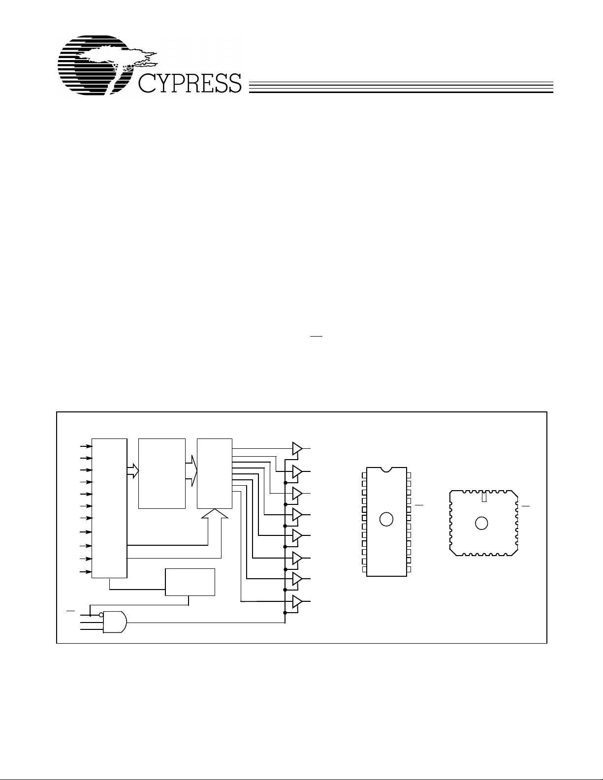
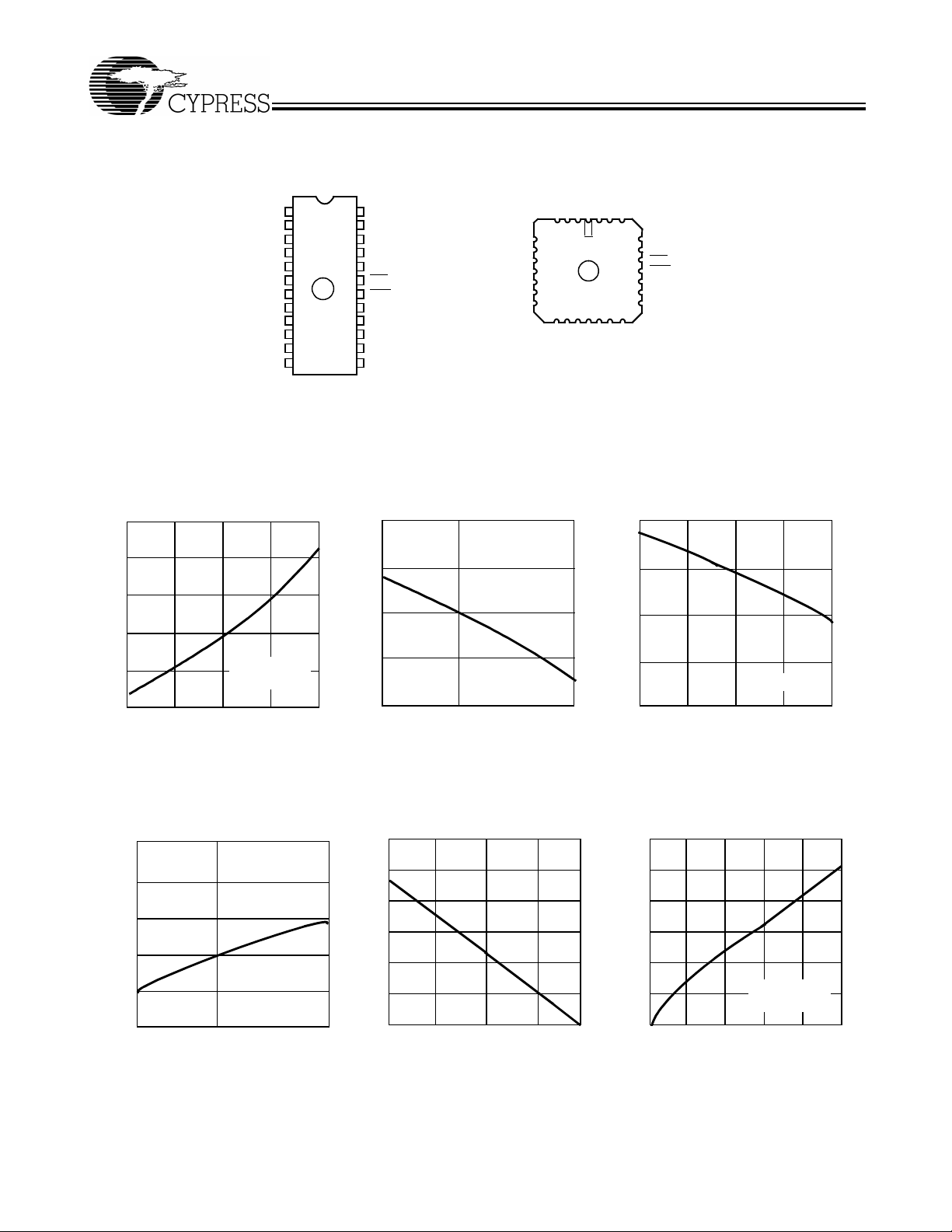
LogicBlock Diagram Pin Configurations
A
CS
CS
CS
A
0
A
1
A
2
A
3
A
4
A
5
A
6
A
7
A
8
A
9
10
1
2
3
ROW
ADDRESS
ADDRESS
DECODER
COLUMN
ADDRESS
PROGRAM-
MABLE
ARRAY
POWER
DOWN
7C293A
MULTI-
PLEXER
O
7
O
6
O
5
O
4
O
3
O
2
O
1
O
0
C291A-1
GND
A
7
A
6
A
5
A
4
A
3
A
2
A
1
A
0
O
0
O
1
O
2
DIP
Top View
1
2
3
7C291A
7C292A
4
7C293A
5
6
7
8
9
10
11 14
12 13
24
23
22
21
20
19
18
17
16
15
C291A-2
V
A
A
A
CS
CS
CS
O
O
O
O
O
LCC/PLCC (Opaque Only)
Top View
CC
8
9
10
1
2
3
7
6
5
4
3
NC
5
7
A
A6A
321 27
4
A
5
4
A
6
7C291A
3
A
2
7
A
1
8
A
9
0
7C293A
10
O
11
0
1314151617
12
2
1
O
O
GND
Window available on
7C291A and7C293A
only.
NC
NC
9
CC
V
A8A
28
26
A
25
10
CS
24
1
CS
23
2
CS
3
22
21
NC
O
20
7
19
O
6
18
5
3
O4O
O
C291A-3
Cypress Semiconductor Corporation
• 3901 North First Street • San Jose • CA 95134 • 408-943-2600
March 1986 – Revised May 1993
Page 2

CY7C291A
CY7C292A/CY7C293A
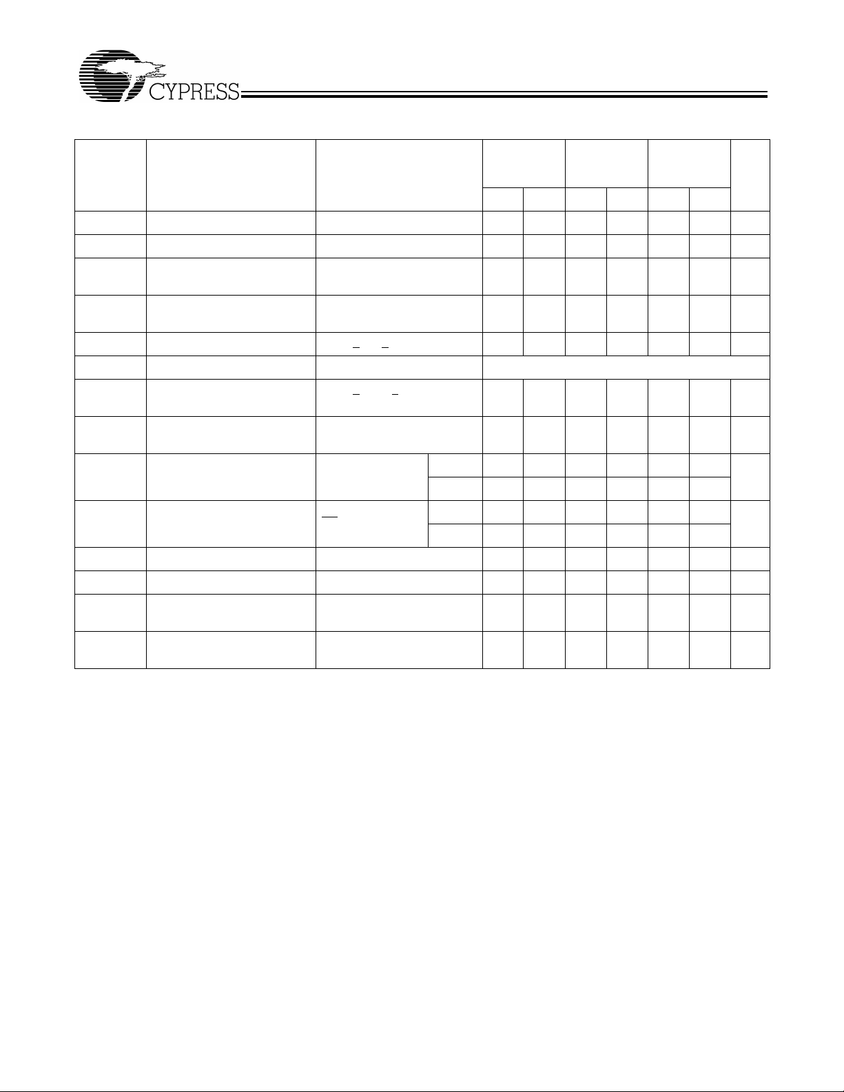
Selection Guide
7C291A-25
7C292A-25
7C293A-25
7C291A-20
7C292A-20
7C293A-20
7C291AL-25
7C292AL-25
7C293AL-25
Maximum Access Time (ns) 20 25 35 50
Maximum Operating
Current (mA)
Standard Commercial 120 90 90 90
Military 120 90 90
L Commercial 60 60 60
Standby Current (mA)
7C293A Only
Maximum Ratings
(Above wh ich the usefu l life may be impai red. F or us er guid e-
Commercial 40 30 30 30
Military 40 40 40
Latch-Up Current.....................................................>200 mA
Operating Range
lines, not tested.)
Storage Temperature ......................................−65°C to+150°C
Ambient Temperature with
Po wer Applied...................................................−55°C to+125°C
Supply Voltage to Ground Potential...................−0.5V to+7.0V
DC Voltage Applied to Outputs
in High Z State......................................................−0.5V to+7.0V
DC Input Voltage .................................................−3.0V to +7.0V
DC Program Voltage.....................................................13.0V
UV Exposure.................................................7258 Wsec/cm
2
Range
Commercial 0°C to + 70°C 5V ±10%
Industrial
Military
Notes:
1. Contact a Cypress representative for industrial temperature range spec-
2. T
[1]
[2]
ifications.
is the “instant on” case temperature.
A
Static Discharge Voltage............................................>2001V
(per MIL-STD-883, Method 3015)
7C291A-35
7C292A-35
7C293A-35
7C291AL-35
7C292AL-35
7C293AL-35
7C291A-50
7C292A-50
7C293A-50
7C291AL-50
7C292AL-50
7C293AL-50
Ambient
Temperature V
−40°C to + 85°C 5V ±10%
−55°C to + 125°C 5V ±10%
CC
2
Page 3
CY7C291A
CY7C292A/CY7C293A
7C291A-25
7C292A-25
7C293A-25
7C291AL-25
7C292AL-25
7C293AL-25
Electrical Characteristics
Over the Operating Range
[3,4]
7C291A-20
7C292A-20
7C293A-20
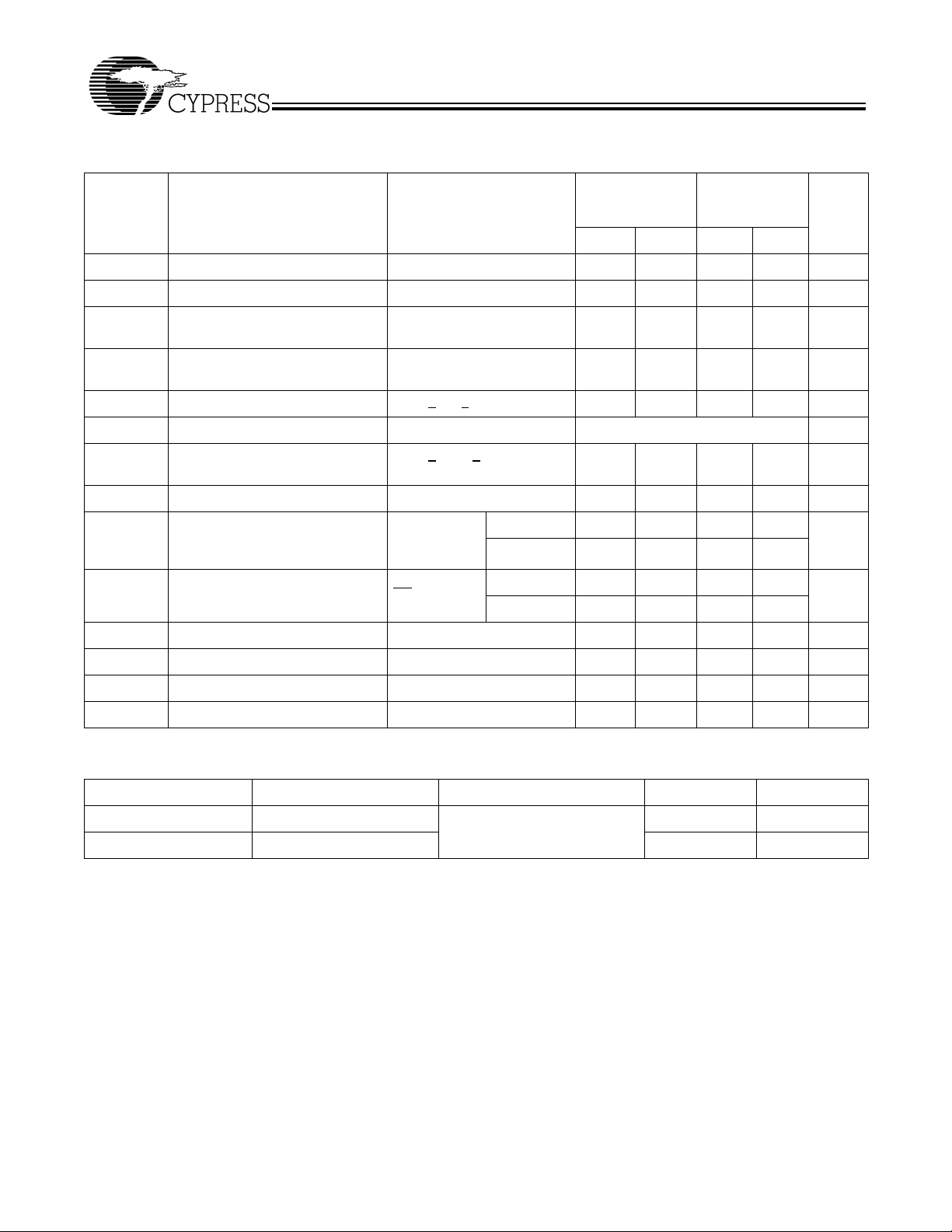
Parameter Description T est Conditions Min. Max. Min. Max. Min. Max. Unit
V
OH
V
OL
V
IH
V
IL
I
IX
V
CD
I
OZ
I
OS
I
CC
Output HIGH Voltage VCC = Min., IOH = −4.0 mA 2.4 2.4 2.4 V
Output LOW Voltage VCC = Min., IOL = 16.0 mA 0.4 0.4 0.4 V
Input HIGH Voltage Guaranteed Input Logical
HIGH Vo ltage for All Inputs
Input LOW Voltage Guaranteed Input Logical
2.0 V
CC
2.0 V
CC
2.0 V
CC
0.8 0.8 0.8 V
LOW Voltage for All Inputs
Input Load Current GND < VIN < V
CC
−10 +10 −10 +10 −10 +10 µA
Input Diode Clamp Voltage Note 4
Output Leakage Current GND < V
Output Disabled
Output Short Circuit
Current
[5]
VCC Operating Supply
Current
VCC = Max., V
VCC = Max.,
I
= 0 mA
OUT
OUT
< VCC,
= GND −20 −90 −20 −90 −20 −90 mA
OUT
−10 +10 −10 +10 −10 +10 µA
Com’l 120 90 60 mA
Mil 120
V
I
SB
V
PP
I
PP
V
IHP
V
ILP
Notes:
3. See the last page of this specification for Group A subgroup testing information.
4. See the “Introduction to CMOS PROMs” section of the Cypress Data Book for general information on testing.
5. For test purposes, not more than one output at a time should be shorted. Short circuit test duration should not exceed 30 seconds.
Standby Supply Current
(7C293A Only)
VCC = Max.,
= V
CS
1
IH
Com’l 40 30 30 mA
Mil 40
Programming Supp ly Voltage 12 13 12 13 12 13 V
Programming Supply Current 50 50 50 mA
Input HIGH Programm in g
3.0 3.0 3.0 V
Voltage
Input LOW Progr a mm in g
0.4 0.4 0.4 V
Voltage
3
Page 4
CY7C291A
CY7C292A/CY7C293A
7C291A-35, 50
7C292A-35, 50
7C293A-35, 50
Electrical Characteristics
Over the Operating Range
[3,4]
(continued)
7C291AL-35, 50
7C292AL-35, 50
7C293AL-35, 50
Parameter Description Test Conditions Min. Max. Min. Max. Unit
V
OH
V
OL
V
IH
V
IL
I
IX
V
CD
I
OZ
I
OS
I
CC
I
SB
Output HIGH Voltage VCC = Min., IOH = −4.0 mA 2.4 2.4 V
Output LOW Voltage VCC = Min., IOL = 16.0 mA 0.4 0.4 V
Input HIGH Voltage Guaranteed Input Logical
2.0 2.0 V
HIGH Vo ltage for All Inputs
Input LOW Voltage Guaranteed Input Logical
0.8 0.8 V
LOW Voltage for All Inputs
Input Load Current GND < VIN < V
CC
−10 +10 −10 +10 µA
Input Diode Clamp Voltage Note 4
Output Leakage Current GND < V
Output Disabled
Output Short Circuit Current
[5]
VCC = Max., V
VCC Operating Supply Current VCC = Max.,
VIN = 2.0V
=0 mA
I
OUT
Standby Supply Current
(7C293A Only)
VCC = Max.,
=V
CS
1
OUT
< VCC,
= GND −20 −90 −20 −90 mA
OUT
−10 +10 −10 +10 µA
Commercial 60 90 mA
Military 90
Commercial 30 30 mA
IH
Military 40
V
PP
I
PP
V
IHP
V
ILP
Capacitance
Parameter Description Test Conditions Max. Unit
C
IN
C
OUT
Programming Supply Voltage 12 13 12 13 V
Programming Supply Current 50 50 mA
Input HIGH Programm in g Voltage 3.0 3.0 V
Input LOW Programming Voltage 0.4 0.4 V
[4]
Input Capacitance TA = 25°C, f = 1 MHz,
V
= 5.0V
Output Capacitance 10 pF
CC
10 pF
4
Page 5
CY7C291A
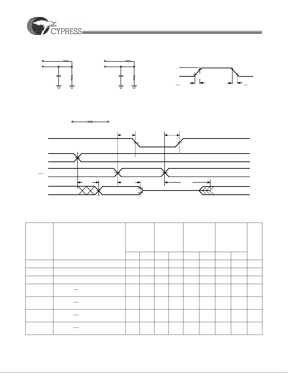
AC Test Loads and Waveforms
Ω
5V
OUTPUT
30pF
INCLUDING
JIG AND
SCOPE
R1250
R2
167
Ω
[4]
5V
OUTPUT
5pF
INCLUDING
JIG AND
SCOPE
(a) NormalLoad (b) HighZ Load
Equivalent to: THÉ VENINEQUIVALENT
Ω
100
V
CC
SUPPLY
CURRENT
−
A
A
0
10
ADDRESS
OUTPUT 2.0V
Ω
R1250
3.0V
R2
Ω
167
C291A-4 C291A-5
C291A-6
t
PD
50% 50%
GND
<5ns <5ns
t
PU
CY7C292A/CY7C293A
ALL INPUT PULSES
90%
10%
90%
10%
−
CS
CS
2
3
CS
1
t
AA
O
-O
0
7
Switching Characteristics
Over the Operating Range
t
HZCS
[3, 4]
7C291A-20
7C292A-20
7C293A-20
7C291A-25
7C292A-25
7C293A-25
7C291AL-25
7C292AL-25
7C293AL-25
t
ACS
7C291A-35
7C292A-35
7C293A-35
7C291AL-35
7C292AL-35
7C293AL-35
C291A-7
7C291A-50
7C292A-50
7C293A-50
7C291AL-50
7C292AL-50
7C293AL-50
Parameter Description Min. Max. Min. Max. Min. Max. Min. Max. Unit
t
AA
t
HZCS1
t
ACS1
t
HZCS2
t
ACS2
t
PU
t
PD
Address to Output Valid 20 25 35 50 ns
Chip Select Inactive to High Z 15 15 20 20 ns
Chip Select Active to Output Valid 15 15 20 20 ns
Chip Select Inactive to High Z
(7C293A CS
Chip Select Active to Output Valid
(7C293A CS
Only)
1
Only)
1
[6]
[6]
Chip Select Active to Power-Up
(7C293A CS
Only)
1
Chip Select Inactive to Power-Down
(7C293A CS
Only)
1
22 27 35 45 ns
22 27 35 45 ns
0 0 0 0 ns
22 27 35 45 ns
5
Page 6

CY7C291A
CY7C292A/CY7C293A
7C291A-35
7C292A-35
7C293A-35
7C291AL-35
7C292AL-35
7C293AL-35
7C291A-50
7C292A-50
7C293A-50
7C291AL-50
7C292AL-50
7C293AL-50
Switching Characteristics
Over the Operating Range
7C291A-20
7C292A-20
7C293A-20
[3, 4]
7C291A-25
7C292A-25
7C293A-25
7C291AL-25
7C292AL-25
7C293AL-25
Parameter Description Min. Max. Min. Max. Min. Max. Min. Max. Unit
Notes:
6. t
Erasure Characteristics
HZCS2
and t
refer to 7C293A CS1 only .
ACS2
These PROMs need to be within 1 inch of the lamp during
erasure. Perm anent damage may result if the PROM is exWa v elengths of light less than 4000 Ang stroms begin to erase
these PROMs. For this reason, an opaque label should be
posed to high-inte nsity UV light f or an ex tended period of ti me.
7258 Wsec/cm
2
is the recommended maximum dosage.
placed ov er the wi ndow if the PROM is e xp os ed to sunlight or
fluorescent lighting for extended periods of time.
The recommended dose of ultraviolet light for erasure is a
wav elength of 2537 Angstroms f or a minimum dose (UV intensity x exposure time) of 25 Wsec/cm2. For an ultraviolet lamp
with a 12 mW/cm
2
power rating, the exposur e time woul d be
approximately 35 minutes.
Programming Information
Programming support is available from Cypress as well as
from a number of third-party software vendors. For detailed
programming information, including a lis tin g of s oft ware packages, please see the PRO M Programming Information loc ated
at the end of this se ction. Progr a mmin g algorithm s can be obtained from any Cypress representative.
Table 1. Mode Selection
Read or Output Disable A10 − A
Mode Other A10 − A
Read A10 − A
Output Disable
[8]
Output Disable A10 − A
Output Disable A10 − A
Program A10 − A
Program Verify A10 − A
Program Inhibit A10 − A
Intelligent Progra m A10 − A
Blank Check Zeros A10 − A
Notes:
7. X = “don’t care” but not to exceed V
8. The power-down mode for the CY7C293A is activated by deselecting CS1.
CC
+5%.
A10 − A
0
0
0
0
0
0
0
0
0
0
0
[7]
2
CS
Pin Function
3
CS
PGM VFY V
V
IH
V
IH
X X V
X V
V
IL
V
ILP
V
IHP
V
IHP
V
ILP
V
IHP
IL
X X High Z
V
IHP
V
ILP
V
IHP
V
IHP
V
ILP
CS
V
1
PP
IL
IH
O7 − O
D7 − D
O7 − O
High Z
X High Z
V
PP
V
PP
V
PP
V
PP
V
PP
D7 − D
O7 − O
High Z
D7 − D
Zeros
0
0
0
0
0
0
6
Page 7
CY7C291A
DIP LCC/PLCC (Opaque Only)
Top View Top View
1
2
3
7C291A
4
7C292A
5
7C293A
6
7
8
9
10
11
12
24
23
22
21
20
19
18
17
16
15
14
13
GND
A
7
A
6
A
5
A
4
A
3
A
2
A
1
A
0
D
0
D
1
D
2
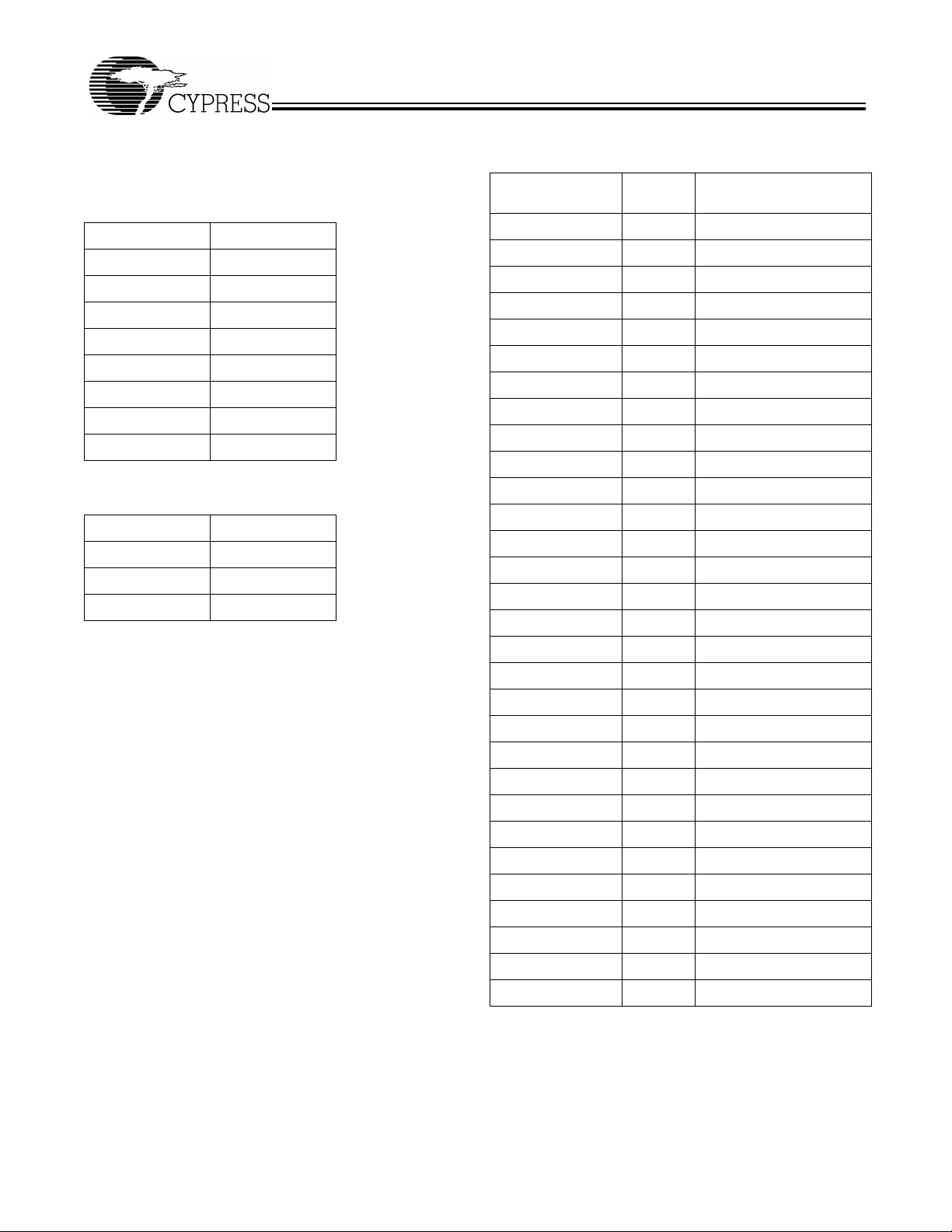
Typical DC and AC Characteristics
NORMALIZED SUPPLYCURRENT
vs. SUPPLY VOLTAGE
1.6
V
CC
A
8
A
9
A
10
V
PP
VFY
PGM
D
7
D
6
D
5
D
4
D
3
C291A-8
Figure 1. Programming Pinouts
NORMALIZED SUPPLY CURRENT
vs. AMBIENT TEMPERATURE
1.2
NC
A
5
4
A
6
3
A
2
7
A
1
8
A
9
0
10
D
11
0
5
A
A6A
321 27
4
7C291A
7C293A
1314151617
12
1
2
D
D
GND
CY7C292A/CY7C293A
7
8
9
CC
NC
V
A
A
28
26
A
25
10
V
24
PP
VFY
23
PGM
22
21
NC
20
D
7
19
D
6
18
3
5
D
D4D
NC
C291A-9
NORMALIZED ACCESSTIME
vs.SUPPLY VOLTAGE
1.2
1.4
CC
1.2
1.0
NORMALIZED I
0.8
TA=25°C
f= f
MAX
0.6
4.0 4.5 5.0 5.5 6.0
SUPPLY VOLTAGE (V)
NORMALIZED ACCESSTIME
vs.
TEMPERATURE
1.6
1.4
1.2
1.0
0.8
NORMALIZED ACCESS TIME
0.6
−
55 125
25
AMBIENT TEMPERATURE(°C)
CC
1.1
1.0
0.9
NORMALIZED I
0.8
−
55 25 125
AMBIENT TEMPERATURE (°C)
OUTPUT SOURCECURRENT
vs.
VOLTAGE
60
50
40
30
20
10
0
OUTPUT SOURCE CURRENT (mA)
0 1.0 2.0 3.0
OUTPUT VOLTAGE (V)
4.0
1.0
0.8
0.6
TA=25°C
NORMALIZED ACCESS TIME
0.4
4.0 4.5 5.0 5.5 6.0
SUPPLY VOLTAGE (V)
TYPICAL ACCESSTIME CHANGE
vs.OUTPUT LOADING
30.0
25.0
20.0
AA
15.0
10.0
DELTA t (ns)
V
=4.5V
5.0
0.0
0 200 400 600 800
T
CC
=25°C
A
CAPACITANCE (pF)
C291A-10
1000
7
Page 8

CY7C291A
CY7C292A/CY7C293A
Typical DC and AC Characteristics
OUTPUT SINK CURRENT
vs.OUT PUT
175
150
125
100
75
50
25
OUTPUT SINK CURRENT (mA)
0
0.0 1.0 2.0 3.0
Ordering Information
Speed
(ns)
I
CC
(mA) Ordering Code
VOLTAGE
=5.0V
V
CC
T
=25°C
A
OUTPUT VOLTAGE (V)
[9]
4.0
Package
Name Package Type
20 120 CY7C291A-20JC J64 28-Lead Plastic Leaded Chip Carrier Commercial
I
vs.CYCLEPERIOD
CC
1.02
1.00
CC
0.98
0.96
0.94
0.92
NORMALIZED I
0.90
0.88
025 5075
CYCLEPERIOD (ns)
VCC=5.5V
T
=25°C
A
100
Operating
Range
C291A-11
CY7C291A-20PC P13 24-Lead (300-Mil) Molded DIP
CY7C291A-20SC S13 24-Lead Molded SOIC
CY7C291A-20WC W14 24-Lead (300-Mil) Windowed CerDIP
25 60 CY7C291AL-25JC J64 28-Lead Plastic Leaded Chip Carrier Commercial
CY7C291AL-25PC P13 24-Lead (300-Mil) Molded DIP
CY7C291AL-25WC W14 24-Lead (300-Mil) Windowed CerDIP
90 CY7C291A-25JC J64 28-Lead Plastic Leaded Chip Carrier
CY7C291A-25PC P13 24-Lead (300-Mil) Molded DIP
CY7C291A-25SC S13 24-Lead Molded SOIC
CY7C291A-25WC W14 24-Lead (300-Mil) Windowed CerDIP
120 CY7C291A-25DMB D14 24-Lead (300-Mil) CerDIP Military
CY7C291A-25LMB L64 28-Square Leadless Chip Carrier
CY7C291A-25QMB Q64 28-Pin Windowed Leadless Chip Carrier
CY7C291A-25TMB T73 24-Lead Windowed Cerpack
CY7C291A-25WMB W14 24-Lead (300-Mil) Windowed CerDIP
30 120 CY7C291A-30DMB D14 24-Lead (300-Mil) CerDIP Military
CY7C291A-30LMB L64 28-Square Leadless Chip Carrier
CY7C291A-30QMB Q64 28-Pin Windowed Leadless Chip Carrier
CY7C291A-30TMB T73 24-Lead Windowed Cerpack
CY7C291A-30WMB W14 24-Lead (300-Mil) Windowed CerDIP
35 60 CY7C291AL-35JC J64 28-Lead Plastic Leaded Chip Carrier Commercial
8
Page 9

CY7C291A
Ordering Information
Speed
(ns)
Notes:
9. Most of these products are available in industrial temperature range. Contact a Cypress representative for specifications and product
I
CC
(mA) Ordering Code
CY7C291AL-35PC P13 24-Lead (300-Mil) Molded DIP
CY7C291AL-35WC W14 24-Lead (300-Mil) Windowed CerDIP
90 CY7C291A-35SC S13 24-Lead Molded SOIC Commercial
CY7C291A-35PC P13 24-Lead (300-Mil) Molded DIP
CY7C291A-35WC W14 24-Lead (300-Mil) Windowed CerDIP
120 CY7C291A-35DMB D14 24-Lead (300-Mil) CerDIP Military
CY7C291A-35LMB L64 28-Square Leadless Chip Carrier
CY7C291A-35QMB Q64 28-Pin Windowed Leadless Chip Carrier
CY7C291A-35TMB T73 24-Lead Windowed Cerpack
CY7C291A-35WMB W14 24-Lead (300-Mil) Windowed CerDIP
availability.
[9]
(Continued)
Package
Name Package Type
CY7C292A/CY7C293A
Operating
Range
9
Page 10

CY7C291A
Ordering Information
Speed
(ns)
50 60 CY7C291AL-50JC J64 28-Lead Plastic Leaded Chip Carrier Commercial
20 120 CY7C292A-20DC D12 24-Lead (600-Mil) CerDIP Commercial
I
CC
(mA) Ordering Code
CY7C291AL-50PC P13 24-Lead (300-Mil) Molded DIP
CY7C291AL-50WC W14 24-Lead (300-Mil) Windowed CerDIP
90 CY7C291A-50SC S13 24-Lead Molded SOIC Commercial
CY7C291A-50PC P13 24-Lead (300-Mil) Molded DIP
CY7C291A-50WC W14 24-Lead (300-Mil) Windowed CerDIP
90 CY7C291A-50DMB D14 24-Lead (300-Mil) CerDIP Military
CY7C291A-50LMB L64 28-Square Leadless Chip Carrier
CY7C291A-50QMB Q64 28-Pin Windowed Leadless Chip Carrier
CY7C291A-50TMB T73 24-Lead Windowed Cerpack
CY7C291A-50WMB W14 24-Lead (300-Mil) Windowed CerDIP
CY7C292A-20PC P11 24-Lead (600-Mil) Molded DIP
[9]
(Continued)
Package
Name Package Type
CY7C292A/CY7C293A
Operating
Range
25 120 CY7C292A-25DC D12 24-Lead (600-Mil) CerDIP Commercial
CY7C292A-25PC P11 24-Lead (600-Mil) Molded DIP
CY7C292A-25DMB D12 24-Lead (600-Mil) CerDIP Military
30 120 CY7C292A-30DMB D12 24-Lead (600-Mil) CerDIP Military
35 60 CY7C292AL-35PC P11 24-Lead (600-Mil) Molded DIP Commercial
90 CY7C292A-35DC D12 24-Lead (600-Mil) CerDIP Commercial
CY7C292A-35PC P11 24-Lead (600-Mil) Molded DIP
120 CY7C292A-35DMB D12 24-Lead (600-Mil) CerDIP Military
50 60 CY7C292AL-50PC P11 24-Lead (600-Mil) Molded DIP Commercial
90 CY7C292A-50DC D12 24-Lead (600-Mil) CerDIP Commercial
CY7C292A-50PC P11 24-Lead (600-Mil) Molded DIP
120 CY7C292A-50DMB D12 24-Lead (600-Mil) CerDIP Military
20 120 CY7C293A-20PC P13 24-Lead (300-Mil) Molded DIP Commercial
CY7C293A-20WC W14 24-Lead (300-Mil) Windowed CerDIP
25 120 CY7C293A-25PC P13 24-Lead (300-Mil) Molded DIP Commercial
CY7C293A-25WC W14 24-Lead (300-Mil) Windowed CerDIP
CY7C293A-25DMB D14 24-Lead (300-Mil) CerDIP Military
CY7C293A-25LMB L64 28-Square Leadless Chip Carrier
CY7C293A-25QMB Q64 28-Pin Windowed Leadless Chip Carrier
CY7C293A-25WMB W14 24-Lead (300-Mil) Windowed CerDIP
10
Page 11

CY7C291A
Ordering Information
Speed
(ns)
30 120 CY7C293A-30DMB D14 24-Lead (300-Mil) CerDIP Military
35 60 CY7C293AL-35PC P13 24-Lead (300-Mil) Molded DIP Commercial
50 60 CY7C293AL-50PC P13 24-Lead (300-Mil) Molded DIP Commercial
I
CC
(mA) Ordering Code
CY7C293A-30LMB L64 28-Square Leadless Chip Carrier
CY7C293A-30QMB Q64 28-Pin Windowed Leadless Chip Carrier
CY7C293A-30WMB W14 24-Lead (300-Mil) Windowed CerDIP
CY7C293AL-35WC W14 24-Lead (300-Mil) Windowed CerDIP
90 CY7C293A-35PC P13 24-Lead (300-Mil) Molded DIP Commercial
CY7C293A-35WC W14 24-Lead (300-Mil) Windowed CerDIP
90 CY7C293A-35DMB D14 24-Lead (300-Mil) CerDIP Military
CY7C293A-35LMB L64 28-Square Leadless Chip Carrier
CY7C293A-35QMB Q64 28-Pin Windowed Leadless Chip Carrier
CY7C293A-35WMB W14 24-Lead (300-Mil) Windowed CerDIP
[9]
(Continued)
Package
Name Package Type
CY7C292A/CY7C293A
Operating
Range
CY7C293AL-50WC W14 24-Lead (300-Mil) Windowed CerDIP
90 CY7C293A-50PC P13 24-Lead (300-Mil) Molded DIP Commercial
CY7C293A-50WC W14 24-Lead (300-Mil) Windowed CerDIP
90 CY7C293A-50DMB D14 24-Lead (300-Mil) CerDIP Military
CY7C293A-50LMB L64 28-Square Leadless Chip Carrier
CY7C293A-50QMB Q64 28-Pin Windowed Leadless Chip Carrier
CY7C293A-50WMB W14 24-Lead (300-Mil) Windowed CerDIP
11
Page 12
CY7C291A
MILITARY SPECIFICATIONS
Group A Subgroup Testing
DC Characteristics
Parameter Subgroups
V
OH
V
OL
V
IH
V
IL
I
IX
I
OZ
I
CC
[10]
I
SB
1, 2, 3
1, 2, 3
1, 2, 3
1, 2, 3
1, 2, 3
1, 2, 3
1, 2, 3
1, 2, 3
Switching Characteristics
Parameter Subgroups
t
AA
[11]
t
ACS1
[10]
t
ACS2
Notes:
10. 7C293A only.
11. 7C291A and 7C292A only.
Document #: 38-00075-G
7, 8, 9, 10, 11
7, 8, 9, 10, 11
7, 8, 9, 10, 11
CY7C292A/CY7C293A
SMD Cross Reference
SMD
Number Suffix
5962-87650 01KX CY7C291-50TMB
5962-87650 01LX CY7C291-50WMB
5962-87650 013X CY7C291-50QMB
5962-87650 03KX CY7C291-35TMB
5962-87650 03LX CY7C291-35WMB
5962-87650 033X CY7C291-35QMB
5962-88680 01LX CY7C293A-50WMB
5962-88680 01KX CY7C293A-50TMB
5962-88680 013X CY7C293A-50QMB
5962-88680 02LX CY7C293A-35WMB
5962-88680 02KX CY7C293A-35TMB
5962-88680 023X CY7C293A-35QMB
5962-88680 03LX CY7C293A-30WMB
5962-88680 03KX CY7C293A-30TMB
5962-88680 033X CY7C293A-30QMB
5962-88680 04LX CY7C293A-25WMB
5962-88680 04KX CY7C293A-25TMB
5962-88680 043X CY7C293A-25QMB
5962-88734 02JX CY7C292A-45DMB
Cypress
Number
5962-88734 02KX CY7C291A-45KMB
5962-88734 02LX CY7C291A-45DMB
5962-88734 023X CY7C291A-45LMB
5962-88734 03JX CY7C292A-35DMB
5962-88734 03KX CY7C291A-35KMB
5962-88734 03LX CY7C291A-35DMB
5962-88734 033X CY7C291A-35LMB
5962-88734 04JX CY7C292A-25DMB
5962-88734 04KX CY7C291A-25KMB
5962-88734 04LX CY7C291A-25DMB
5962-88734 043X CY7C291A-25LMB
12
Page 13

CY7C291A
28-Square LeadlessChipCarrier L64
MIL-STD-1835 C-4
Package Diagrams
24-Lead (600-Mil) CerDIP D12
MIL-STD-1835 D-3 Config.A
CY7C292A/CY7C293A
24-Lead (300-Mil) CerDIP D14
MIL-STD-1835 D-9Config.A
13
Page 14

CY7C291A
Package Diagrams (Continued)
24-Lead (600-Mil) Molded DIP P11
24-Lead (300-Mil) Molded DIP P13/P13A
CY7C292A/CY7C293A
14
Page 15

CY7C291A
Package Diagrams
28-Pin Windowed LeadlessChipCarrier Q64
MIL-STD-1835 C-4
(Continued)
CY7C292A/CY7C293A
24-Lead (300-Mil) Molded SOIC S13
© Cypress Semiconductor Corporation, 1993. The information contained herein is subject to change without notice. Cypress Semiconductor Corporation assumes no responsibility for the use
of any circuitry other than circui try embodied in a Cypress S emiconductor p roduct. Nor does it conv ey or imply an y license under pa tent or other rights. Cypre ss Semiconductor doe s not authorize
its products for use as critical components in life-support systems where a malfunction or failure may reasonably be expected to result in significant injury to the user. The inclusion of Cypress
Semiconductor products in life-support systems application implies that the manufacturer assumes all risk of such use and in doing so indemnifies Cypress Semiconductor against all charges.
Page 16

CY7C291A
Package Diagrams (Continued)
24-Lead Windowed Cerpack T73
CY7C292A/CY7C293A
24-Lead (300-Mil) WindowedCerDIP W14
MIL-STD-1835 D-9 Config.A
16
 Loading...