

77
查询CY7C277-30JC供应商
CY7C277
32K x 8 Reprogrammable Registered PROM
Features
• Windowed for reprogrammability
• CMOS for optimum speed/power
• High speed
—30-ns address set-up
—15-ns clock to output
• Low power
—60 mW (commercial)
—715 mW (military)
• Programmable address latch enable input
• Programmable synchronous or asynchronous output
enable
• On-chip edge-triggered output registers
• EPROM technology, 100% programmable
• Slim 300-mil, 28-pin plastic or hermetic DIP
• 5V ±10% V
, commercial and military
CC
• TTL-compatible I/O
• Direct replacement for bipolar PROMs
• Capable of wi thstanding greater than 2001V static dis-
charge
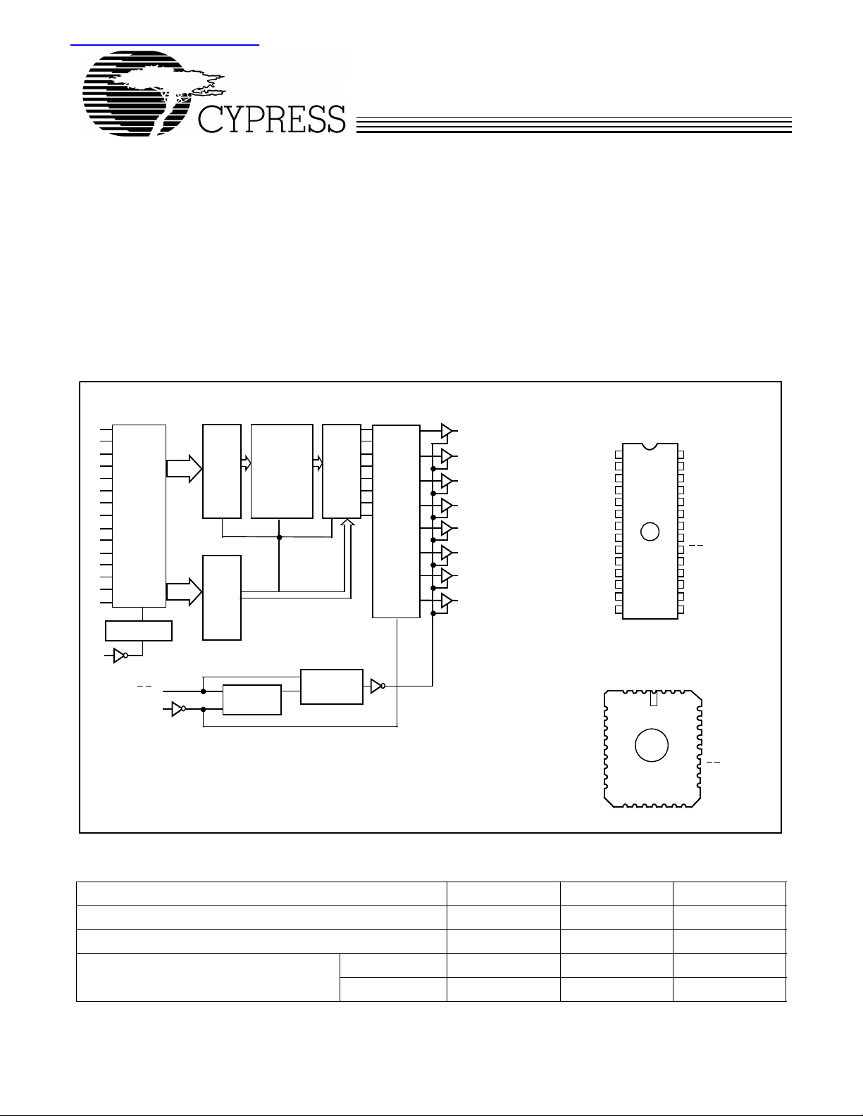
Logic Block Diagram Pin Configurations
A
A
A
A
A
14
13
12
11
10
A
9
A
8
A
7
A
6
A
5
A
4
A
3
A
2
A
1
A
0
ALE
15-BIT
ADDRESS
TRANSPARENT/
LATCH
ALE
PROGRAMMABLE
CP/ALE
OPTIONS
E/E
S
CP
X
ADDRESS
Y
ADDRESS
ROW
DECODER
256
1OF
COLUMN
DECODER
32
1OF
D
C
256 x 1024
PROGRAMMABLE
ARRAY
Q
8-BIT
1 OF 128
MUX
PROGRAMMABLE
MULTIPLEXER
8-BIT
EDGE-
TRIGGERED
REGISTER
CP
O
7
O
6
O
5
O
4
O
3
O
2
O
1
O
0
DIP/Flatpack
Top View
1
28
2
27
3
26
4
25
5
24
6
23
22
7
21
8
9
20
10
19
11
18
12
17
13
16
14
15
GND
A
9
A
8
A
7
A
6
A
5
A
4
A
3
A
2
A
1
A
0
O
0
O
1
O
2
LCC/PLCC (Opaque Only)
Top V iew
CC
V
A9A10A
NC
31
32
1
181920
3
O
O
NC
GND
11
30
29
28
27
26
25
24
23
22
21
4
NC
8
7
A
A
4
6
5
4
3
2
1
0
0
5
6
7
8
9
10
11
12
13
14151617
32
1
O2O
A
A
A
A
A
A
A
O
V
A
A
A
A
A
ALE
CP
E
O
O
O
O
O
5
O
CC
10
11
12
13
14
/E
S
7
6
5
4
3
A
12
A
13
A
14
NC
ALE
CP
E/E
S
O
7
O
6
Selection Guide
7C277-30 7C277-40 7C277-50
Minimum Address Set-Up Time (ns) 30 40 50
Maximum Clock to Output (ns) 15 20 25
Maximum Operat ing
Current (mA)
Cypress Semiconductor Corporation • 3901 North First Street • San Jose • CA 95134 • 408-943-2600
Document #: 38-04006 Rev. ** Revised March 4, 2002
Com’l 120 120 120
Mil 130 130
CY7C277
Functional Description
The user may define the polarity of the ALE signal, with the
default being active HIGH.
The CY7C277 is a hi gh-performance 32 K word by 8-bit CMOS
PROMs. It is packaged in the slim 28-pin 300-mil package.
Maximum Ratings
The ceramic package may be equipped with an erasure window; when exposed to UV l igh t, the PRO M is erased and can
then be reprogrammed. The memory cells utilize proven
EPROM floating-gate technology and byte-wide algorithms.
The CY7C277 offers the advantages of low power, superior
performance, and high programming yield. The EPROM cell
requires only 12.5V for the supervoltage and low current requirements allow for gang programming. The EPROM cells
allow for each memory location to be 100% tested, as each
location is written into, era sed, and repeated ly exercis ed prior
to encapsulation. Each PROM is also tested for AC performance to guarantee that the product will meet DC and AC
specification limits after customer programming.
On the 7C277, the outputs are pipelined through a master-slave register. On the rising edge of CP, data is loaded into
the 8-bit edge triggered output register. The E
/ES input provides a programmable bit to select between asynchronous
and synchronous oper ation. The default cond ition is asynchronous. When the as ynchronou s mod e is s elect ed, the E
/ES pin
operates as an asynchronous output enable. If the synchronous mode is selected, the E
/ES pin is sampled on the rising
edge of CP to ena ble and disa ble the outpu ts. The 7C2 77 also
provides a programmable bit to enable the Address Latch input. If this bit is not pr ogrammed, the device w ill ignore the ALE
pin and the address will enter the device asynchron ously . If the
ALE function is selected, the address enters the PROM while
the ALE pin is active, and is captured when ALE is deasserted.
Electrical Characteristics Over the Operating Range
(Above which the usef ul life ma y be impaire d. For user g uidelines, not tested.)
Storage Temperature ....................................−65°C to +150°C
Ambient Temperature with
Power Applied.................................................−55°C to +125°C
Supply Voltage to Ground Potential.................−0.5V to +7.0V
(Pin 24 to Pin 12)
DC Voltage Applied to Outputs
in High Z State.....................................................−0.5V to +7.0V
DC Input Voltage.................................................−3.0V to +7.0V
DC Program Voltage (Pins 7, 18, 20)...........................13.0V
UV Erasure ...................................................7258 Wsec/cm
Static Discharge Voltage ...........................................>2001V
(per MIL-STD-883, Method 3015)
Latch-Up Current.....................................................>200 mA
Operating Range
Range Ambient Temperature V
Commercial 0°C to +70°C 5V ±10%
[2]
[1]
−40°C to +85°C 5V ±10%
−55°C to +125°C 5V ±10%
Industrial
Military
[3, 4]
7C277-30 7C277-40, 50
Parameter
V
OH
V
OL
V
IH
V
IL
I
IX
V
CD
I
OZ
I
OS
I
CC
V
PP
I
PP
V
IHP
V
ILP
Notes:
1. Contact a Cypress representative for industrial temperature range specifications.
2. T
is the “instant on ” case temperatu re.
A
3. See the last page of this specification for Gro up A subgro up testing information.
4. See “Introduction to CMOS PROMs” in this Book for general information on testing.
5. For devices using the synchronous enable, the device must be clocked after applying these voltages to perform this measurement.
6. For test purposes, not more than one output at a time should be shorted. Short circuit test duration should not exceed 30 seconds.
Output HIGH Voltage VCC = Min., IOH = − 2.0 mA 2.4 2.4 V
Output LOW Voltage VCC = Min., IOL = 8.0 mA 0.4 0.4 V
Input HIGH Level Guaranteed Input Logical HIGH
Input LOW Level Guaranteed Input Logical LOW
Input Leakage Current GND < VIN < V
Input Clamp Diode Voltage Note 4
Output Leakage Current 0 < V
Output Short Circuit Current VCC = Max., V
Power Supply Current VCC = Max., CS > V
Programming Supply Voltage 12 13 12 13 V
Programming Supply Current 50 50 mA
Input HIGH Programming Voltage 3.0 3.0 V
Input LOW Programming Voltage 0.4 0.4 V
Description Test Conditions Min. Max. Min. Max. Unit
Voltage for All Inputs
2.0 V
CC
0.8 0.8 V
Voltage for All Inputs
−10 +10 −10 +10 µA
[5]
−40 +40 −40 +40 µA
−20 −90 −20 −90 mA
I
OUT
CC
< VCC, Output Disabled
OUT
= 0.0V
OUT
= 0 mA
[6]
Commercial 120 120 mA
IH
Military 130
2.0 V
CC
2
CC
V
Document #: 38-04006 Rev. ** Page 2 of 13
CY7C277
Capacitance
[4]
Parameter Description Test Conditions Max. Unit
C
IN
C
OUT
AC Test Loads and Wavefor ms
R1 500Ω
5V
OUTPUT
30 pF
INCLUDING
JIG AND
SCOPE
(658
(a) NormalLoad
Equivalent to: THÉ VENIN EQUIVALENT
OUTPUT 2.0V
CY7C277 Switching Characteristics Over the Operating Range
Input Capacitance TA = 25°C, f = 1 MHz,
= 5.0V
V
R1 500
Load
Ω
CC
R2
333
3.0V
Ω
GND
<5ns
OUTPUT 1.9V
250Ω
Military
[3, 4]
Output Capacitance 10 pF
[4]
Ω MIL)
R2
333
Ω
Ω MIL) (403Ω MIL)
(403
5V
OUTPUT
INCLUDING
JIG AND
SCOPE
(658Ω MIL)
5pF
(b) HighZ
Ω
200
Commercial
10 pF
ALL INPUT PULSES
90%
10%
90%
10%
<5ns
7C277-30 7C277-40 7C277-50
Parameter Description Min. Max. Min. Max. Min. Max. Unit
t
AL
t
LA
t
LL
t
SA
t
HA
t
SES
t
HES
t
CO
t
PWC
[7]
t
LZC
t
HZC
[8]
t
LZE
[8]
t
HZE
Notes:
7. Applies only when the synchronous (E
8. Applies only when the asynchronous (E
Address Set-Up to ALE Inactive 5 10 10 ns
Address Hold from ALE Inactive 10 10 15 ns
ALE Pulse Width 10 10 15 ns
Address Set-Up to Clock HIGH 30 40 50 ns
Address Hold from Clock HIGH 0 0 0 ns
ES Set-Up to Clock HIGH 12 15 15 ns
ES Hold from Clock HIGH 5 10 10 ns
Clock HIGH to Output Valid 15 20 25 ns
Clock Pulse Width 15 20 20 ns
Output Valid from Clock HIGH 15 20 30 ns
Output High Z from Clock HIGH 15 20 30 ns
Output Valid from E LOW 15 20 30 ns
Output High Z from E HIGH 15 20 30 ns
) function is used.
S
) function is us ed.
Document #: 38-04006 Rev. ** Page 3 of 13
Architecture Configuration Bits
Architecture Bit Architecture Verify D7 - D
ALE D
ALEP D
E/E
S
D
0 = DEFAULT Input Transparent
1
1 = PGMED Input Latched
0 = DEFAULT ALE = Active HIGH
2
1 = PGMED ALE = Active LOW
0 = DEFAULT Asynchronous Output Enable (E)
0
1 = PGMED Synchronous Output Enable (ES)
CY7C277
0
Function
Bit Map
Programmer Address
(Hex.) RAM Data
0000
.
.
.
7FFF
8000
Timing Diagram (Input Latched)
A0-A
14
t
SES
t
HZC
t
LA
ALE
(SYNCH)
O
-O
0
E
CP
t
AL
t
LL
S
7
t
t
CO
HES
Data
.
.
.
Data
Control Byte
[9]
t
PWC
t
HES
t
PWC
HIGHZ
Architecture Byte (8000
)
D7 D0
C
7C6C5C4 C3
t
SES
t
LZC
C2 C1 C
t
SA
t
HZE
0
t
HA
HIGHZ
t
LZE
E
(ASYNCH)
S
Timing Diagram (Input Transparent)
A0-A
14
t
SA
E
S
(SYNCH)
CP
t
HES
t
CO
t
SES
t
HZC
t
PWC
t
HES
t
PWC
t
SES
t
LZC
HIGHZ
O
-O
0
7
t
HZE
E
(ASYNCH)
Note:
S
9. ALE is shown with positive polarity.
Document #: 38-04006 Rev. ** Page 4 of 13
t
HA
HIGHZ
t
LZE

CY7C277
Programming Information
Programming support is available from Cypress as well as
from a number of third-party software vendors. For detailed
Table 1. Mode Selection
Read or Output Disable A14–A
Mode Other A14–A
Read A14–A
Output Disable A14–A
Program A14–A
Program Verify A14–A
Program Inhibit A14–A
Blank Check A14–A
Note:
10. X = “don’t care” but not to exceed V
±5%.
CC
DIP LCC/PLCC (Opaque Only)
Top V iew Top View
1
A
9
2
A
8
3
A
7
4
A
6
5
A
5
6
A
4
A
7
3
A
8
2
A
9
1
A
10
0
11
D
0
12
D
1
13
D
2
GND
14
0
0
0
0
0
0
0
0
28
V
CC
27
A
10
26
A
11
25
A
12
24
A
13
23
A
14
22
V
PP
21
PGM
20
VFY
19
D
7
D
18
6
D
17
5
D
16
4
D
15
3
programming inform ation, in cludi ng a list ing of sof tware packages, please see the PRO M Programming Information located
at the end of this s ection . Program ming algorit hms can be o btained from any Cypress representative.
NC
1
GND
CC
V
31
32
181920
3
D
NC
[10]
PP
V
IL
V
PP
V
PP
V
PP
V
PP
11
30
A
12
29
A
13
28
A
14
27
26
NC
25
V
PP
PGM
24
VFY
23
D
22
7
21
D
6
4
5
D
D
Pin Function
E, E
S
CP ALE O7–O
VFY PGM V
V
IL
V
IH
V
IHP
V
ILP
V
IHP
V
ILP
A
6
A
5
A
4
A
3
A
2
A
1
A
0
NC
D
0
V
IH
X X High Z
V
ILP
V
IHP/VILP
V
IHP
V
IHP/VILP
7
A
A8A9A10A
4
32
5
6
7
8
9
10
11
12
13
14151617
1
D2D
D7–D
O7–O
D7–D
O7–O
High Z
O7–O
0
0
0
0
0
0
Figure 1. Programming Pinouts
Document #: 38-04006 Rev. ** Page 5 of 13

Typical DC and AC Characteristics
CY7C277
NORMALIZED SUPPLY CURRENT
vs. SUPPLY VOLTAGE
1.6
1.4
CC
1.2
1.0
NORMALIZED I
=25°C
T
0.8
A
f= f
MAX
0.6
4.0 4.5 5.0 5.5 6.0
SUPPLYVOLTAGE (V )
NORMALIZED SET-UP TIME
vs. TEMPERATURE
1.6
1.4
1.2
1.0
0.8
NORMALIZED SET-UP TIME
0.6
−55 125
25
AMBIENT TEMPERATURE (
°C)
NORMALIZED SUPPLY CURRENT
vs. AMBIENT TEMPERATURE
1.2
1.1
CC
1.0
0.9
NORMALIZED I
0.8
−55 25 125
AMBIENTTEMPERATURE (
OUTPUT SOURCE CURRENT
vs. VOLTAGE
60
50
40
30
20
10
0
OUTPUT SOURCE CURRENT (mA)
0 1.0 2.0 3.0
OUTPUT VOLTAGE (V)
°C)
4.0
NORMALIZED ACCESS TIME
vs. SUPPLY VOLTAGE
1.2
1.0
0.8
0.6
T
NORMALIZED ACCESS TIME
0.4
A
4.0 4.5 5.0 5.5 6.0
SUPPLYVOLTAGE (V)
TYPICAL ACCESS TIME CHANGE
vs. OUTPUT LOADING
30.0
25.0
20.0
AA
15.0
10.0
DELTA t (ns)
T
=25°C
5.0
0.0
0 200 400 600 800
A
V
CC
CAPACITANCE (pF)
=25°C
=4.5V
1000
OUTPUT SINK CURRENT
vs. OUTPUT VOLTAGE
175
150
125
100
75
50
25
OUTPUT SINK CURRENT (mA)
VCC=5.0V
=25°C
T
A
0
0.0 1.0 2.0 3.0
4.0
OUTPUT VOLTAGE (V)
C277-12
Document #: 38-04006 Rev. ** Page 6 of 13

CY7C277
Ordering Information
Speed
(ns) Ordering Code
[11]
Package
Name Package Type
Operating
30 CY7C277-30JC J65 32-Lead Plastic Leaded Chip Carrier Commercial
CY7C277-30PC P21 28-Lead (300-Mil) Molded DIP
CY7C277-30WC W22 28-Lead (300-Mil) Windowed CerDIP
40 CY7C277-40JC J65 32-Lead Plastic Leaded Chip Carrier Commercial
CY7C277-40PC P21 28-Lead (300-Mil) Molded DIP
CY7C277-40WC W22 28-Lead (300-Mil) Windowed CerDIP
CY7C277-40DMB D22 28-Lead (300-Mil) CerDIP Military
CY7C277-40KMB K74 28-Lead Rectangular Cerpack
CY7C277-40LMB L55 32-Pin Rectangular Leadless Chip Carrier
CY7C277-40QMB Q55 32-Pin Windo wed Rectangular Le adless Chip Carrier
CY7C277-40TMB T74 28-Lead Windowed C erpack
CY7C277-40WMB W22 28-Lead (300-Mil) Windowed CerDIP
50 CY7C277-50JC J65 32-Lead Plastic Leaded Chip Carrier Commercial
CY7C277-50PC P21 28-Lead (300-Mil) Molded DIP
CY7C277-50WC W22 28-Lead (300-Mil) Windowed CerDIP
CY7C277-50DMB D22 28-Lead (300-Mil) CerDIP Military
Range
CY7C277-50KMB K74 28-Lead Rectangular Cerpack
CY7C277-50LMB L55 32-Pin Rectangular Leadless Chip Carrier
CY7C277-50QMB Q55 32-Pin Windo wed Rectangular Le adless Chip Carrier
CY7C277-50TMB T74 28-Lead Windowed C erpack
CY7C277-50WMB W22 28-Lead (300-Mil) Windowed CerDIP
Note:
11. Most of the above products are available in industrial temperature range. Contact a Cypress representative for specifications and product
availability.
MILITARY SPECIFICATIONS
Group A Subgroup Testing
DC Characteristics
Parameter Subgroups
V
OH
V
OL
V
IH
V
IL
I
IX
I
OZ
I
CC
1, 2, 3
1, 2, 3
1, 2, 3
1, 2, 3
1, 2, 3
1, 2, 3
1, 2, 3
Switching Characteristics
Parameter Subgroups
t
t
t
SA
HA
CO
7, 8, 9, 10, 11
7, 8, 9, 10, 11
7, 8, 9, 10, 11
Document #: 38-04006 Rev. ** Page 7 of 13

Package Diagrams
CY7C277
28-Lead (300-Mil) CerDIP D22
MIL-STD-1835 D-15 Config. A
32-Lead Plastic Leaded Chip Carrier J65
51-80032
51-85002-B
Document #: 38-04006 Rev. ** Page 8 of 13

Package Diagrams (continued)
CY7C277
28-Lead Rectangular Cerpack K74
MIL-STD-1835 F-11 Config. A
51-80061
Document #: 38-04006 Rev. ** Page 9 of 13

Package Diagrams (continued)
CY7C277
32-Pin Rectangular Leadless Chip Carrier L55
MIL-STD-1835 C-12
28-Lead (300-Mil) Molded DIP P21
51-80068
51-85014-B
Document #: 38-04006 Rev. ** Page 10 of 13

Package Diagrams (continued)
CY7C277
32-Pin Windowed Rectangular Leadless Chip Carrier Q55
MIL-STD-1835 C-12
51-80103-*A
Document #: 38-04006 Rev. ** P age 11 of 13

ng so indemnifies Cypress Semiconductor against all charges.
Package Diagrams (continued)
CY7C277
28-Lead Windowed Cerpack T74
28-Lead
(300-Mil)
MIL-STD-1835 D- 15 Conf ig. A
Windowed CerDIP W22
Document #: 38-04006 Rev. ** Page 12 of 13
© Cypress Semiconductor Corporation, 2002. The information contained herein is subject to change without notice. Cypress Semiconductor Corporation assumes no responsibility for the use
of any circuitry other than circuitry embodied in a Cypress Semiconductor product. No r does it convey or imply any license under patent or other rights. Cypress Semiconductor does not autho rize
its products for use as critical components in life-support systems where a malfunction or failure may reasonably be expected to result in significant injury to the user. The inclusion of Cypress
Semiconductor products in life-support systems application implies that the manufacturer assume s all risk of such use and in doi
51-80087

Document Title: CY7C277 32K x 8 Programmable Registered PROM
Document Number: 38-04006
REV. ECN NO.
** 113862 3/8/02 DSG Change from Spec number: 38-00085 to 38-04006
Issue
Date
Orig. of
Change Description of Change
CY7C277
Document #: 38-04006 Rev. ** Page 13 of 13
 Loading...