

Page 1
50
WWW.100Y.COM.TW WWW.100Y.COM.TW WWW.100Y.COM.TW
WWW.100Y.COM.TW WWW.100Y.COM.TW WWW.100Y.COM.TW
WWW.100Y.COM.TW WWW.100Y.COM.TW WWW.100Y.COM.TW
WWW.100Y.COM.TW WWW.100Y.COM.TW WWW.100Y.COM.TW
WWW.100Y.COM.TW WWW.100Y.COM.TW WWW.100Y.COM.TW
WWW.100Y.COM.TW WWW.100Y.COM.TW WWW.100Y.COM.TW
WWW.100Y.COM.TW WWW.100Y.COM.TW WWW.100Y.COM.TW
WWW.100Y.COM.TW WWW.100Y.COM.TW WWW.100Y.COM.TW
WWW.100Y.COM.TW WWW.100Y.COM.TW WWW.100Y.COM.TW
WWW.100Y.COM.TW WWW.100Y.COM.TW WWW.100Y.COM.TW
WWW.100Y.COM.TW WWW.100Y.COM.TW WWW.100Y.COM.TW
WWW.100Y.COM.TW WWW.100Y.COM.TW WWW.100Y.COM.TW
WWW.100Y.COM.TW WWW.100Y.COM.TW WWW.100Y.COM.TW
WWW.100Y.COM.TW WWW.100Y.COM.TW WWW.100Y.COM.TW
WWW.100Y.COM.TW WWW.100Y.COM.TW WWW.100Y.COM.TW
WWW.100Y.COM.TW WWW.100Y.COM.TW WWW.100Y.COM.TW
WWW.100Y.COM.TW WWW.100Y.COM.TW WWW.100Y.COM.TW
WWW.100Y.COM.TW WWW.100Y.COM.TW WWW.100Y.COM.TW
WWW.100Y.COM.TW WWW.100Y.COM.TW WWW.100Y.COM.TW
WWW.100Y.COM.TW WWW.100Y.COM.TW WWW.100Y.COM.TW
WWW.100Y.COM.TW WWW.100Y.COM.TW WWW.100Y.COM.TW
WWW.100Y.COM.TW WWW.100Y.COM.TW WWW.100Y.COM.TW
WWW.100Y.COM.TW WWW.100Y.COM.TW WWW.100Y.COM.TW
WWW.100Y.COM.TW WWW.100Y.COM.TW WWW.100Y.COM.TW
WWW.100Y.COM.TW WWW.100Y.COM.TW WWW.100Y.COM.TW
WWW.100Y.COM.TW WWW.100Y.COM.TW WWW.100Y.COM.TW
WWW.100Y.COM.TW WWW.100Y.COM.TW WWW.100Y.COM.TW
WWW.100Y.COM.TW WWW.100Y.COM.TW WWW.100Y.COM.TW
WWW.100Y.COM.TW WWW.100Y.COM.TW WWW.100Y.COM.TW
WWW.100Y.COM.TW WWW.100Y.COM.TW WWW.100Y.COM.TW
WWW.100Y.COM.TW WWW.100Y.COM.TW WWW.100Y.COM.TW
WWW.100Y.COM.TW WWW.100Y.COM.TW WWW.100Y.COM.TW
WWW.100Y.COM.TW WWW.100Y.COM.TW WWW.100Y.COM.TW
WWW.100Y.COM.TW WWW.100Y.COM.TW WWW.100Y.COM.TW
CY7C150
Features
• Memory reset function
• 1024 x 4 static RA M for control store in high-spee d computers
• CMOS for optimum speed/power
• High speed
—10 ns (commercial)
—12 ns (military)
• Low power
—495 mW (co mmercial)
—550 mW (military)
• Separate inputs and outputs
• 5-volt power supply ±10% tolerance in both commercial
and military
• Capable of withstanding greater than 2001V static dis-
charge
• TTL-compatible inputs and outputs
Functional Description
The CY7C150 is a high-performance CMOS static RAM designed for use in cache memory, high-speed graphics, and
data-acquisition applications. The CY 7C150 has a memory reset feature that allows the entire memory to be reset in two
memory cycles.
Separate I/O paths eliminates the need to multiplex data in
and data out, pro viding for simpl er board layout and faster system performance. Output s are three-stated d uring write, reset,
deselect, or when output enable (OE
for easy memory expansion.
Reset is initiat ed by sele cting the device (CS
ing the reset (RS
) input LOW. Within two memory cycles all
bits are internally cleared to zero. Since chip select must be
LOW for the device to be reset, a global reset signal can be
employed, with onl y selected dev ices being cle ared at any given time.
Writing to the device is accomplished when the chip select
) and write enable (W E) inpu ts are both L OW. Data o n the
(CS
four data inputs (D0−D3) is written into the memory location
specified on the address pins (A
Reading the device is accomplishe d by taking chip sele ct (CS)
and output enable (OE
HIGH. Under these conditions, the contents of the memory
location specified on the address pins will appear on the four
output pins (O
through O3).
0
The output pins remain in high-impedance state when chip
enable (CE
(WE
) or output enable (OE) is HIGH, or write enable
) or reset (RS) is LOW.
A die coat is used to insure alpha immunity.
1Kx4 Static RAM
) LOW while write enable (WE) re mains
) is held HIGH, allowing
= LOW) and tak-
through A9).
0
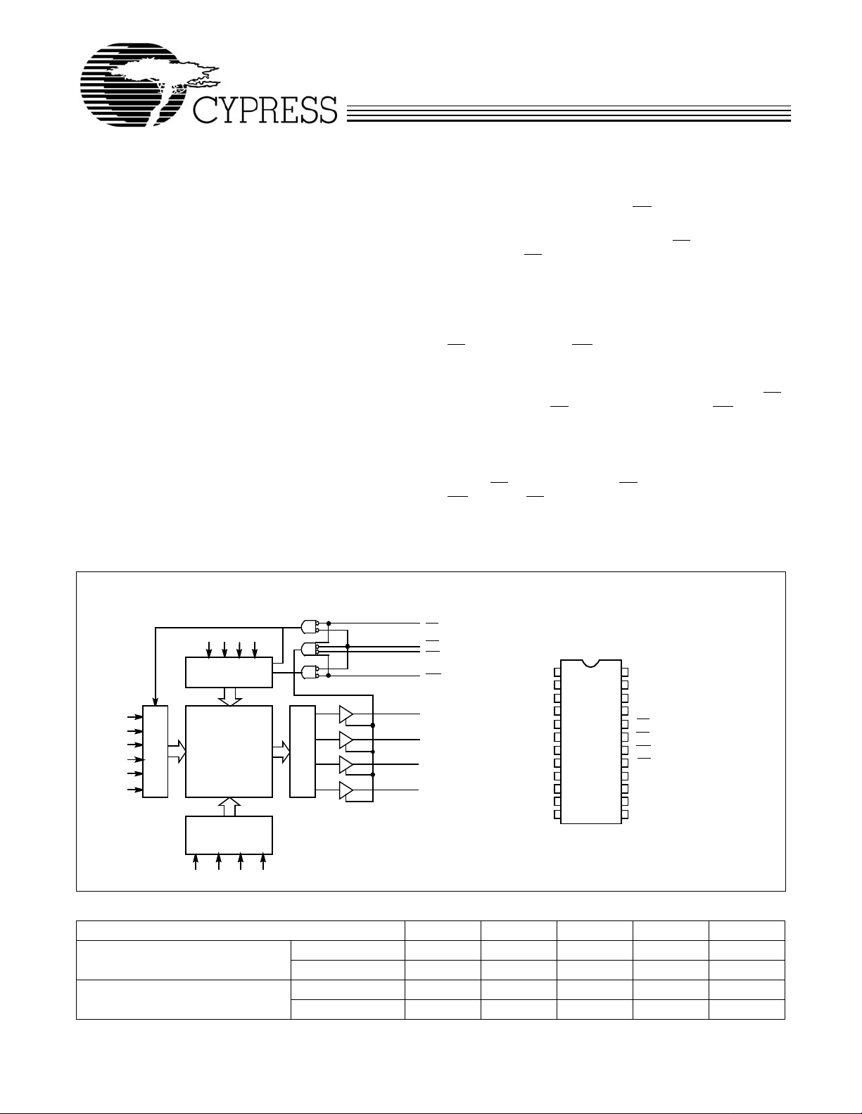
Logic Block Diagram
A
0
A
1
A
2
A
3
A
4
A
5
D0D1D2D
DATAINPUT
CONTROL
3
RS
CS
OE
WE
C150–1
O
0
O
1
O
2
O
3
ROW DECODER
64x64
ARRA
Y
SENSE AMPS
COLUMN
COLUMNDECODER
DECODER
A6A7A
A
8
9
PinConfiguration
DIP/SOIC
Top View
A
1
A
A
A
A
A
A
D
D
O
O
GND
3
2
4
3
5
4
6
5
7
8
6
7
9
8
0
9
1
10
0
11
1
12
7C150
24
23
22
21
20
19
18
17
16
15
14
13
C150-2
V
A
A
A
RS
CS
WE
OE
D
D
O
O
CC
2
1
0
3
2
3
2
Selection Guide
Maximum Access Time (ns) Commercial 10 12 15 25
Maximum Operating Current (mA) Commercial 90 90 90 90 90
7C150−10 7C150−12 7C150−15 7C150−25 7C150−35
Military 12 15 25 35
Military 100 100 100 100
Cypress Semiconductor Corporation • 3901 North First Street • San Jose • CA 95134 • 408-943-2600
Document #: 38-05024 Rev. ** Revised August 24, 2001
Page 2
WWW.100Y.COM.TW WWW.100Y.COM.TW WWW.100Y.COM.TW
WWW.100Y.COM.TW WWW.100Y.COM.TW WWW.100Y.COM.TW
WWW.100Y.COM.TW WWW.100Y.COM.TW WWW.100Y.COM.TW
WWW.100Y.COM.TW WWW.100Y.COM.TW WWW.100Y.COM.TW
WWW.100Y.COM.TW WWW.100Y.COM.TW WWW.100Y.COM.TW
WWW.100Y.COM.TW WWW.100Y.COM.TW WWW.100Y.COM.TW
WWW.100Y.COM.TW WWW.100Y.COM.TW WWW.100Y.COM.TW
WWW.100Y.COM.TW WWW.100Y.COM.TW WWW.100Y.COM.TW
WWW.100Y.COM.TW WWW.100Y.COM.TW WWW.100Y.COM.TW
WWW.100Y.COM.TW WWW.100Y.COM.TW WWW.100Y.COM.TW
WWW.100Y.COM.TW WWW.100Y.COM.TW WWW.100Y.COM.TW
WWW.100Y.COM.TW WWW.100Y.COM.TW WWW.100Y.COM.TW
WWW.100Y.COM.TW WWW.100Y.COM.TW WWW.100Y.COM.TW
WWW.100Y.COM.TW WWW.100Y.COM.TW WWW.100Y.COM.TW
WWW.100Y.COM.TW WWW.100Y.COM.TW WWW.100Y.COM.TW
WWW.100Y.COM.TW WWW.100Y.COM.TW WWW.100Y.COM.TW
WWW.100Y.COM.TW WWW.100Y.COM.TW WWW.100Y.COM.TW
WWW.100Y.COM.TW WWW.100Y.COM.TW WWW.100Y.COM.TW
WWW.100Y.COM.TW WWW.100Y.COM.TW WWW.100Y.COM.TW
WWW.100Y.COM.TW WWW.100Y.COM.TW WWW.100Y.COM.TW
WWW.100Y.COM.TW WWW.100Y.COM.TW WWW.100Y.COM.TW
WWW.100Y.COM.TW WWW.100Y.COM.TW WWW.100Y.COM.TW
WWW.100Y.COM.TW WWW.100Y.COM.TW WWW.100Y.COM.TW
WWW.100Y.COM.TW WWW.100Y.COM.TW WWW.100Y.COM.TW
WWW.100Y.COM.TW WWW.100Y.COM.TW WWW.100Y.COM.TW
WWW.100Y.COM.TW WWW.100Y.COM.TW WWW.100Y.COM.TW
WWW.100Y.COM.TW WWW.100Y.COM.TW WWW.100Y.COM.TW
WWW.100Y.COM.TW WWW.100Y.COM.TW WWW.100Y.COM.TW
WWW.100Y.COM.TW WWW.100Y.COM.TW WWW.100Y.COM.TW
WWW.100Y.COM.TW WWW.100Y.COM.TW WWW.100Y.COM.TW
WWW.100Y.COM.TW WWW.100Y.COM.TW WWW.100Y.COM.TW
WWW.100Y.COM.TW WWW.100Y.COM.TW WWW.100Y.COM.TW
WWW.100Y.COM.TW WWW.100Y.COM.TW WWW.100Y.COM.TW
WWW.100Y.COM.TW WWW.100Y.COM.TW WWW.100Y.COM.TW
CY7C150
Maximum Ratings
(Above which the useful life may be im pai red. For user guidelines, not tested.)
Storage Temperature ......................................−65°C to+150°C
Ambient Temperature with
Power Applied...................................................−55°C to+125°C
Supply Voltage to Ground Potential
(Pin 24 to Pin 12)..................................................−0.5V to+7.0V
DC Voltage Applied to Outputs
in High Z State......................................................−0.5V to+7.0V
DC Input Voltage.................................................−3.0V to +7.0V
Output Current into Outputs (LOW).............................20 mA
Electrical Characteristics Ov er the Op erat ing Range
Static Discharge Voltage.......................................... >2001V
(per MIL-STD-883, Method 3015)
Latch-Up Current.................................................... >200 mA
Operating Range
Range
Commercial 0°C to +70°C 5V ± 10%
[1]
Military
Note:
1. T
is the “instant on” case temperature.
A
[2]
Ambient
Temperature V
−55°C to +125°C 5V ± 10%
Parameter Description Test Conditions
V
OH
V
OL
V
IH
V
I
IX
I
OZ
I
OS
I
CC
Notes:
2. See the last page of this specification for Group A sub gro up test ing in for ma tion .
3. Not more than 1 output should be shorted at a time. Duration of the short circuit should not exceed 30 seconds.
IL
Output HIGH Voltage VCC = Min., I
Output LOW Current VCC = Min., I
Input HIGH Level 2.0 V
Input LOW Level −3.0 0.8 V
Input Load Current GND < VI < V
Output Current (High Z) VOL < V
Output Short Circuit Current
VCC Operating Supply Current V
Output Disabled
[3]
VCC = Max., V
I
CC
OUT
OUT
= Max.,
= 0 mA
= − 0.4 mA 2.4 V
OH
= 12 mA 0.4 V
OL
CC
< VOH,
= GND −300 mA
OUT
Commercial 90 mA
Military 100 mA
Capacitance
Parameter Description Test Conditions Max. Unit
C
IN
C
OUT
Note:
4. Tested initially and after any design or process changes that may affect these parameters.
[4]
Input Capacitance TA = 25°C, f = 1 MHz,
Output Capacitance 10 pF
V
= 5.0V
CC
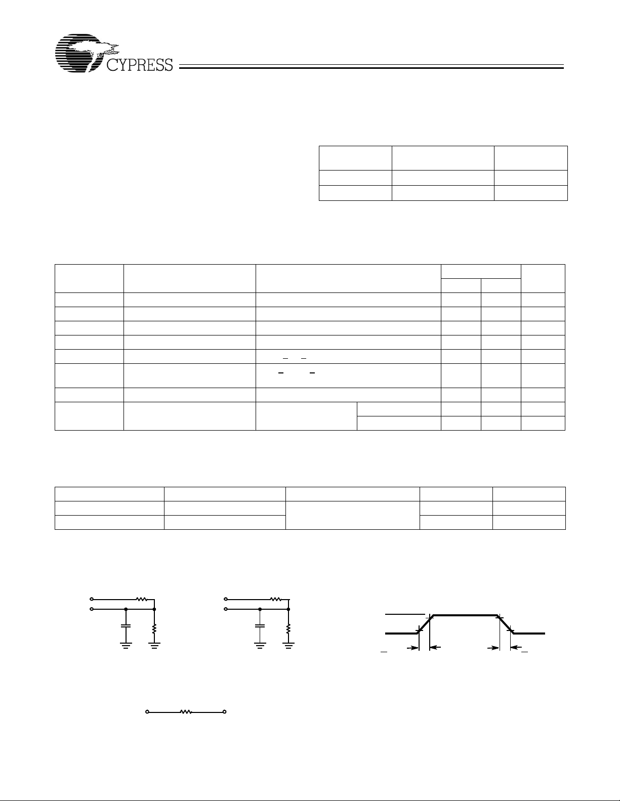
AC Test Loads and Waveforms
CC
7C150
UnitMin. Max.
CC
−10 +10 µA
−50 +50 µA
10 pF
V
5V
OUTPUT
INCLUDING
30 pF
JIG AND
SCOPE
R1329
(a) (b)
Ω
R2
202
Ω
5V
OUTPUT
5 pF
INCLUDING
JIG AND
SCOPE
R1329
Ω
R2
202
C150–3
3.0V
Ω
GND
10%
<3ns <3ns
ALL INPUT PULSES
90%
90%
10%
C150–4
Equivalent to: THÉ VENIN EQUIVALENT
Ω
OUTPUT 1.9V
Document #: 38-05024 Rev. ** Page 2 of 11
125
Page 3
WWW.100Y.COM.TW WWW.100Y.COM.TW WWW.100Y.COM.TW
WWW.100Y.COM.TW WWW.100Y.COM.TW WWW.100Y.COM.TW
WWW.100Y.COM.TW WWW.100Y.COM.TW WWW.100Y.COM.TW
WWW.100Y.COM.TW WWW.100Y.COM.TW WWW.100Y.COM.TW
WWW.100Y.COM.TW WWW.100Y.COM.TW WWW.100Y.COM.TW
WWW.100Y.COM.TW WWW.100Y.COM.TW WWW.100Y.COM.TW
WWW.100Y.COM.TW WWW.100Y.COM.TW WWW.100Y.COM.TW
WWW.100Y.COM.TW WWW.100Y.COM.TW WWW.100Y.COM.TW
WWW.100Y.COM.TW WWW.100Y.COM.TW WWW.100Y.COM.TW
WWW.100Y.COM.TW WWW.100Y.COM.TW WWW.100Y.COM.TW
WWW.100Y.COM.TW WWW.100Y.COM.TW WWW.100Y.COM.TW
WWW.100Y.COM.TW WWW.100Y.COM.TW WWW.100Y.COM.TW
WWW.100Y.COM.TW WWW.100Y.COM.TW WWW.100Y.COM.TW
WWW.100Y.COM.TW WWW.100Y.COM.TW WWW.100Y.COM.TW
WWW.100Y.COM.TW WWW.100Y.COM.TW WWW.100Y.COM.TW
WWW.100Y.COM.TW WWW.100Y.COM.TW WWW.100Y.COM.TW
WWW.100Y.COM.TW WWW.100Y.COM.TW WWW.100Y.COM.TW
WWW.100Y.COM.TW WWW.100Y.COM.TW WWW.100Y.COM.TW
WWW.100Y.COM.TW WWW.100Y.COM.TW WWW.100Y.COM.TW
WWW.100Y.COM.TW WWW.100Y.COM.TW WWW.100Y.COM.TW
WWW.100Y.COM.TW WWW.100Y.COM.TW WWW.100Y.COM.TW
WWW.100Y.COM.TW WWW.100Y.COM.TW WWW.100Y.COM.TW
WWW.100Y.COM.TW WWW.100Y.COM.TW WWW.100Y.COM.TW
WWW.100Y.COM.TW WWW.100Y.COM.TW WWW.100Y.COM.TW
WWW.100Y.COM.TW WWW.100Y.COM.TW WWW.100Y.COM.TW
WWW.100Y.COM.TW WWW.100Y.COM.TW WWW.100Y.COM.TW
WWW.100Y.COM.TW WWW.100Y.COM.TW WWW.100Y.COM.TW
WWW.100Y.COM.TW WWW.100Y.COM.TW WWW.100Y.COM.TW
WWW.100Y.COM.TW WWW.100Y.COM.TW WWW.100Y.COM.TW
WWW.100Y.COM.TW WWW.100Y.COM.TW WWW.100Y.COM.TW
WWW.100Y.COM.TW WWW.100Y.COM.TW WWW.100Y.COM.TW
WWW.100Y.COM.TW WWW.100Y.COM.TW WWW.100Y.COM.TW
WWW.100Y.COM.TW WWW.100Y.COM.TW WWW.100Y.COM.TW
WWW.100Y.COM.TW WWW.100Y.COM.TW WWW.100Y.COM.TW
CY7C150
Switching Characteristics Over the Operating Range
7C150−10 7C150−12 7C150−15 7C150−25 7C150−35
Parameter Description
READ CYCL E
t
RC
t
AA
t
OHA
t
ACS
t
LZCS
t
HZCS
t
DOE
t
LZOE
t
HZOE
WRITE CYCLE
t
WC
t
SCS
t
AW
t
HA
t
SA
t
PWE
t
SD
t
HD
t
LZWE
t
HZWE
RESET CYCLE
t
RRC
t
SAR
t
SWER
t
SCSR
t
PRS
t
HCSR
t
HWER
t
HAR
t
LZRS
t
HZRS
Notes:
5. T est conditions assume signal transition times of 5 ns or less, timing reference levels of 1.5V, input pulse levels of 0 to 3.0V , and outpu t loadin g of the spe cified
I
OL/IOH
6. At any given temperature and voltage condition, t
7. t
HZCS
8. The internal write time of the memory is defined by the overlap of CS
a write by going HIGH. The data input set -up and hold timing sho uld be reference to the ri sing edge of the signa l that terminates the write.
Read Cycle Time 10 12 15 25 35 ns
Address to Data Valid 10 12 15 25 35 ns
Output Hold from Address
Change
CS LOW to Data Valid 8 10 12 15 20 ns
CS LOW to Low Z
CS HIGH to High Z
OE LOW to Data Valid 6 8 10 15 20 ns
OE LOW to Low Z
OE HIGH to High Z
[8]
Write Cycle Time 10 12 15 25 35 ns
CS LOW to Write End 6 8 11 15 20 ns
Address Set-Up to Write End 8 10 13 20 30 ns
Address Hold from Write End 2 2 2 5 5 ns
Address Set-Up to Write Start 2 2 2 5 5 ns
WE Pulse Width 6 8 11 15 20 ns
Data Set-Up to Write End 6 8 11 15 20 ns
Data Hold from Write End 2 2 2 5 5 ns
WE HIGH to Low Z
WE LOW to High Z
[6]
[6,7]
[6]
[6,7]
[6]
[6,7]
2 2 2 2 2 ns
0 0 0 0 0 ns
0 0 0 0 0 ns
0 0 0 0 0 ns
Reset Cycle Time 20 24 30 50 70 ns
Address Valid to Beginning of
Reset
Write Enable HIGH to Beginning
of Reset
Chip Select LOW to Begi nni ng of
Reset
Reset Pulse Width 10 12 15 20 30 ns
Chip Select Hold After End of
Reset
Write Enable Hold After End of
Reset
Address Hold After End of Reset 10 12 15 30 40 ns
Reset HIGH to Output in Low Z
Reset LOW to Output in
High Z
and 30-pF load c apacitan ce.
, t
, t
HZOE
0 0 0 0 0 ns
0 0 0 0 0 ns
0 0 0 0 0 ns
0 0 0 0 0 ns
8 12 15 30 40 ns
[6]
0 0 0 0 0 ns
is less than tLZ for any given dev ice.
HZR
, and t
[6,7]
are tested with CL = 5 pF as in part (b) o f AC Test Loads. Transition is meas ured ±500 mV from steady-stat e voltage.
HZWE
HZ
[2,5]
6 8 11 20 25 ns
6 8 9 20 25 ns
6 8 12 20 25 ns
6 8 12 20 25 ns
LOW and WE LOW . Bot h signals must be L OW to initi ate a wr ite and eit her signal can terminat e
UnitMin. Max. Min. Max. Min. Max. Min. Max. Min. Max.
Document #: 38-05024 Rev. ** Page 3 of 11
Page 4
WWW.100Y.COM.TW WWW.100Y.COM.TW WWW.100Y.COM.TW
WWW.100Y.COM.TW WWW.100Y.COM.TW WWW.100Y.COM.TW
WWW.100Y.COM.TW WWW.100Y.COM.TW WWW.100Y.COM.TW
WWW.100Y.COM.TW WWW.100Y.COM.TW WWW.100Y.COM.TW
WWW.100Y.COM.TW WWW.100Y.COM.TW WWW.100Y.COM.TW
WWW.100Y.COM.TW WWW.100Y.COM.TW WWW.100Y.COM.TW
WWW.100Y.COM.TW WWW.100Y.COM.TW WWW.100Y.COM.TW
WWW.100Y.COM.TW WWW.100Y.COM.TW WWW.100Y.COM.TW
WWW.100Y.COM.TW WWW.100Y.COM.TW WWW.100Y.COM.TW
WWW.100Y.COM.TW WWW.100Y.COM.TW WWW.100Y.COM.TW
WWW.100Y.COM.TW WWW.100Y.COM.TW WWW.100Y.COM.TW
WWW.100Y.COM.TW WWW.100Y.COM.TW WWW.100Y.COM.TW
WWW.100Y.COM.TW WWW.100Y.COM.TW WWW.100Y.COM.TW
WWW.100Y.COM.TW WWW.100Y.COM.TW WWW.100Y.COM.TW
WWW.100Y.COM.TW WWW.100Y.COM.TW WWW.100Y.COM.TW
WWW.100Y.COM.TW WWW.100Y.COM.TW WWW.100Y.COM.TW
WWW.100Y.COM.TW WWW.100Y.COM.TW WWW.100Y.COM.TW
WWW.100Y.COM.TW WWW.100Y.COM.TW WWW.100Y.COM.TW
WWW.100Y.COM.TW WWW.100Y.COM.TW WWW.100Y.COM.TW
WWW.100Y.COM.TW WWW.100Y.COM.TW WWW.100Y.COM.TW
WWW.100Y.COM.TW WWW.100Y.COM.TW WWW.100Y.COM.TW
WWW.100Y.COM.TW WWW.100Y.COM.TW WWW.100Y.COM.TW
WWW.100Y.COM.TW WWW.100Y.COM.TW WWW.100Y.COM.TW
WWW.100Y.COM.TW WWW.100Y.COM.TW WWW.100Y.COM.TW
WWW.100Y.COM.TW WWW.100Y.COM.TW WWW.100Y.COM.TW
WWW.100Y.COM.TW WWW.100Y.COM.TW WWW.100Y.COM.TW
WWW.100Y.COM.TW WWW.100Y.COM.TW WWW.100Y.COM.TW
WWW.100Y.COM.TW WWW.100Y.COM.TW WWW.100Y.COM.TW
WWW.100Y.COM.TW WWW.100Y.COM.TW WWW.100Y.COM.TW
WWW.100Y.COM.TW WWW.100Y.COM.TW WWW.100Y.COM.TW
WWW.100Y.COM.TW WWW.100Y.COM.TW WWW.100Y.COM.TW
WWW.100Y.COM.TW WWW.100Y.COM.TW WWW.100Y.COM.TW
WWW.100Y.COM.TW WWW.100Y.COM.TW WWW.100Y.COM.TW
WWW.100Y.COM.TW WWW.100Y.COM.TW WWW.100Y.COM.TW
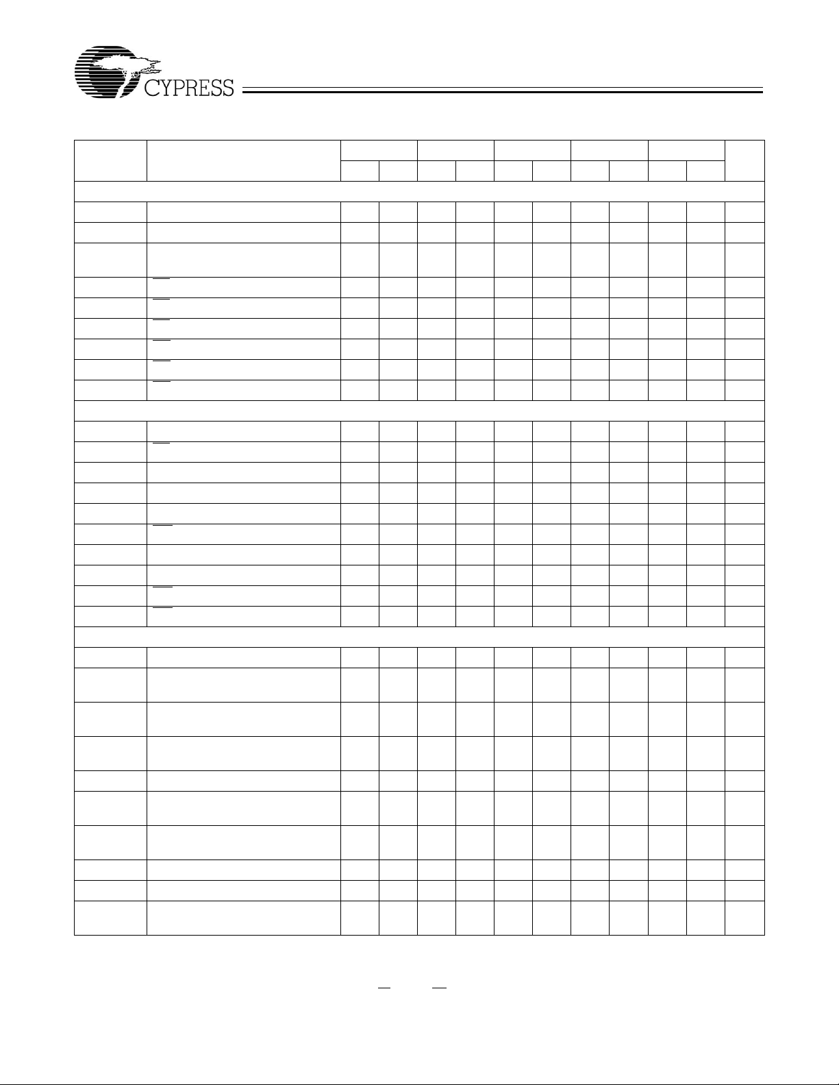
Switching Waveforms
CY7C150
ReadCycleNo.1
ADDRESS
DATA OUT PREVIOUS DATA VALID DATA VALID
[9,10]
t
OHA
t
RC
t
AA
Read CycleNo. 2
CE
[9,11]
t
RC
t
OE
ACS
t
DATA OUT
HIGH IMPEDANCE
t
LZCS
t
LZOE
DOE
DATA VALID
Write CycleNo.1(WE
Controlled)
[8]
t
SCS
t
AW
WC
t
HZWE
t
PWE
t
SD
DATA
VALID
IN
HIGH IMPEDANCE
t
HD
t
LZWE
t
HA
ADDRESS
CE
WE
DATA IN
DATA I/O
t
t
SA
DATA UNDEFINED
t
HZOE
t
HZCS
C150-5
HIGH
IMPEDANCE
C150-6
C150-7
Notes:
9. WE
is HIGH for read cycle .
10. Device is continuously selected, CS
11. Address prior to or coincident with CS
Document #: 38-05024 Rev. ** Page 4 of 11
and OE = VIL.
transition LOW.
Page 5

WWW.100Y.COM.TW WWW.100Y.COM.TW WWW.100Y.COM.TW
WWW.100Y.COM.TW WWW.100Y.COM.TW WWW.100Y.COM.TW
WWW.100Y.COM.TW WWW.100Y.COM.TW WWW.100Y.COM.TW
WWW.100Y.COM.TW WWW.100Y.COM.TW WWW.100Y.COM.TW
WWW.100Y.COM.TW WWW.100Y.COM.TW WWW.100Y.COM.TW
WWW.100Y.COM.TW WWW.100Y.COM.TW WWW.100Y.COM.TW
WWW.100Y.COM.TW WWW.100Y.COM.TW WWW.100Y.COM.TW
WWW.100Y.COM.TW WWW.100Y.COM.TW WWW.100Y.COM.TW
WWW.100Y.COM.TW WWW.100Y.COM.TW WWW.100Y.COM.TW
WWW.100Y.COM.TW WWW.100Y.COM.TW WWW.100Y.COM.TW
WWW.100Y.COM.TW WWW.100Y.COM.TW WWW.100Y.COM.TW
WWW.100Y.COM.TW WWW.100Y.COM.TW WWW.100Y.COM.TW
WWW.100Y.COM.TW WWW.100Y.COM.TW WWW.100Y.COM.TW
WWW.100Y.COM.TW WWW.100Y.COM.TW WWW.100Y.COM.TW
WWW.100Y.COM.TW WWW.100Y.COM.TW WWW.100Y.COM.TW
WWW.100Y.COM.TW WWW.100Y.COM.TW WWW.100Y.COM.TW
WWW.100Y.COM.TW WWW.100Y.COM.TW WWW.100Y.COM.TW
WWW.100Y.COM.TW WWW.100Y.COM.TW WWW.100Y.COM.TW
WWW.100Y.COM.TW WWW.100Y.COM.TW WWW.100Y.COM.TW
WWW.100Y.COM.TW WWW.100Y.COM.TW WWW.100Y.COM.TW
WWW.100Y.COM.TW WWW.100Y.COM.TW WWW.100Y.COM.TW
WWW.100Y.COM.TW WWW.100Y.COM.TW WWW.100Y.COM.TW
WWW.100Y.COM.TW WWW.100Y.COM.TW WWW.100Y.COM.TW
WWW.100Y.COM.TW WWW.100Y.COM.TW WWW.100Y.COM.TW
WWW.100Y.COM.TW WWW.100Y.COM.TW WWW.100Y.COM.TW
WWW.100Y.COM.TW WWW.100Y.COM.TW WWW.100Y.COM.TW
WWW.100Y.COM.TW WWW.100Y.COM.TW WWW.100Y.COM.TW
WWW.100Y.COM.TW WWW.100Y.COM.TW WWW.100Y.COM.TW
WWW.100Y.COM.TW WWW.100Y.COM.TW WWW.100Y.COM.TW
WWW.100Y.COM.TW WWW.100Y.COM.TW WWW.100Y.COM.TW
WWW.100Y.COM.TW WWW.100Y.COM.TW WWW.100Y.COM.TW
WWW.100Y.COM.TW WWW.100Y.COM.TW WWW.100Y.COM.TW
WWW.100Y.COM.TW WWW.100Y.COM.TW WWW.100Y.COM.TW
WWW.100Y.COM.TW WWW.100Y.COM.TW WWW.100Y.COM.TW
CY7C150
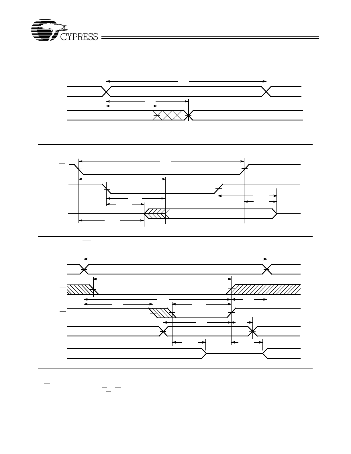
Switching Waveforms (continued)
Write CycleNo.2(CSControlled)
[8,12]
t
WC
ADDRESS
t
SA
CE
WE
t
AW
t
PWE
t
SCS
t
DATA IN
DATA I/O
DATA UNDEFINED
t
SD
DATAINVALID
HZWE
HIGH IMPEDANCE
t
HD
[13]
Reset Cycle
ADDRESS
t
RRC
WE
t
SAR
t
SWER
t
HAR
t
HWER
t
HA
C150-8
t
t
HCSR
PRS
CS
t
SCSR
RESET
DATA I/O
t
HZRS
HIGH
IMPEDANCE
t
LZRS
OUTPUT VALID ZERO
C150-9
Notes:
12. If C S
13. Reset cycle is defined by the overlap of RS
goes HIGH with WE HIGH, the output remains in a high-i mpedance state.
and CS for the minimum re set p ulse widt h.
Document #: 38-05024 Rev. ** Page 5 of 11
Page 6

WWW.100Y.COM.TW WWW.100Y.COM.TW WWW.100Y.COM.TW
WWW.100Y.COM.TW WWW.100Y.COM.TW WWW.100Y.COM.TW
WWW.100Y.COM.TW WWW.100Y.COM.TW WWW.100Y.COM.TW
WWW.100Y.COM.TW WWW.100Y.COM.TW WWW.100Y.COM.TW
WWW.100Y.COM.TW WWW.100Y.COM.TW WWW.100Y.COM.TW
WWW.100Y.COM.TW WWW.100Y.COM.TW WWW.100Y.COM.TW
WWW.100Y.COM.TW WWW.100Y.COM.TW WWW.100Y.COM.TW
WWW.100Y.COM.TW WWW.100Y.COM.TW WWW.100Y.COM.TW
WWW.100Y.COM.TW WWW.100Y.COM.TW WWW.100Y.COM.TW
WWW.100Y.COM.TW WWW.100Y.COM.TW WWW.100Y.COM.TW
WWW.100Y.COM.TW WWW.100Y.COM.TW WWW.100Y.COM.TW
WWW.100Y.COM.TW WWW.100Y.COM.TW WWW.100Y.COM.TW
WWW.100Y.COM.TW WWW.100Y.COM.TW WWW.100Y.COM.TW
WWW.100Y.COM.TW WWW.100Y.COM.TW WWW.100Y.COM.TW
WWW.100Y.COM.TW WWW.100Y.COM.TW WWW.100Y.COM.TW
WWW.100Y.COM.TW WWW.100Y.COM.TW WWW.100Y.COM.TW
WWW.100Y.COM.TW WWW.100Y.COM.TW WWW.100Y.COM.TW
WWW.100Y.COM.TW WWW.100Y.COM.TW WWW.100Y.COM.TW
WWW.100Y.COM.TW WWW.100Y.COM.TW WWW.100Y.COM.TW
WWW.100Y.COM.TW WWW.100Y.COM.TW WWW.100Y.COM.TW
WWW.100Y.COM.TW WWW.100Y.COM.TW WWW.100Y.COM.TW
WWW.100Y.COM.TW WWW.100Y.COM.TW WWW.100Y.COM.TW
WWW.100Y.COM.TW WWW.100Y.COM.TW WWW.100Y.COM.TW
WWW.100Y.COM.TW WWW.100Y.COM.TW WWW.100Y.COM.TW
WWW.100Y.COM.TW WWW.100Y.COM.TW WWW.100Y.COM.TW
WWW.100Y.COM.TW WWW.100Y.COM.TW WWW.100Y.COM.TW
WWW.100Y.COM.TW WWW.100Y.COM.TW WWW.100Y.COM.TW
WWW.100Y.COM.TW WWW.100Y.COM.TW WWW.100Y.COM.TW
WWW.100Y.COM.TW WWW.100Y.COM.TW WWW.100Y.COM.TW
WWW.100Y.COM.TW WWW.100Y.COM.TW WWW.100Y.COM.TW
WWW.100Y.COM.TW WWW.100Y.COM.TW WWW.100Y.COM.TW
WWW.100Y.COM.TW WWW.100Y.COM.TW WWW.100Y.COM.TW
WWW.100Y.COM.TW WWW.100Y.COM.TW WWW.100Y.COM.TW
WWW.100Y.COM.TW WWW.100Y.COM.TW WWW.100Y.COM.TW
Typical DC and AC Characteristics
CY7C150
NORMALIZED SUPPLY CURRENT
vs.SUPPLY VOLTAGE
1.4
1.2
I
CC SB
1.0
0.8
0.6
0.4
NORMALIZED I, I
0.2
0.0
4.0 4.5 5.0 5.5 6.0
SUPPLYVOLTAGE(V)
CC
I
SB
NORMALIZED SUPPLY CURRENT
vs.AMBIENT TEMPERATURE
1.2
1.0
CC SB
0.8
0.6
0.4
NORMALIZED I, I
0.2
I
SB
0.0
−55 25 125
AMBIENT TEMPERATURE(°C)
VCC=5.0V
V
=5.0V
IN
I
CC
OUTPUT SOURCE CURRENT
vs.OUTPUT
60
50
40
30
20
10
0
OUTPUT SOURCE CURRENT (mA)
0.0 1.0 2.0 3.0 4.0
OUTPUT VOLTAGE(V)
NORMALIZED ACCESS TIME
vs.SUPPLY
1.4
1.3
AA
1.2
1.1
1.0
NORMALIZED t
0.9
0.8
4.0 4.5 5.0 5.5 6.0
VOLTAGE
TA=25°C
SUPPLY VOLTAGE(V)
NORMALIZED ACCESS TIME
vs.AMBIENT TEMPERATURE
1.6
1.4
AA
1.2
1.0
NORMALIZED t
0.8
0.6
−55 25 125
AMBIENT TEMPERATURE(°C)
VCC=5.0V
OUTPUT SINK CURRENT
vs.OUTPUT VOLTAGE
150
125
100
75
50
25
OUTPUT SINK CURRENT (mA)
0
0.0 1.0 2.0 3.0 4.0
OUTPUT VOLTAGE(V)
VOLTAGE
V
CC
T
A
V
CC
T
A
=5.0V
=25°C
=5.0V
=25°C
5.0
TYPICALPOWER–ONCURRENT
vs.SUPPLY
3.0
2.5
PO
2.0
1.5
1.0
NORMALIZED I
0.5
0.0
0.0 1.0 2.0 3.0 4.0
VOLTAGE
SUPPLY VOLTAGE(V)
5.0
Document #: 38-05024 Rev. ** Page 6 of 11
TYPICAL ACCESS TIME CHANGE
vs.OUTPUT
30
20
AA
10
DELTA t (ns)
0
0 200 400 600 800
LOADING
=4.5V
V
CC
T
=25°C
A
CAPACITANCE (pF)
1000
NORMALIZED I
1.1
CC
1.0
0.9
NORMALIZED I
0.8
=5.0V
V
CC
T
=25°C
A
V
=0.5V
CC
10 20 30 40
CYCLE FREQUENCY (MHz)
vs.CYCLETIME
CC
Page 7

WWW.100Y.COM.TW WWW.100Y.COM.TW WWW.100Y.COM.TW
WWW.100Y.COM.TW WWW.100Y.COM.TW WWW.100Y.COM.TW
WWW.100Y.COM.TW WWW.100Y.COM.TW WWW.100Y.COM.TW
WWW.100Y.COM.TW WWW.100Y.COM.TW WWW.100Y.COM.TW
WWW.100Y.COM.TW WWW.100Y.COM.TW WWW.100Y.COM.TW
WWW.100Y.COM.TW WWW.100Y.COM.TW WWW.100Y.COM.TW
WWW.100Y.COM.TW WWW.100Y.COM.TW WWW.100Y.COM.TW
WWW.100Y.COM.TW WWW.100Y.COM.TW WWW.100Y.COM.TW
WWW.100Y.COM.TW WWW.100Y.COM.TW WWW.100Y.COM.TW
WWW.100Y.COM.TW WWW.100Y.COM.TW WWW.100Y.COM.TW
WWW.100Y.COM.TW WWW.100Y.COM.TW WWW.100Y.COM.TW
WWW.100Y.COM.TW WWW.100Y.COM.TW WWW.100Y.COM.TW
WWW.100Y.COM.TW WWW.100Y.COM.TW WWW.100Y.COM.TW
WWW.100Y.COM.TW WWW.100Y.COM.TW WWW.100Y.COM.TW
WWW.100Y.COM.TW WWW.100Y.COM.TW WWW.100Y.COM.TW
WWW.100Y.COM.TW WWW.100Y.COM.TW WWW.100Y.COM.TW
WWW.100Y.COM.TW WWW.100Y.COM.TW WWW.100Y.COM.TW
WWW.100Y.COM.TW WWW.100Y.COM.TW WWW.100Y.COM.TW
WWW.100Y.COM.TW WWW.100Y.COM.TW WWW.100Y.COM.TW
WWW.100Y.COM.TW WWW.100Y.COM.TW WWW.100Y.COM.TW
WWW.100Y.COM.TW WWW.100Y.COM.TW WWW.100Y.COM.TW
WWW.100Y.COM.TW WWW.100Y.COM.TW WWW.100Y.COM.TW
WWW.100Y.COM.TW WWW.100Y.COM.TW WWW.100Y.COM.TW
WWW.100Y.COM.TW WWW.100Y.COM.TW WWW.100Y.COM.TW
WWW.100Y.COM.TW WWW.100Y.COM.TW WWW.100Y.COM.TW
WWW.100Y.COM.TW WWW.100Y.COM.TW WWW.100Y.COM.TW
WWW.100Y.COM.TW WWW.100Y.COM.TW WWW.100Y.COM.TW
WWW.100Y.COM.TW WWW.100Y.COM.TW WWW.100Y.COM.TW
WWW.100Y.COM.TW WWW.100Y.COM.TW WWW.100Y.COM.TW
WWW.100Y.COM.TW WWW.100Y.COM.TW WWW.100Y.COM.TW
WWW.100Y.COM.TW WWW.100Y.COM.TW WWW.100Y.COM.TW
WWW.100Y.COM.TW WWW.100Y.COM.TW WWW.100Y.COM.TW
WWW.100Y.COM.TW WWW.100Y.COM.TW WWW.100Y.COM.TW
WWW.100Y.COM.TW WWW.100Y.COM.TW WWW.100Y.COM.TW
Truth Table
Inputs
Outputs ModeCS WE OE RS
H X X X High Z Not Selected
L H X L High Z Reset
L L X H High Z Write
L H L H O0−O
L X H H High Z Output Disable
3
Read
Ordering Information
Speed
(ns) Ordering Code
10 CY7C150−10PC P13A 24-Lead (300-Mil) Molded DIP Commercial
CY7C150−10SC S13 24-Lead Molded SOIC
12 CY7C150−12PC P13A 24-Lead (300-Mil) Molded DIP Commercial
CY7C150−12SC S13 24-Lead Molded SOIC
CY7C150−12DMB D14 24-Lead (300-Mil) CerDIP Military
15 CY7C150−15PC P13A 24-Lead (300-Mil) Molded DIP Commercial
CY7C150−15SC S13 24-Lead Molded SOIC
CY7C150−15DMB D14 24-Lead (300-Mil) CerDIP Military
25 CY7C150−25PC P13A 24-Lead (300-Mil) Molded DIP Commercial
35 CY7C150−35DMB D14 24-Lead (300-Mil) CerDIP Military
CY7C150−25SC S13 24-Lead Molded SOIC
CY7C150−25DMB D14 24-Lead (300-Mil) CerDIP Military
Package
Name Package Type
Operating
Range
CY7C150
Document #: 38-05024 Rev. ** Page 7 of 11
Page 8

WWW.100Y.COM.TW WWW.100Y.COM.TW WWW.100Y.COM.TW
WWW.100Y.COM.TW WWW.100Y.COM.TW WWW.100Y.COM.TW
WWW.100Y.COM.TW WWW.100Y.COM.TW WWW.100Y.COM.TW
WWW.100Y.COM.TW WWW.100Y.COM.TW WWW.100Y.COM.TW
WWW.100Y.COM.TW WWW.100Y.COM.TW WWW.100Y.COM.TW
WWW.100Y.COM.TW WWW.100Y.COM.TW WWW.100Y.COM.TW
WWW.100Y.COM.TW WWW.100Y.COM.TW WWW.100Y.COM.TW
WWW.100Y.COM.TW WWW.100Y.COM.TW WWW.100Y.COM.TW
WWW.100Y.COM.TW WWW.100Y.COM.TW WWW.100Y.COM.TW
WWW.100Y.COM.TW WWW.100Y.COM.TW WWW.100Y.COM.TW
WWW.100Y.COM.TW WWW.100Y.COM.TW WWW.100Y.COM.TW
WWW.100Y.COM.TW WWW.100Y.COM.TW WWW.100Y.COM.TW
WWW.100Y.COM.TW WWW.100Y.COM.TW WWW.100Y.COM.TW
WWW.100Y.COM.TW WWW.100Y.COM.TW WWW.100Y.COM.TW
WWW.100Y.COM.TW WWW.100Y.COM.TW WWW.100Y.COM.TW
WWW.100Y.COM.TW WWW.100Y.COM.TW WWW.100Y.COM.TW
WWW.100Y.COM.TW WWW.100Y.COM.TW WWW.100Y.COM.TW
WWW.100Y.COM.TW WWW.100Y.COM.TW WWW.100Y.COM.TW
WWW.100Y.COM.TW WWW.100Y.COM.TW WWW.100Y.COM.TW
WWW.100Y.COM.TW WWW.100Y.COM.TW WWW.100Y.COM.TW
WWW.100Y.COM.TW WWW.100Y.COM.TW WWW.100Y.COM.TW
WWW.100Y.COM.TW WWW.100Y.COM.TW WWW.100Y.COM.TW
WWW.100Y.COM.TW WWW.100Y.COM.TW WWW.100Y.COM.TW
WWW.100Y.COM.TW WWW.100Y.COM.TW WWW.100Y.COM.TW
WWW.100Y.COM.TW WWW.100Y.COM.TW WWW.100Y.COM.TW
WWW.100Y.COM.TW WWW.100Y.COM.TW WWW.100Y.COM.TW
WWW.100Y.COM.TW WWW.100Y.COM.TW WWW.100Y.COM.TW
WWW.100Y.COM.TW WWW.100Y.COM.TW WWW.100Y.COM.TW
WWW.100Y.COM.TW WWW.100Y.COM.TW WWW.100Y.COM.TW
WWW.100Y.COM.TW WWW.100Y.COM.TW WWW.100Y.COM.TW
WWW.100Y.COM.TW WWW.100Y.COM.TW WWW.100Y.COM.TW
WWW.100Y.COM.TW WWW.100Y.COM.TW WWW.100Y.COM.TW
WWW.100Y.COM.TW WWW.100Y.COM.TW WWW.100Y.COM.TW
WWW.100Y.COM.TW WWW.100Y.COM.TW WWW.100Y.COM.TW
CY7C150
MILITAR Y SPECIFICATIONS
Group A Subgroup Testing
DC Characteristics
Parameter Subgroups
V
OH
V
OL
V
IH
V
Max. 1, 2, 3
IL
I
IX
I
OZ
I
CC
1, 2, 3
1, 2, 3
1, 2, 3
1, 2, 3
1, 2, 3
1, 2, 3
Switching Characteristics
Parameter Subgroups
READ CYCLE
t
RC
t
AA
t
OHA
t
ACS
WRITE CYCLE
t
WC
t
SCS
t
AW
t
HA
t
SA
t
PWE
t
SD
t
HD
RESET CYCLE
t
RRC
t
SAR
t
SWER
t
SCSR
t
PRS
t
HCSR
t
HWER
t
HAR
7, 8, 9, 10, 11
7, 8, 9, 10, 11
7, 8, 9, 10, 11
7, 8, 9, 10, 11
7, 8, 9, 10, 11
7, 8, 9, 10, 11
7, 8, 9, 10, 11
7, 8, 9, 10, 11
7, 8, 9, 10, 11
7, 8, 9, 10, 11
7, 8, 9, 10, 11
7, 8, 9, 10, 11
7, 8, 9, 10, 11
7, 8, 9, 10, 11
7, 8, 9, 10, 11
7, 8, 9, 10, 11
7, 8, 9, 10, 11
7, 8, 9, 10, 11
7, 8, 9, 10, 11
7, 8, 9, 10, 11
Document #: 38-05024 Rev. ** Page 8 of 11
Page 9

WWW.100Y.COM.TW WWW.100Y.COM.TW WWW.100Y.COM.TW
WWW.100Y.COM.TW WWW.100Y.COM.TW WWW.100Y.COM.TW
WWW.100Y.COM.TW WWW.100Y.COM.TW WWW.100Y.COM.TW
WWW.100Y.COM.TW WWW.100Y.COM.TW WWW.100Y.COM.TW
WWW.100Y.COM.TW WWW.100Y.COM.TW WWW.100Y.COM.TW
WWW.100Y.COM.TW WWW.100Y.COM.TW WWW.100Y.COM.TW
WWW.100Y.COM.TW WWW.100Y.COM.TW WWW.100Y.COM.TW
WWW.100Y.COM.TW WWW.100Y.COM.TW WWW.100Y.COM.TW
WWW.100Y.COM.TW WWW.100Y.COM.TW WWW.100Y.COM.TW
WWW.100Y.COM.TW WWW.100Y.COM.TW WWW.100Y.COM.TW
WWW.100Y.COM.TW WWW.100Y.COM.TW WWW.100Y.COM.TW
WWW.100Y.COM.TW WWW.100Y.COM.TW WWW.100Y.COM.TW
WWW.100Y.COM.TW WWW.100Y.COM.TW WWW.100Y.COM.TW
WWW.100Y.COM.TW WWW.100Y.COM.TW WWW.100Y.COM.TW
WWW.100Y.COM.TW WWW.100Y.COM.TW WWW.100Y.COM.TW
WWW.100Y.COM.TW WWW.100Y.COM.TW WWW.100Y.COM.TW
WWW.100Y.COM.TW WWW.100Y.COM.TW WWW.100Y.COM.TW
WWW.100Y.COM.TW WWW.100Y.COM.TW WWW.100Y.COM.TW
WWW.100Y.COM.TW WWW.100Y.COM.TW WWW.100Y.COM.TW
WWW.100Y.COM.TW WWW.100Y.COM.TW WWW.100Y.COM.TW
WWW.100Y.COM.TW WWW.100Y.COM.TW WWW.100Y.COM.TW
WWW.100Y.COM.TW WWW.100Y.COM.TW WWW.100Y.COM.TW
WWW.100Y.COM.TW WWW.100Y.COM.TW WWW.100Y.COM.TW
WWW.100Y.COM.TW WWW.100Y.COM.TW WWW.100Y.COM.TW
WWW.100Y.COM.TW WWW.100Y.COM.TW WWW.100Y.COM.TW
WWW.100Y.COM.TW WWW.100Y.COM.TW WWW.100Y.COM.TW
WWW.100Y.COM.TW WWW.100Y.COM.TW WWW.100Y.COM.TW
WWW.100Y.COM.TW WWW.100Y.COM.TW WWW.100Y.COM.TW
WWW.100Y.COM.TW WWW.100Y.COM.TW WWW.100Y.COM.TW
WWW.100Y.COM.TW WWW.100Y.COM.TW WWW.100Y.COM.TW
WWW.100Y.COM.TW WWW.100Y.COM.TW WWW.100Y.COM.TW
WWW.100Y.COM.TW WWW.100Y.COM.TW WWW.100Y.COM.TW
WWW.100Y.COM.TW WWW.100Y.COM.TW WWW.100Y.COM.TW
WWW.100Y.COM.TW WWW.100Y.COM.TW WWW.100Y.COM.TW
Package Diagrams
CY7C150
24-Lead(300-Mil) CerDIP D14
MIL-STD-1835 D- 9Config.A
24-Lead (300-Mil) MoldedDIP P13/P13A
Document #: 38-05024 Rev. ** Page 9 of 11
Page 10

ng so indemnifies Cypress Semiconductor against all charges.
WWW.100Y.COM.TW WWW.100Y.COM.TW WWW.100Y.COM.TW
WWW.100Y.COM.TW WWW.100Y.COM.TW WWW.100Y.COM.TW
WWW.100Y.COM.TW WWW.100Y.COM.TW WWW.100Y.COM.TW
WWW.100Y.COM.TW WWW.100Y.COM.TW WWW.100Y.COM.TW
WWW.100Y.COM.TW WWW.100Y.COM.TW WWW.100Y.COM.TW
WWW.100Y.COM.TW WWW.100Y.COM.TW WWW.100Y.COM.TW
WWW.100Y.COM.TW WWW.100Y.COM.TW WWW.100Y.COM.TW
WWW.100Y.COM.TW WWW.100Y.COM.TW WWW.100Y.COM.TW
WWW.100Y.COM.TW WWW.100Y.COM.TW WWW.100Y.COM.TW
WWW.100Y.COM.TW WWW.100Y.COM.TW WWW.100Y.COM.TW
WWW.100Y.COM.TW WWW.100Y.COM.TW WWW.100Y.COM.TW
WWW.100Y.COM.TW WWW.100Y.COM.TW WWW.100Y.COM.TW
WWW.100Y.COM.TW WWW.100Y.COM.TW WWW.100Y.COM.TW
WWW.100Y.COM.TW WWW.100Y.COM.TW WWW.100Y.COM.TW
WWW.100Y.COM.TW WWW.100Y.COM.TW WWW.100Y.COM.TW
WWW.100Y.COM.TW WWW.100Y.COM.TW WWW.100Y.COM.TW
WWW.100Y.COM.TW WWW.100Y.COM.TW WWW.100Y.COM.TW
WWW.100Y.COM.TW WWW.100Y.COM.TW WWW.100Y.COM.TW
WWW.100Y.COM.TW WWW.100Y.COM.TW WWW.100Y.COM.TW
WWW.100Y.COM.TW WWW.100Y.COM.TW WWW.100Y.COM.TW
WWW.100Y.COM.TW WWW.100Y.COM.TW WWW.100Y.COM.TW
WWW.100Y.COM.TW WWW.100Y.COM.TW WWW.100Y.COM.TW
WWW.100Y.COM.TW WWW.100Y.COM.TW WWW.100Y.COM.TW
WWW.100Y.COM.TW WWW.100Y.COM.TW WWW.100Y.COM.TW
WWW.100Y.COM.TW WWW.100Y.COM.TW WWW.100Y.COM.TW
WWW.100Y.COM.TW WWW.100Y.COM.TW WWW.100Y.COM.TW
WWW.100Y.COM.TW WWW.100Y.COM.TW WWW.100Y.COM.TW
WWW.100Y.COM.TW WWW.100Y.COM.TW WWW.100Y.COM.TW
WWW.100Y.COM.TW WWW.100Y.COM.TW WWW.100Y.COM.TW
WWW.100Y.COM.TW WWW.100Y.COM.TW WWW.100Y.COM.TW
WWW.100Y.COM.TW WWW.100Y.COM.TW WWW.100Y.COM.TW
WWW.100Y.COM.TW WWW.100Y.COM.TW WWW.100Y.COM.TW
WWW.100Y.COM.TW WWW.100Y.COM.TW WWW.100Y.COM.TW
WWW.100Y.COM.TW WWW.100Y.COM.TW WWW.100Y.COM.TW
CY7C150
Package Diagrams (continued)
24-Lead Molded SOICS13
Document #: 38-05024 Rev. ** Page 10 of 11
© Cypress Semiconductor Corporation, 2001. The information contained herein is subject to change without notice. Cypress Semiconductor Corporation assumes no responsibility for the use
of any circuitry other than circuitry embodied in a Cypress Semiconductor product. Nor does it convey or imply any license unde r patent or other rights. Cypress Semiconductor does not autho rize
its products for use as critical components in life-support systems where a malfunction or failure may reasonably be expected to result in significant injury to the user. The inclusion of Cypress
Semiconductor products in life-support systems application implies that the manufacturer assume s all risk of such use and in doi
Page 11

CY7C150
WWW.100Y.COM.TW WWW.100Y.COM.TW WWW.100Y.COM.TW
WWW.100Y.COM.TW WWW.100Y.COM.TW WWW.100Y.COM.TW
WWW.100Y.COM.TW WWW.100Y.COM.TW WWW.100Y.COM.TW
WWW.100Y.COM.TW WWW.100Y.COM.TW WWW.100Y.COM.TW
Document Title: Cy7C150 1K x4 Static RAM
Document Number: 38-05024
REV. ECN NO.
** 106810 09/10/01 SZV Change from Spec number: 38-00028 to 38-05024
Issue
Date
Orig. of
Change Description of Change
WWW.100Y.COM.TW WWW.100Y.COM.TW WWW.100Y.COM.TW
WWW.100Y.COM.TW WWW.100Y.COM.TW WWW.100Y.COM.TW
WWW.100Y.COM.TW WWW.100Y.COM.TW WWW.100Y.COM.TW
WWW.100Y.COM.TW WWW.100Y.COM.TW WWW.100Y.COM.TW
 Loading...