

Page 1
399B
CY7C1399B
32K x 8 3.3V Static RAM
Features
• Single 3.3V power supply
• Ideal for low-voltage cache memory applications
• High speed
—10/12/15 ns
• Low active power
—216 mW (max.)
• Low-power alpha immune 6T cell
• Plastic SOJ and TSOP packaging
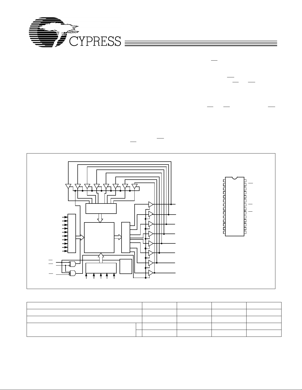
Functional Description
The CY7C1399B is a high-performance 3.3V CMOS Static
RAM organize d as 3 2,7 68 wo rd s b y 8 bi ts. E asy me m or y expansion is provided by an active LOW Chip Enable (CE
) and
Logic Block Diagram
INPUTBUFFER
A
0
A
1
A
2
A
3
A
CE
WE
OE
4
A
5
A
6
A
A
A
ROW DECODER
7
8
9
10
A
32K x 8
ARRAY
COLUMN
DECODER
11A13A12
A
14
A
SENSE AMPS
POWER
DOWN
active LOW Output Enable (OE
) and three-state drivers. The
device has an automatic power-down feature, reducing the
power consumption by more than 95% when deselected.
An active LOW Write Enab le signal (WE
) controls the writing/
reading operation of the memor y . When CE and WE inputs are
both LOW, data on the eight data input/output pins (I/O
through I/O7) is written into the memory locati on addressed by
the address present on the address pins (A0 through A14).
Reading th e device is ac complished by selectin g the device
and enabling the outputs, CE
and OE active LOW, while WE
remains inactive or HIGH. Under these conditions, the contents of the location addressed by the information on address
pins is present on the eight data input/output pins.
The input/output pi ns remain in a hig h-impedance sta te unless
the chip is selected, outputs are enabled, and Write Enable
) is HIGH. The CY7C1399B is availab le in 28-pin standard
(WE
300-mil-wide SOJ and TSOP Type I packages.
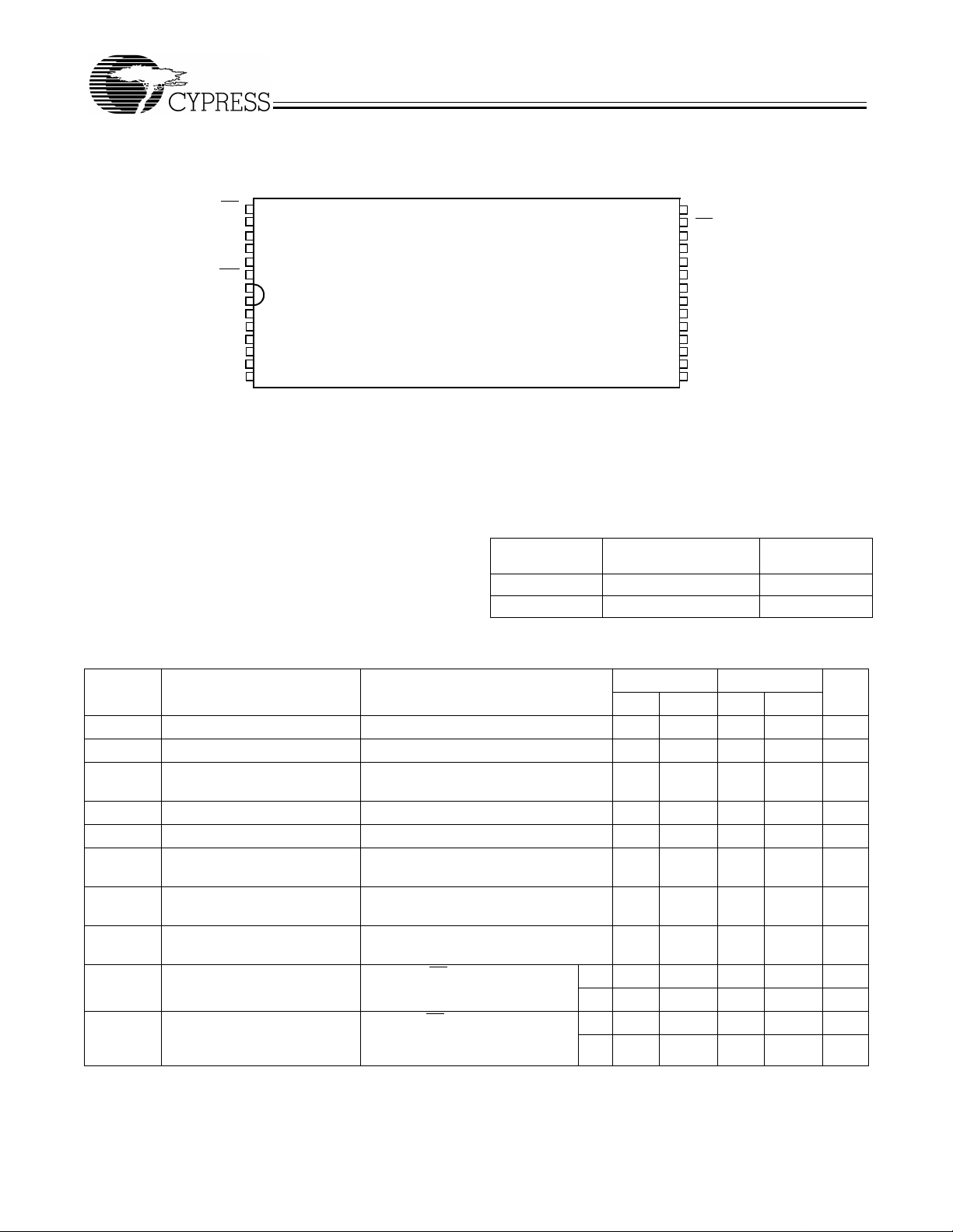
Pin Configurations
SOJ
Top View
V
28
CC
WE
27
26
A
4
25
A
3
24
A
2
23
A
1
22
OE
21
A
0
20
CE
19
I/O
7
18
I/O
6
17
I/O
5
16
I/O
4
15
I/O
3
I/O
I/O
I/O
I/O
I/O
I/O
I/O
I/O
A
1
5
A
6
2
A
3
7
A
8
4
A
5
9
A
10
6
A
11
0
1
2
3
4
5
6
7
A
A
A
I/O
I/O
I/O
GND
7
12
8
13
9
10
14
11
0
12
1
13
2
14
0
Selection Guide
1399B-10 1399B-12 1399B-15 1399B-20
Maximum Access Time (ns) 10 12 15 20
Maximum Operating Current (mA) 60 55 50 45
Maximum CMOS Standby Current (µA) 500 500 500 500
L50
Cypress Semiconductor Corporation • 3901 North First Street • San Jose • CA 95134 • 408-943-2600
Document #: 38-05071 Rev. *A Revised June 19, 2001
50 50 50
Page 2
Pin Configuration
OE
WE
V
A
A
A
A
A
A
CC
A
A
A7
A
A
CY7C1399B
TSOP
Top View
22
23
1
24
2
25
3
26
4
27
28
1
5
2
6
3
4
8
5
9
6
10
7
11
21
A
0
20
CE
19
I/O
7
18
I/O
6
17
I/O
5
16
I/O
4
I/O
15
3
14
GND
13
I/O
2
12
I/O
1
11
I/O
0
10
A
14
9
A
13
8
A
12
Maximum Ratings
(Above which the useful life may be im pai red. For user guidelines, not tested.)
Storage Temperature .................................–65°C to +150°C
Ambient Temperature with
Power Applied.............................................–55°C to +125°C
Supply Voltage on V
DC Voltage Applied to Outputs
in High Z State
[1]
DC Input Voltage
to Relative GND
CC
....................................–0.5V to VCC + 0.5V
[1]
................................–0.5V to VCC + 0.5V
[1]
....–0.5V to +4.6V
Electrical Characteristics Ov er the Op erat ing Range
Output Current into Outputs (LOW).............................20 mA
Static Discharge Voltage.......................................... >2001V
(per MIL-STD-883, Method 3015)
Latch-Up Current.................................................... >200 mA
Operating Range
Range
Commercial 0°C to +70°C 3.3V ±300 mV
Industrial –40°C to +85°C 3.3V ±300 mV
[1]
Ambient
Temperature V
CC
7C1399B-10 7C1399B-12
Parameter Description Test Conditions Min. Max. Min. Max. Unit
V
OH
V
OL
V
IH
V
IL
I
IX
I
OZ
I
OS
I
CC
I
SB1
I
SB2
Notes:
1. Minimum voltage is equal to –2.0V for pulse durations of less than 20 ns.
2. Not more than one output should be shorted at one time. Duration of the short circuit should not exceed 30 seconds.
3. Device draws low standby current regardless of switching on the addresses.
Output HIGH Voltage VCC = Min., IOH = –2.0 mA 2.4 2.4 V
Output LOW Voltage VCC = Min., IOL = 4.0 mA 0.4 0.4 V
Input HIGH Voltage 2.2 V
+0.3V
CC
2.2 V
+0.3V
CC
Input LOW Voltage –0.3 0.8 –0.3 0.8 V
Input Load Current –1+1–1 +1 µA
Output Leakage
Current
Output Short
Circuit Current
[2]
VCC Operatin g
Supply Current
Automatic CE Power-Down
Current — TTL Inputs
Automatic CE Power-Down
Current — CMOS Inputs
[3]
GND ≤ VI ≤ VCC,
Output Dis abled
VCC = Max., V
VCC = Max., I
f = f
= 1/t
MAX
= GND –300 –300 mA
OUT
= 0 mA,
OUT
RC
Max. VCC, CE ≥ VIH,
≥ VIH, or V
V
IN
Max. VCC, CE ≥ V
– 0.3V , or V
WE ≥V
CC
≤ VIL,f = f
IN
CC
≤ 0.3V ,
IN
– 0.3V or WE ≤0.3V, f= f
MAX
– 0.3V , VIN ≥ VCC
MAX
–5+5–5 +5 µA
60 55 mA
5 5 mA
L44 mA
500 500 µA
L5050 µA
V
Document #: 38-05071 Rev. *A Page 2 of 10
Page 3
CY7C1399B
Electrical Characteristics Over the Operating Range (continued)
1399B-15 1399B-20
Parameter Description Test Conditions Min. Max. Min. Max. Unit
V
V
V
V
I
IX
I
OZ
I
OS
I
CC
I
SB1
I
SB2
OH
OL
IH
IL
Output HIGH Voltage VCC = Min., IOH = –2.0 mA 2.4 2.4 V
Output LOW Voltage VCC = Min., IOL = 4.0 mA 0.4 0.4 V
Input HIGH Voltage 2.2 V
+0.3V
CC
2.2 V
+0.3V
CC
Input LOW Voltage –0.3 0.8 –0.3 0.8 V
Input Load Current –1 +1 –1 +1 µA
Output Leakage Current GND ≤ VI ≤ VCC,
–5 +5 –5 +5 µA
Output Disabled
Output Short Circuit
[2]
Current
VCC Operating
Supply Current
Automatic CE Power-Down
Current — TTL Inputs
Automatic CE Power-Down
Current — CMOS Inputs
VCC = Max., V
VCC = Max., I
= 1/t
f = f
MAX
= GND –300 –300 mA
OUT
= 0 mA,
OUT
RC
Max. VCC, CE ≥ VIH,
≥ VIH, or V
V
IN
f = f
MAX
Max. VCC, CE ≥ VCC–0.3V , VIN ≥
[3]
– 0.3V , or VIN ≤ 0. 3V,
V
CC
WE≥V
CC
f=f
MAX
≤ VIL,
IN
–0.3V or WE≤ 0.3V,
50 45 mA
5 5 mA
L 4 4 mA
500 500 µA
L 50 50 µA
V
Capacitance
[4]
Parameter Description Test Conditions Max. Unit
CIN: Address es Input Capacitance TA = 25°C, f = 1 MHz, VCC = 3.3V 5 pF
CIN: Controls 6 pF
C
OUT
Output Capacitance 6 pF
AC Test Loads and Waveforms
Ω
167
R1 317
3.0V
C
L
Ω
R2
351
Ω
GND
10%
≤ 3ns
ALL INPUT PULSES
90%
90%
10%
3.3V
OUTPUT
INCLUDING
JIG AND
SCOPE
Equivalent to: THÉVENIN EQUIVALENT
OUTPUT 1.73V
Note:
4. Tested initially and after any design or process changes that may affect these parameters.
≤ 3 ns
Document #: 38-05071 Rev. *A Page 3 of 10
Page 4

CY7C1399B
Switching Characteristics O ver the Operating Range
[5]
1399B–10 1399B–12
Parameter Description Min. Max. Min. Max. Unit
READ CYCLE
t
RC
t
AA
t
OHA
t
ACE
t
DOE
t
LZOE
t
HZOE
t
LZCE
t
HZCE
t
PU
t
PD
WRITE CYCLE
t
WC
t
SCE
t
AW
t
HA
t
SA
t
PWE
t
SD
t
HD
t
HZWE
t
LZWE
Notes:
5. Test conditions assume signal transition time of 3 ns or less, timing reference levels of 1.5V, input pulse levels of 0 to 3.0V, and output loading of the specified
I
and capacitance CL = 30 pF .
OL/IOH
6. At any given temperature and voltage condition, t
8. The internal write time of the memory is defined by the overlap of CE
9. The minimum write cycle time for write cycle #3 (WE
, t
7. t
HZOE
HZCE
a write by going HIGH. The data input set -up and hold timing sho uld be referenced to the rising edge of the sign al that termin ates the write.
Read Cycle Time 10 12 ns
Address to Data Valid 10 12 ns
Data Hold from Address Change 3 3 ns
CE LOW to Data Valid 10 12 ns
OE LOW to Data Valid 5 5 ns
OE LOW to Low Z
OE HIGH to High Z
CE LOW to Low Z
CE HIGH to High Z
[6]
[6]
[6, 7]
[6, 7]
00ns
55ns
33ns
56ns
CE LOW to Power-Up 0 0 ns
CE HIGH to Power-Down 10 12 ns
[8, 9]
Write Cycle Time 10 12 ns
CE LOW to Write End 8 8 ns
Address Set-Up to Write End 7 8 ns
Address Hold from Write End 0 0 ns
Address Set-Up to Write Start 0 0 ns
WE Pulse Width 7 8 ns
Data Set-Up to Write End 5 7 ns
Data Hold from Write End 0 0 ns
WE LOW to High Z
WE HIGH to Low Z
, t
are specified wi th CL = 5 pF as in AC T est Loads. T ransit ion is measured ±50 0 mV from steady state vo ltage.
HZWE
[8]
[6]
is less than t
HZCE
controlled, OE LOW) is the sum of t
LZCE
LOW and WE LOW . Bot h signals must be L OW to initi ate a writ e and eit her signal can terminat e
, t
HZOE
is less than t
HZWE
77ns
33ns
LZOE
and tSD.
, and t
HZWE
is less than t
for any given device.
LZWE
Document #: 38-05071 Rev. *A Page 4 of 10
Page 5

CY7C1399B
Switching Characteristics O ver the Operating Range
[5]
(Continued)
1399B–15 1399B–20
Parameter Description Min. Max. Min. Max. Unit
READ CYCLE
t
RC
t
AA
t
OHA
t
ACE
t
DOE
t
LZOE
t
HZOE
t
LZCE
t
HZCE
t
PU
t
PD
WRITE CYCLE
t
WC
t
SCE
t
AW
t
HA
t
SA
t
PWE
t
SD
t
HD
t
HZWE
t
LZWE
Read Cycle Time 15 20 ns
Address to Data Valid 15 20 ns
Data Hold from Address Change 3 3 ns
CE LOW to Data Valid 15 20 ns
OE LOW to Data Valid 6 7 ns
OE LOW to Low Z
OE HIGH to High Z
CE LOW to Low Z
CE HIGH to High Z
[6]
[6]
[6, 7]
[6, 7]
0 0 ns
6 6 ns
3 3 ns
7 7 ns
CE LOW to Power-Up 0 0 ns
CE HIGH to Power-Down 15 20 ns
[8, 9]
Write Cycle Time 15 20 ns
CE LOW to Write End 10 12 ns
Address Set-Up to Write End 10 12 ns
Address Hold from Write End 0 0 ns
Address Set-Up to Write Start 0 0 ns
WE Pulse Width 10 12 ns
Data Set-Up to Write End 8 10 ns
Data Hold from Write End 0 0 ns
WE LOW to High Z
WE HIGH to Low Z
[8]
[6]
7 7 ns
3 3 ns
Data Retention Characteristics (Over the Operating Range - L version only)
Parameter Description Conditions Min. Max. Unit
V
DR
I
CCDR
t
CDR
t
R
Document #: 38-05071 Rev. *A Page 5 of 10
VCC for Data Retention 2.0 V
Data Retention Current Com’l VCC = VDR = 2.0V ,
Chip Deselect to Data
Retention Time
Operation Recovery Time t
CE > VCC – 0.3V ,
> VCC – 0.3V or
V
IN
< 0.3V
V
IN
0 20 uA
0 ns
RC
ns
Page 6

Data Retention Waveform
V
CC
CE
Switching Waveforms
t
CDR
DATA RETENTION MODE
V
> 2V
DR
CY7C1399B
3.0V3.0V
t
R
Read Cycle No. 1
[10, 11]
ADDRESS
DATA OUT PREVIOUS DATA VALID
Read Cycle No. 2
[11, 12 ]
CE
t
OE
t
DATA OUT
V
CC
SUPPLY
HIGH IMPEDANCE
t
LZCE
t
PU
CURRENT
ACE
LZOE
t
OHA
t
50%
DOE
t
RC
t
AA
DATA VALID
t
RC
t
HZOE
t
DATA VALID
HZCE
t
PD
HIGH
IMPEDANCE
ICC
50%
ISB
Notes:
10. Device is continuously selected. OE
11. WE
is HIGH for read cycle .
12. Address valid prior to or coi ncident with CE
, CE = VIL.
transition LOW .
Document #: 38-05071 Rev. *A Page 6 of 10
Page 7

Switching Waveforms (continued)
CY7C1399B
Write Cycle No. 1 (WE Controlled)
ADDRESS
CE
t
WE
SA
OE
DATA I/O
NOTE 15
Write Cycle No. 2 (C E Controlle d)
ADDRESS
CE
[8, 13, 14]
t
HZOE
[8, 13, 14]
t
WC
t
AW
t
PWE
t
SD
DATAINVALID
t
WC
t
SCE
t
SA
t
AW
t
HA
t
HD
t
HA
WE
DATA I/O
Write Cycle No. 3 (WE Controlled, OE LOW)
[9, 14]
t
WC
DATAINVALID
ADDRESS
CE
t
AW
t
WE
DATA I/O
Notes:
13. Data I/O is high impedance if OE
14. If C E
15. During this period, the I/Os are in the output state and input signals should not be applied.
goes HIGH simultaneousl y with WE HIGH, the ou tput r emains in a hi gh-impeda nce s tate.
SA
NOTE 15
= VIH.
t
HZWE
t
SD
t
SD
DATAINVALID
t
HD
t
HA
t
HD
t
LZWE
Document #: 38-05071 Rev. *A Page 7 of 10
Page 8

CY7C1399B
Truth Table
CE WE OE Input/Output Mode Power
H X X High Z Deselect/Power-Down Standby (ISB)
L H L Data Out Read Active (ICC)
L L X Data In Write Active (ICC)
L H H High Z Deselect, Output Disabled Active (ICC)
Ordering Information
Speed
(ns) Ordering Code
10 CY7C1399B-10VC V21 28-Lead Molded SOJ Commercial
CY7C1399B-10ZC Z28 28-Lead Thin Small Outline Package
CY7C1399BL-10VC V21
CY7C1399BL-10ZC Z28 28-Lead Thin Small Outline Package
12 CY7C1399B–12V C V21 28-Lead Molded SOJ
CY7C1399B–12ZC Z28 28-Lead Thin Small Outline Package
CY7C1399BL-12VC V21 28-Lead Molded SOJ
CY7C1399BL-12ZC Z28 28-Lead Thin Small Outline Package
CY7C1399B–12VI V21 28-Lead Mo lde d SOJ Industrial
CY7C1399B–12ZI Z28 28-Lead Thin Small Outline Package
15 CY7C1399B–15VC V21 28-Lead Molded SOJ Commercial
CY7C1399B–15ZC Z28 28-Lead Thin Small Outline Package
CY7C1399BL-15VC V21 28-Lead Molded SOJ
CY7C1399BL-15ZC Z28 28-Lead Thin Small Outline Package
CY7C1399B–15VI V21 28-Lead Molded SOJ Industrial
CY7C1399B–15ZI Z28 28-Lead Thin Small Outline Package
20 CY7C1399B–20VC V21 28-Lead Molded SOJ Commercial
CY7C1399B–20ZC Z28 28-Lead Thin Small Outline Package
CY7C1399BL-20VC V21 28-Lead Molded SOJ
CY7C1399BL-20ZC Z28 28-Lead Thin Small Outline Package
CY7C1399B–20VI V21 28-Lead Molded SOJ Industrial
CY7C1399B–20ZI Z28 28-Lead Thin Small Outline Package
Package
Name Package Type
28-Lead Molded SOJ
Operating
Range
Document #: 38-05071 Rev. *A Page 8 of 10
Page 9

ng so indemnifies Cypress Semiconductor against all charges.
Package Diagrams
CY7C1399B
28-Lead (300-Mil) Molded SOJ V21
28-Lead Thin Small Outline Package Type 1 (8x13.4 mm) Z28
51-85031-B
Document #: 38-05071 Rev. *A Page 9 of 10
© Cypress Semiconductor Corporation, 2001. The information contained herein is subject to change without notice. Cypress Semiconductor Corporation assumes no responsibility for the use
of any circuitry other than circuitry embodied in a Cypress Semiconductor product. No r does it convey or imply any license under patent or other rights. Cypress Semiconductor does not autho rize
its products for use as critical components in life-support systems where a malfunction or failure may reasonably be expected to result in significant injury to the user. The inclusion of Cypress
Semiconductor products in life-support systems application implies that the manufacturer assume s all risk of such use and in doi
51-85071-*G
Page 10

Revision History
Document Title: CY7C1399B 32K x 8 3.3V Static RAM
Document Number: 38-05071
CY7C1399B
REV. ECN NO. ISSUE DATE
** 107264 05/25/01 SZV Change from Spec #: 38-01102 to 38-05071
*A 107533 06/28/01 MAX Add Low Power
ORIG. OF
CHANGE DESCRIPTION OF CHANGE
Document #: 38-05071 Rev. *A Page 10 of 10
 Loading...