

p
CY7C135
CY7C1342
4K x 8 Dual-Port Static RAM and 4K x 8 Dual-Port
Features
• True Dual-Ported memory cells which allow simulta-
neous reads of the same memory location
• 4K x 8 organization
• 0.65-micron CMOS for optimum speed/power
• High-speed access: 15 ns
• Low operating power: ICC = 160 mA (max.)
• Fully asynchronous operation
• Automatic power-down
• Semaphores included on the 7C1342 to permit software
handshaking between ports
• Available in 52-pin PLCC
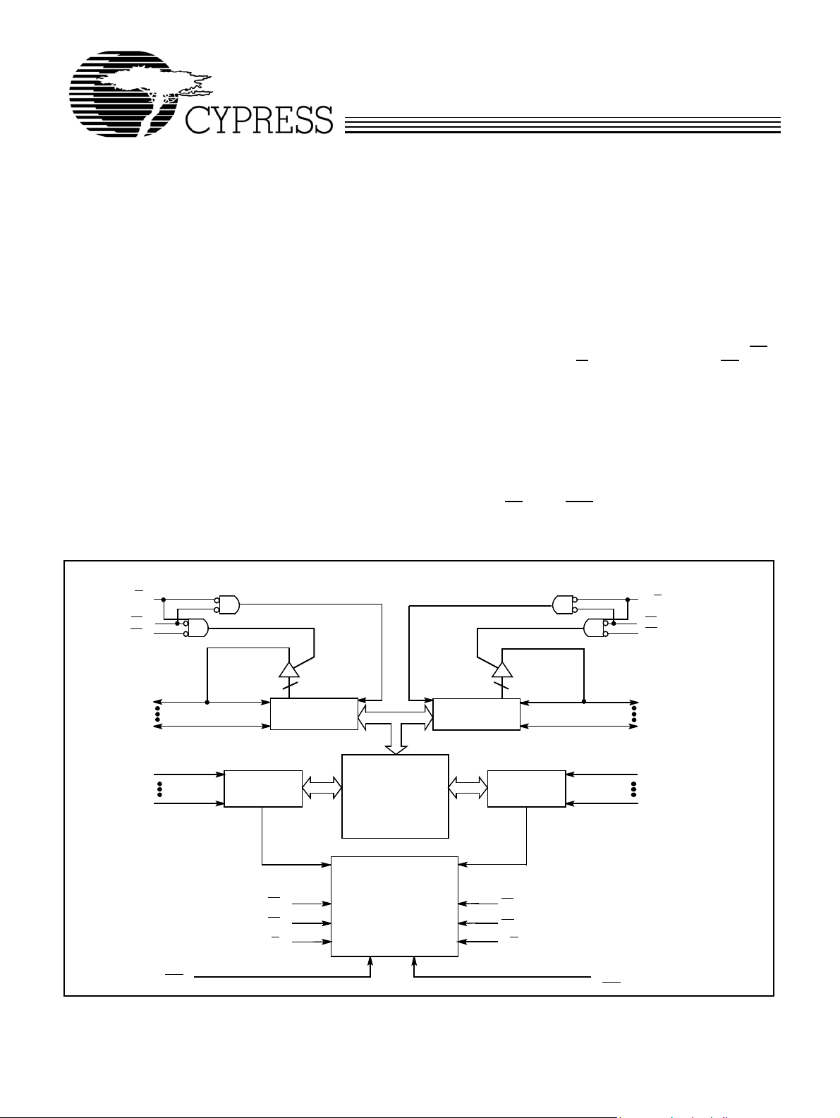
Logic Block Diagram
R/W
L
CE
L
OE
L
SRAM with Sema
hores
Functional Description
The CY7C135 and CY7C1342 are high-speed CMOS 4K x 8
dual-port static RAMs. The CY7C1342 includes semaphores
that provide a means to allocate portions of the dual-port RAM
or any shared resource. Two ports are provided permitting in
dependent, asynchronous access for reads and writes to any
location in memory. Application areas include interproces
sor/multiprocessor designs, communications status buffering,
and dual-port video/graphics memory.
Each port has independent control pins: chip enable (CE),
read or write enable (R/
CY7C135 is suited for those systems that do not require
on-chip arbitration or are intolerant of wait states. Therefore,
the user must be aware that simultaneous access to a location
is possible. Semaphores are offered on the CY7C1342 to as
sist in arbitrating between ports. The semaphore logic is comprised of eight shared latches. Only one side can control the
latch (semaphore) at any time. Control of a semaphore in di
cates that a shared resource is in use. An automatic power-down feature is controlled independently on each port by a
chip enable (
CE) pin or SEM pin (CY7C1342 only).
The CY7C135 and CY7C1342 are available in 52-pin PLCC.
W), and output enable (OE). The
R/W
R
CE
R
OE
R
-
-
-
-
I/O
7L
I/O
0L
A
11L
A
0L
(7C1342 only)
SEM
I/O
CONTROL
ADDRESS
DECODER
CE
L
OE
L
R/W
L
L
MEMORY
ARRAY
SEMAPHORE
ARBITRATION
(7C1342 only)
I/O
CONTROL
ADDRESS
DECODER
CE
R
OE
R
R/W
R
(7C1342 only)
SEM
I/O
7R
I/O
0R
A
11R
A
0R
R
1342–1
Cypress Semiconductor Corporation • 3901 North First Street • San Jose • CA 95134 • 408-943-2600
Document #: 38-06038 Rev. *B Revised June 22, 2004
CY7C135
CY7C1342
Selection Guide
7C135–15
7C1342–15
Maximum Access Time (ns) 15 20 25 35 55
Maximum Operating
Commercial 220 190 180 160 160
Current (mA)
Maximum St andby
Current for I
SB1
(mA)
Commercial 60 50 40 30 30
Pin Configurations
PLCC
Top View
L
0L
10L
11L
N/C
OE
A
A
A
A
A
A
A
A
A
A
A
A
I/O
I/O
I/O
I/O
A
A
A
A
A
A
A
A
A
I/O
I/O
I/O
I/O
7 6 5 4 3 2 52 51 50 49 48 47
1L
8
2L
9
3L
10
4L
11
5L
12
6L
13
7L
14
8L
15
9L
16
0L
17
1L
18
2L
19
3L
20
2122 23 24 25 26 27 28 29 30 31 32 33
4L5L6L
I/O
I/O
L
0L
OE
A
765432 525150494847
1L
8
2L
9
3L
10
4L
11
5L
12
6L
13
7L
14
8L
15
9L
16
0L
17
1L
18
2L
19
3L
20
2122 23 24 25 26 27 28 29 30 31 32 33
4L5L6L
I/O
I/O
A
I/O
I/O
10L
I/O
A
I/O
7C135
7L
NC
PLCC
Top View
L
11L
SEM
7C1342
7L
NC
GND
Pin Definitions
Left Port Right Port Description
A
0L–11L
CE
L
OE
L
R/W
L
SEM
L
(CY7C1342 only)
A
0R–11R
CE
R
OE
R
R/W
R
SEM
R
(CY7C1342 only)
Address Lines
Chip Enable
Output Enable
Read/Write Enable
Semaphore Enable. When asserted LOW, allows access to eight semaphores. The
three least significant bits of the address lines will determine which semaphore to write
or read. The I/O
by writing a 0 into the respective location.
pin is used when writing to a semaphore. Semaphores are requested
0
7C135–20
7C1342–20
L
R/W
1
GND
L
R/W
1
I/O
CE
I/O
R
LCER
CC
V
CE
R/W
0R1R2R3R4R5R6R
I/O
I/O
I/O
I/O
R
LCER
CC
V
R/W
0R1R2R3R4R5R6R
I/O
I/O
I/O
I/O
7C135–25
7C1342–25
10R
11R
N/C
A
A
OE
46
R
A
45
0R
A
44
1R
A
43
2R
A
42
3R
A
41
4R
A
40
5R
A
39
6R
A
38
7R
A
37
8R
A
36
9R
NC
35
I/O
34
7R
I/O
I/O
R
11R
SEM
A
I/O
I/O
1342–3
10R
A
OE
46
R
A
45
0R
A
44
1R
A
43
2R
A
42
3R
A
41
4R
A
40
5R
A
39
6R
A
38
7R
A
37
8R
A
36
9R
NC
35
I/O
34
7R
1342–4
7C135–35
7C1342–35
7C135–55
7C1342–55
Document #: 38-06038 Rev. *B Page 2 of 12
CY7C135
CY7C1342
Maximum Ratings
[1]
Static Discharge Voltage...........................................> 2001V
(per MIL-STD-883, Method 3015)
Storage Temperature ..................................–65°C to +150°C
Ambient Temperature with
Power Applied..............................................–55°C to +125°C
Supply Voltage to Ground Potential
(Pin 48 to Pin 24)............................................–0.5V to +7.0V
DC Voltage Applied to Outputs
in High Z State................................................–0.5V to +7.0V
DC Input Voltage
[2]
.........................................–3.0V to +7.0V
Electrical Characteristics Over the Operating Range
Latch-Up Current....................................................> 200 mA
Operating Range
Range
Commercial 0°C to +70°C 5V ± 10%
Industrial –40°C to +85°C 5V ± 10%
[4]
7C135–15
7C1342–1
Ambient
Temperature V
7C135–20
7C1342–207C135–25
5
7C1342–25
Max.Min.Max
Parameter Description Test Conditions Min.
V
OH
V
OL
V
IH
V
IL
I
IX
I
OZ
I
CC
I
SB1
I
SB2
I
SB3
Ind. 30
Output HIGH Voltage VCC = Min., IOH = –4.0 mA 2.4 2.4 2.4 V
Output LOW Voltage VCC = Min., IOL = 4.0 mA 0.4 0.4 0.4 V
Input HIGH Volt age 2.2 2.2 2.2 V
Input LOW Volt age 0.8 0.8 0.8 V
Input Load Current GND ≤ VI ≤ V
CC
Output Leakage Current Outputs Disabled,
GND ≤ VO ≤ V
CC
Operating Current VCC = Max.,
I
= 0 mA
OUT
Standby Current
(Both Ports TTL Levels)
Standby Current
(One Port TTL Level)
Standby Current
(Both Ports CMOS Levels)
CEL and CER ≥ VIH,
f = f
CEL and CER ≥ VIH,
f = f
MAX
MAX
[5]
[5]
Both Ports CE and CER ≥
V
– 0.2V ,
CC
VIN ≥ VCC – 0.2V
or VIN ≤ 0.2V, f = 0
[5]
Com’l 220 190 180 mA
Ind. 190
Com’l 60 50 40 mA
Ind. 50
Com’l 130 120 110 mA
Ind. 120
Com’l 15 15 15 mA
–10 +10 –10 +10 –10 +10 µA
–10 +10 –10 +10 –10 +10 µA
. Min.
CC
Max.Uni
t
I
SB4
Notes:
1. The Voltage on any input or I/O pin cannot exceed the power pin during power-up.
2. Pulse width < 20 ns.
3. TA is the “instant on” case temper ature.
4. See the last page of this specification for Group A subgroup testing information.
5. f
MAX
Standby Current
(One Port CMOS Level)
= 1/tRC = All inputs cycling at f = 1/tRC (except output enable). f = 0 means no address o r control lines cha nge. This applies only to input s at CMOS level st andby I
One Port CEL or
CER ≥ VCC – 0.2V ,
VIN ≥VCC – 0.2V or VIN ≤ 0.2V,
Active Port Outputs, f =
[5]
f
MAX
Com’l 125 115 100 mA
Ind. 115
SB3
.
Document #: 38-06038 Rev. *B Page 3 of 12
CY7C135
CY7C1342
Electrical Characteristics Over the Operating Range
[4]
(continued)
7C135–35
7C1342–35
7C135–55
7C1342–55
Parameter Description Test Conditions Min. Max. Min. Max. Unit
V
V
V
V
I
IX
I
OZ
I
CC
I
SB1
I
SB2
I
SB3
I
SB4
OH
OL
IH
IL
Output HIGH Voltage VCC = Min., IOH = –4.0 mA 2.4 2.4 V
Output LOW Voltage VCC = Min., IOL = 4.0 mA 0.4 0.4 V
2.2 2.2 V
Input LOW Volt age 0.8 0.8 V
Input Load Current GND ≤ VI ≤ V
CC
Output Leakage Current Outputs Disabled, GND ≤ VO ≤ V
Operating Current VCC = Max., I
VCC = Max., I
Standby Current
CEL and CER ≥ VIH, f = f
(Both Ports TTL Levels)
Standby Current
CEL and CER ≥ VIH, f = f
(One Port TTL Level)
Standby Current
(Both Ports CMOS Levels)
Both Ports CE and CER ≥ VCC – 0.2V ,
VIN ≥ VCC – 0.2V
or VIN ≤ 0.2V , f = 0
Standby Current
(One Port CMOS Level)
One Port CEL or CER ≥ VCC – 0.2V ,
VIN ≥ VCC – 0.2V or VIN ≤ 0.2V ,
Active Port Outputs, f = f
= 0 mA Com’l 160 160 mA
OUT
= 0 mA Ind. 180 180
OUT
[5]
MAX
MAX
MAX
[5]
[5]
[5]
CC
Com’l 30 30 mA
Ind. 40 40
Com’l 100 100 mA
Ind. 110 110
Com’l 15 15 mA
Ind. 30 30
Com’l 90 90 mA
Ind. 100 100
–10 +10 –10 +10 µA
–10 +10 –10 +10 µA
Capacitance
[6]
Parameter Description Test Conditions Max. Unit
C
C
IN
OUT
Input Capacitanc e TA = 25°C, f = 1 MHz,
Output Capacitance 10 pF
VCC = 5.0V
AC Test Loads and Waveforms
5V
R1= 893Ω
OUTPUT
C=
30pF
(a) Normal Load (Load 1)
Note:
6. Tested initially and after any design or process changes that may affect these parameters.
R1= 347Ω
1342–5 1342–6 1342–7
3.0V
GND
OUTPUT
C=
(b) Thévenin Equivalent (Load 1)
10%
≤ 3ns
R
= 250Ω
TH
30pF
ALL INPUT PULSES
90%
V
TH
90%
=1.4V
10%
≤3
ns
10 pF
R
OUTPUT
C= 5pF
(c) Three-State Delay (Load 3)
1342–8
TH
= 250Ω
V
X
Document #: 38-06038 Rev. *B Page 4 of 12

CY7C135
CY7C1342
Switching Characteristics Over the Operating Range
7C135–15
7C1342–15
[7, 8]
7C1342–20
7C135–20
7C135–25
7C1342–25
7C135–35
7C1342–35
7C135–55
7C1342–55
Parameter Description Min. Max. Min. Max. Min. Max. Min. Max. Min. Max. Unit
READ CYCLE
t
RC
t
AA
t
OHA
t
ACE
t
DOE
t
LZOE
t
HZOE
t
LZCE
t
HZCE
t
PU
t
PD
[9,10,11]
[9,10,11]
[9,10,11]
[9,10,11]
[11]
[11]
Read Cycle Time 15 20 25 35 55 ns
Address to Data Valid 15 20 25 35 55 ns
Output Hold From
3 3 3 3 3 ns
Address Change
CE LOW to Data Valid 15 20 25 35 55 ns
OE LOW to Data Valid 10 13 15 20 25 ns
OE Low to Low Z 3 3 3 3 3 ns
OE HIGH to High Z 10 13 15 20 25 ns
CE LOW to Low Z 3 3 3 3 3 ns
CE HIGH to High Z 10 13 15 20 25 ns
CE LOW to Power Up 0 0 0 0 0 ns
CE HIGH to Power Down 15 20 25 35 55 ns
WRITE CYCLE
t
WC
t
SCE
t
AW
t
HA
t
SA
t
PWE
t
SD
t
HD
[10,11]
t
HZWE
[10,11]
t
LZWE
[12]
t
WDD
[12]
t
DDD
SEMAPHORE TIMING
t
SOP
t
SWRD
t
SPS
Notes:
7. See the last page of this specification for Group A subgroup testing information.
8. T est condition s assume signal transit ion time of 3 ns or less, timing refer ence levels of 1.5V, input pulse levels of 0 to 3.0V, and out put loading of th e specified
IOL/IOH and 30-pF load capacitance.
9. At any given temperature and voltage condition for any given device, t
10. Test conditions used are Load 3.
11. This parameter is guaranteed but not tested.
12. For information on port-to-port delay through RAM cells from writing port to reading port, refer to Read Timing with Port-to-Port Delay waveform.
13. Semaphore timing applies only to CY7C1342.
Write Cycle Time 15 20 25 35 55 ns
CE LOW to Write End 12 15 20 30 50 ns
Address Set-Up to Write End 12 15 20 30 50 ns
Address Hold from Write End 2 2 2 2 2 ns
Address Set-Up to Write Start 0 0 0 0 0 ns
Write Pulse Width 12 15 20 25 50 ns
Data Set-Up to Write End 10 13 15 15 25 ns
Data Hold from Write End 0 0 0 0 0 ns
R/W LOW to High Z 10 13 15 20 25 ns
R/W HIGH to Low Z 3 3 3 3 3 ns
Write Pulse to Data Delay 30 40 50 60 70 ns
Write Data Valid to Read
25 30 30 35 40 ns
Data Valid
[13]
SEM Flag Update Pulse
10 10 10 15 15 ns
(OE or SEM)
SEM Flag Write to Read Time 5 5 5 5 5 ns
SEM Flag Contention Window 5 5 5 5 5 ns
is less than t
HZCE
LZCE
and t
HZOE
is less than t
LZOE
.
Document #: 38-06038 Rev. *B Page 5 of 12

Switching Waveforms
OE
CC
ISB
[14,15]
[14,16]
t
PU
R
Read Cycle No. 1
ADDRESS
DATA OUT
Read Cycle No. 2
[13]
SEM
or CE
DATA OUT
I
Read Timing with Port-to-Port
ADDRESS
t
OHA
t
LZCE
[17]
t
LZOE
Either Port Address Access
t
RC
t
AA
Either Port CE/OE Access
t
ACE
t
DOE
t
wc
MATCH
DATA VALID
DATA VALIDPREVIOUS DATA VALID
t
HZOE
CY7C135
CY7C1342
t
HZCE
t
PD
1342–9
1342–10
t
R/W
R
DATA
INR
ADDRESS
DATA
Notes:
14. R/W is HIGH for read cycle.
15. Device is continuously selected, CE = VIL and OE = VIL.
16. Address valid prior to or coincident with CE transition LOW.
17. CEL = CER =LOW; R/WL = HIGH
L
OUTL
MATCH
PWE
t
SD
VALID
t
WDD
t
DDD
t
HD
VALID
1342–11
Document #: 38-06038 Rev. *B Page 6 of 12

Switching Waveforms (continued)
CY7C135
CY7C1342
Write Cycle No. 1: OE Three-States Data I/Os (Either Port)
ADDRESS
SEM
[13]
t
SCE
ORCE
t
AW
R/W
t
SA
DATA
IN
OE
t
DATA
HZOE
OUT
HIGH IMPEDANCE
Write Cycle No. 2:R/W Three-States Data I/Os (Either Port)
[18,19,20]
t
WC
t
PWE
[19, 21]
t
SD
DATA VALID
t
HA
t
HD
t
LZOE
1342–12
t
WC
ADDRESS
t
[13]
SEM
CE
OR
t
R/W
DATA
IN
DATA
OUT
Notes:
18. The internal write time of the memory is defined by the overlap of CE or SEM LOW and R/W LOW . Both signals must be LOW to initiate a write and either signal can
terminate a write by going HIGH. The data input set-up and hold timing should be referenced to the rising edge of the signal that terminates the write.
19. R/W must be HIGH during all a ddress transaction s.
20. If OE is LOW during a R/W controlled write cycle, the write pulse width must be the larger of t
bus for the required t
.
t
PWE
21. Data I/O pins enter high-impedance when OE is held LOW during write.
. If OE is HIGH during a R/W controlled write cycle (as in this exampl e), this requirement does not apply and the write pulse can be as short as the specified
SD
SA
SCE
t
AW
t
PWE
t
SD
DATAVALID
t
HZWE
HIGH IMPEDANCE
or (t
PWE
+ tSD) to allow the I/O drivers to turn off and data to be placed on the
HZWE
t
HA
t
LZWE
t
HD
1342–13
Document #: 38-06038 Rev. *B Page 7 of 12

Switching Waveforms (continued)
Semaphore Read After Write Timing, Either Side (CY7C1342 only)
A0–A
SEM
I/O
R/W
2
0
t
VALID ADDRESS VALID ADDRESS
t
AW
t
t
SCE
HA
t
SD
DATAINVALID
t
SA
t
PWE
HD
[22]
t
SOP
CY7C135
CY7C1342
OUT
t
VALID
OHA
t
AA
t
ACE
DATA
t
SWRD
OE
WRITE CYCLE READ CYCLE
Timing Diagram of Semaphore Contention (CY7C1342 only)
A0L–A
R/W
SEM
A0R–A
R/W
SEM
2L
L
L
2R
R
R
MATCH
t
SPS
MATCH
t
SOP
[23,24,25]
t
DOE
1342–14
1342–15
Notes:
22. CE = HIGH for the duration of the above timing (both write and read cycle).
23. I/O0R = I/O0L = LOW (request semaphore); CER = CEL = HIGH.
24. Semaphores are reset (available to both ports) at cycle start.
25. If t
is violated, it is guaranteed that only one side will gain access to the semaphore.
SPS
Document #: 38-06038 Rev. *B Page 8 of 12

CY7C135
CY7C1342
Architecture
The CY7C135 consists of an array of 4K words of 8 bits each
of dual-port RAM cells, I/O and address lines, and control sig
nals (CE, OE, R/W). Two semaphore control pins exist for the
CY7C1342 (
SEM
L/R
).
-
Functional Description
Write Operation
Data must be set up for a duration of tSD before the rising edge
of R/
W in order to guarantee a valid write. Since there is no
on-chip arbitration, the user must be sure that a specific loca
tion will not be accessed simultaneously by both ports or erroneous data could result. A write operation is controlled by either the OE pin (see Write Cycle No. 1 timing diagram) or the
W pin (see Write Cycle No. 2 timing diagram). Data can be
R/
written t
falling edge of R/
summarized in
after the OE is deasserted or t
HZOE
W. Required inputs for write operations are
Table 1.
HZWE
after the
If a location is being written to by one port and the opposite
port attempts to read the same location, a port-to-port
flowthrough delay is met before the data is valid on the output.
Data will be valid on the port wishing to read the location t
after the data is presented on the writing port.
Read Operation
When reading the device, the user must assert both the OE
and CE pins. Data will be available t
OE are asserted. If the user of the CY7C1342 wishes to ac-
after CE or t
ACE
DOE
cess a semaphore, the SEM pin must be asserted instead of
the
CE pin. Required inputs for read operations are summa-
rized in Table 1.
Semaphore Operation
The CY7C1342 provides eight semaphore latches which a re
separate from the dual port memory locations. Semaphores
are used to reserve resources which are shared between the
two ports. The state of the semaphore indicates that a re
source is in use. For example, if the left port wants to request
a given resource, it sets a latch by writing a zero to a sema
phore location. The left port then verifies its success in setting
the latch by reading it. After writing to the semaphore,
OE must be deasserted for t
semaphore. The semaphore value will be available t
after the rising edge of the semaphore write. If the left port
t
DOE
was successful (reads a zero), it assumes control over the
before attempting to read the
SOP
shared resource, otherwise (reads a one) it assumes the right
port has control and continues to poll the semaphore. Whe n
the right side has relinquished control of the sema phore (by
writing a one), the left side will succeed in gaining control of
the semaphore. If the left side no longer requires the sema
phore, a one is written to cancel its request.
Semaphores are accessed by asserting SEM LOW. The SEM
pin functions as a chip enable for the semaphore latches. CE
must remain HIGH during SEM LOW. A
semaphore address.
OE and R/W are used in the same man-
represents the
0–2
ner as a normal memory access. When writing or reading a
semaphore, the other address pins have no effect.
When writing to the semaphore, only I/O0 is used. If a 0 is
written to the left port of an unused semaphore, a one will
appear at the same semaphore address on the right port. That
semaphore can now only be modified by the side showing a
DDD
after
SEM or
+
SWRD
-
-
-
-
zero (the left port in this case). If the left port now relinquishes
control by writing a one to the semaphore, the semaphore will
be set to one for both sides. However, if the right port had
requested the semaphore (written a zero) while the left port
had control, the right port would immediately own the sema
phore. Table 2 shows sample semaphore operations.
When reading a semaphore, all eight data lines output the
semaphore value. The read value is latched in an output reg
ister to prevent the semaphore from changing state during a
write from the other port. If both ports request a semaphore
control by writing a 0 to a semaphore within t
it is guaranteed that only one side will gain access to the sema
of each other ,
SPS
phore.
Initialization of the semaphore is not automatic and must be
reset during initialization program at power-up. All sema
phores on both sides should have a one written into them at
initialization from both sides to assure that they will be free
when needed.
Table 1. Non-Contending Read/Write
Inputs Outputs
CE R/W OE SEM
I/O0 – I/O
7
Operation
H X X H High Z Power-Down
H H L L Data Out Read
Semaphore
X X H X High Z I/O Lines Disabled
H L X L Data In Write to Semaphore
L H L H Data Out Read
L L X H Data In Write
L X X L Illegal Condition
Table 2. Semaphore Operation Example
I/O
I/O
Function
Left
0-7
0-7
Right Status
No Action 1 1 Semaphore free
Left port writes
semaphore
Right port writes 0 to
semaphore
Left port writes 1 to
semaphore
0 1 Left port obtains
semaphore
0 1 Right side is denied
access
1 0 Right port is granted
access to Sema
-
phore
Left port writes 0 to
semaphore
Right port writes 1 to
semaphore
Left port writes 1 to
semaphore
Right port writes 0 to
semaphore
Right port writes 1 to
semaphore
Left port writes 0 to
semaphore
Left port writes 1 to
semaphore
1 0 No change. Left port
is denied access
0 1 Left port obtains
semaphore
1 1 No port accessing
semaphore address
1 0 Right port obtains
semaphore
1 1 No port accessing
semaphore
0 1 Left port obtains
semaphore
1 1 No port accessing
semaphore
-
-
-
-
Document #: 38-06038 Rev. *B Page 9 of 12

Typical DC and AC Characteristics
NORMALIZED SUPPLY CURRENT
OUTPUT SOURCE CURRENT
CY7C135
CY7C1342
NORMALIZED SUPPLY CURRENT
vs. SUPPLY VOLTAGE
1.4
I
SB
SB
1.2
CC
1.0
0.8
0.6
0.4
NORMALIZED I, I
0.2
0.0
I
CC
4.0 4.5 5.0 5.5
SUPPLY VOLTAGE (V)
NORMALIZED ACCESS TIME
vs. SUPPLY VOLTAGE
1.10
=25°C
T
AA
A
1.05
1.00
NORMALIZED t
0.95
4.0 4.5 5.0 5.5 6.0
SUPPLY VOLTAGE (V)
vs. AMBIENT TEMPERATURE
1.2
I
CC
1.0
CC SB
0.8
0.6
0.4
NORMALIZED I, I
6.0
0.2
0.6
–55 25 125
I
SB3
V
CC
V
IN
AMBIENT TEMPERATURE (°C)
NORMALIZED ACCESS TIME
vs. AMBIENT TEMPERATURE
1.2
AA
1.1
1.0
V
NORMALIZED t
CC
0.9
0.8
–55 125
25
AMBIENT TEMPERATURE (°C)
=5.0V
= 5.0V
= 5.0V
vs. OUTPUT VOLTAGE
140
120
100
80
60
40
20
0
OUTPUT SOURCE CURRENT (mA)
0 1.0 2.0 3.0 5.0
OUTPUT VOLTAGE (V)
OUTPUT SINK CURRENT
vs. OUTPUT VOLTAGE
100
90
80
70
V
60
OUTPUT SINK CURRENT (mA)
50
CC
T
A
0.0 1.0 2.0 3.0
OUTPUT VOLTAGE (V)
V
CC
T
A
=5.0V
= 25°C
=5.0V
=25°C
4.0
4.0
5.0
TYPICAL POWER-ON CURRENT
vs. SUPPLY VOLTAGE
1.0
PC
0.75
0.50
NORMALIZED t
0.25
0.0
0 1.0 2.0 3.0 5.0
SUPPLY VOLTAGE (V)
4.0
TYPICAL ACCESS TIME CHANGE
vs. OUTPUT LOADING
20.0
15.0
AA
10.0
DELTA t (ns)
5.0
V
T
CC
= 25°C
A
0
0 200 400 600 800
CAPACITANCE (pF)
=4.5V
1000
NORMALIZED I
1.25
V
T
CC
V
=5.0V
CC
=25°C
A
= 0.5V
IN
vs.CYCLE TIME
CC
1.0
0.75
NORMALIZED I
0.50
10 50
20 30
CYCLE FREQUENCY (MHz)
40
Document #: 38-06038 Rev. *B Page 10 of 12

CY7C135
CY7C1342
Ordering Information
4K x8 Dual-Port SRAM
Speed
(ns) Ordering Code
15 CY7C135–15JC J69 52-Lead Plastic Leaded Chip Carrier Commercial
20 CY7C135–20JC J69 52-Lead Plastic Leaded Chip Carrier Commercial
25 CY7C135–25JC J69 52-Lead Plastic Leaded Chip Carrier Commercial
CY7C135–25JI J69 52-Lead Plastic Leaded Chip Carrier Industrial
35 CY7C135–35JC J69 52-Lead Plastic Leaded Chip Carrier Commercial
CY7C135–35JI J69 52-Lead Plastic Leaded Chip Carrier Industrial
55 CY7C135–55JC J69 52-Lead Plastic Leaded Chip Carrier Commercial
CY7C135–55JI J69 52-Lead Plastic Leaded Chip Carrier Industrial
4K x8 Dual-Port SRAM with Semaphores
Speed
(ns) Ordering Code
15 CY7C1342–15JC J69 52-Lead Plastic Leaded Chip Carrier Commercial
20 CY7C1342–20JC J69 52-Lead Plastic Leaded Chip Carrier Commercial
25 CY7C1342–25JC J69 52-Lead Plastic Leaded Chip Carrier Commercial
CY7C1342–25JI J69 52-Lead Plastic Leaded Chip Carrier Industrial
35 CY7C1342–35JC J69 52-Lead Plastic Leaded Chip Carrier Commercial
CY7C1342–35JI J69 52-Lead Plastic Leaded Chip Carrier Industrial
55 CY7C1342–55JC J69 52-Lead Plastic Leaded Chip Carrier Commercial
CY7C1342–55JI J69 52-Lead Plastic Leaded Chip Carrier Industrial
Package
Name Package Type
Package
Type Package Type
Operating
Range
Operating
Range
Package Diagrams
52-Lead Plastic Leaded Chip Carrier J69
51-85004-*A
Document #: 38-06038 Rev. *B Page 11 of 12
© Cypress Semiconductor Corporation, 2004. The information contained herein is subject to ch an ge without notice. Cypress Semiconductor Corporation assu me s no r esp onsib i lity f or th e u se
of any circuitry other than circuitry embodied in a Cypress product. Nor does it convey or imply any license under patent or other rights. Cypress products are not warranted nor intended to be
used for medical, life support, life saving, critical control or safety applications, unless pursuant to an express written agreement with Cypress. Furthermore, Cypress does not authorize its
products for use as critical components in life-support systems where a malfunction or failure may reasonably be expected to result in significant injury to the user. The inclusion of Cypress
products in life-support systems application implies that the manufacturer assumes all risk of such use and in doing so indemnifies Cypress against all charges.

CY7C135
CY7C1342
Document History Page
Document Title: CY7C135/CY7C1342 4K x 8 Dual Port Static RAM and 4K x 8 Dual Port Static RAM w/Semaphores
Document Number: 38-06038
REV. ECN NO.
** 110181 10/21/01 SZV Change from Spec number: 38-00541 to 38-06038
*A 122288 12/27/02 RBI Power up requirements added to Maximum Ratings Information
*B 236763 SEE ECN YDT Removed cross information from features section
Issue
Date
Orig. of
Change Description of Change
Document #: 38-06038 Rev. *B Page 12 of 12
 Loading...