

Page 1
CY7C1347G
4-Mbit (128K x 36) Pipelined Sync SRAM
Features
Note
1. For best practice recommendations, refer to the Cypress application note AN1064, SRAM System Guidelines.
■ Fully registered inputs and outputs for pipelined operation
■ 128K x 36 common IO architecture
■ 3.3V core power supply (V
■ 2.5V/3.3V IO power supply (V
■ Fast clock to output times: 2.6 ns (for 250 MHz device)
■ User-selectable burst counter supporting Intel
interleaved or linear burst sequences
■ Separate processor and controller address strobes
■ Synchronous self-timed writes
■ Asynchronous output enable
■ Offered in Pb-free 100-Pin TQFP, Pb-free and non Pb-free
119-Ball BGA package, and 165-Ball FBGA package
■ “ZZ” sleep mode option and stop clock option
■ Available in industrial and commercial temperature ranges
DD
)
DDQ
)
®
Pentium
®
Functional Description
[1]
The CY7C1347G is a 3.3V, 128K x 36 synchronous-pipelined
SRAM designed to support zero-wait-state secondary cache
with minimal glue logic. CY7C1347G IO pins can operate at
either the 2.5V or the 3.3V level. The IO pins are 3.3V tolerant
when V
registers controlled by the rising edge of the clock. All data
= 2.5V. All synchronous inputs pass through input
DDQ
outputs pass through output registers controlled by the rising
edge of the clock. Maximum access delay from the clock rise is
2.6 ns (250 MHz device). CY7C1347G supports either the
interleaved burst sequence used by the Intel Pentium processor
or a linear burst sequence used by processors such as the
PowerPC
®
. The burst sequence is selected through the MODE
pin. Accesses can be initiated by asserting either the Address
Strobe from Processor (ADSP) or the Address Strobe from
Controller (ADSC
the burst sequence is controlled by the ADV
) at clock rise. Address advancement through
input. A 2-bit on-chip
wraparound burst counter captures the first address in a burst
sequence and automatically increments the address for the rest
of the burst access.
Byte write operations are qualified with the four Byte Write Select
(BW
write inputs and writes data to all four bytes. All writes are
) inputs. A Global Write Enable (GW) overrides all byte
[A:D]
conducted with on-chip synchronous self-timed write circuitry.
Three synchronous Chip Selects (CE
asynchronous Output Enable (OE
, CE2, CE3) and an
1
) provide for easy bank
selection and output tri-state control. To provide proper data
during depth expansion, OE is masked during the first clock of a
read cycle when emerging from a deselect ed state.
Selection Guide
Specification 250 MHz 200 MHz 166 MHz 133 MHz Unit
Maximum Access Time 2.6 2.8 3.5
Maximum Operating Current 325 265 240
Maximum CMOS Standby Cur rent 40 40 40 40 mA
Cypress Semiconductor Corporation • 198 Champion Court • San Jose, CA 95134-1709 • 408-943-2600
Document #: 38-05516 Rev. *F Revised January 15, 2009
4.0 ns
225 mA
[+] Feedback
Page 2
CY7C1347G
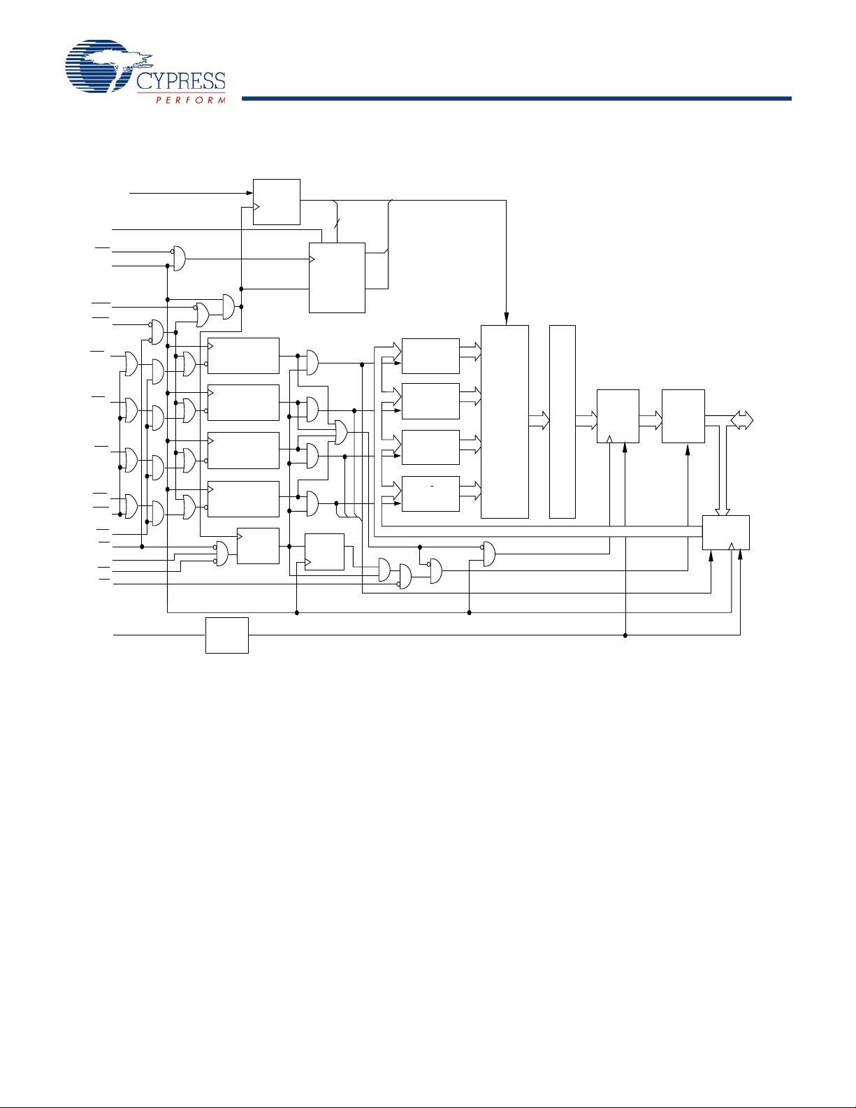
Block Diagram
ADDRESS
REGISTER
ADV
CLK
BURST
COUNTER
AND
LOGIC
CLR
Q1
Q0
ADSP
ADSC
MODE
BWE
GW
CE
1
CE
2
CE
3
OE
ENABLE
REGISTER
OUTPUT
REGISTERS
SENSE
AMPS
OUTPUT
BUFFERS
E
PIPELINED
ENABLE
INPUT
REGISTERS
A 0, A1, A
BW
B
BW
C
BW
D
BW
A
MEMORY
ARRAY
DQs
DQP
A
DQP
B
DQP
C
DQP
D
SLEEP
CONTROL
ZZ
A
[1:0]
2
DQA,DQP
A
BYTE
WRITE REGISTER
DQ
B,
DQP
B
BYTE
WRITE REGISTER
DQ
C,
DQP
C
BYTE
WRITE REGISTER
DQ
D,
DQP
D
BYTE
WRITE REGISTER
DQ
A,
DQP
A
BYTE
WRITE DRIVER
DQ
B,
DQP
B
BYTE
WRITE DRIVER
DQ
C,
DQP
C
BYTE
WRITE DRIVER
DQ
D
,DQP
D
BYTE
WRITE DRIVER
Document #: 38-05516 Rev. *F Page 2 of 22
[+] Feedback
Page 3
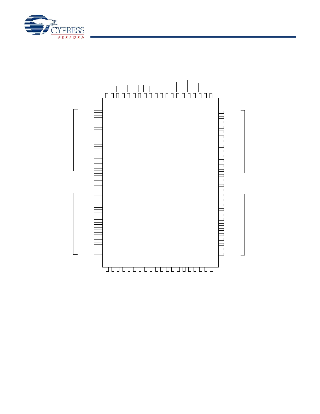
CY7C1347G
Pinouts
AAAAA1A
0
NC/72M
NC/36M
V
SS
V
DD
NC/18M
NC/9M
AAAAAAA
DQP
B
DQ
B
DQ
B
V
DDQ
V
SSQ
DQ
B
DQ
B
DQ
B
DQ
B
V
SSQ
V
DDQ
DQ
B
DQ
B
V
SS
NC
V
DD
ZZ
DQ
A
DQ
A
V
DDQ
V
SSQ
DQ
A
DQ
A
DQ
A
DQ
A
V
SSQ
V
DDQ
DQ
A
DQ
A
DQP
A
DQP
C
DQ
C
DQ
C
V
DDQ
V
SSQ
DQ
C
DQ
C
DQ
C
DQ
C
V
SSQ
V
DDQ
DQ
C
DQ
C
NC
V
DD
NC
V
SS
DQ
D
DQ
D
V
DDQ
V
SSQ
DQ
D
DQ
D
DQ
D
DQ
D
V
SSQ
V
DDQ
DQ
D
DQ
D
DQP
D
AACE1CE2BWDBWCBWBBWACE3VDDVSSCLKGWBWEOEADSC
ADSP
ADVAA
1
2
3
4
5
6
7
8
9
10
11
12
13
14
15
16
17
18
19
20
21
22
23
24
25
26
27
28
29
30
31323334353637383940414243444546474849
50
80
79
78
77
76
75
74
73
72
71
70
69
68
67
66
65
64
63
62
61
60
59
58
57
56
55
54
53
52
51
100999897969594939291908988878685848382
81
MODE
BYTE A
BYTE B
BYTE D
BYTE C
CY7C1347G
Figure 1. 100-Pin TQFP
Document #: 38-05516 Rev. *F Page 3 of 22
[+] Feedback
Page 4
CY7C1347G
Pinouts (continued)
2
345671
A
B
C
D
E
F
G
H
J
K
L
M
N
P
R
T
U
V
DDQ
NC/288M
NC/144M
DQP
C
DQ
C
DQ
D
DQ
C
DQ
D
AA AAADSP V
DDQ
CE
2
A
DQ
C
V
DDQ
DQ
C
V
DDQ
V
DDQ
V
DDQ
DQ
D
DQ
D
NC
NC
V
DDQ
V
DD
CLK
V
DD
V
SS
V
SS
V
SS
V
SS
V
SS
V
SS
V
SS
V
SS
NC/576M
NC/1G
NC
NC
NCNCNCNC
NC/36MNC/72M
NC
V
DDQ
V
DDQ
V
DDQ
AAA
A
CE
3
AA
A
AA
A
A0
A1
DQ
A
DQ
C
DQ
A
DQ
A
DQ
A
DQ
B
DQ
B
DQ
B
DQ
B
DQ
B
DQ
B
DQ
B
DQ
A
DQ
A
DQ
A
DQ
A
DQ
B
V
DD
DQ
C
DQ
C
DQ
C
V
DD
DQ
D
DQ
D
DQ
D
DQ
D
ADSC
NC
CE
1
OE
ADV
GW
V
SS
V
SS
V
SS
V
SS
V
SS
V
SS
V
SS
V
SS
DQP
A
MODE
DQP
D
DQP
B
BW
B
BW
C
NC V
DD
NC
BW
A
NC
BWE
BW
D
ZZ
A
Figure 2. 119-Ball BGA
2345671
A
B
C
D
E
F
G
H
J
K
L
M
N
P
R
NC
NC/288M
NC/144M
DQP
C
DQ
C
DQP
D
NC
DQ
D
CE1BW
B
CE
3
BW
C
BWE
A
CE2
DQ
C
DQ
D
DQ
D
MODE
NC
DQ
C
DQ
C
DQ
D
DQ
D
DQ
D
NC/36M
NC/72M
V
DDQ
BW
D
BW
A
CLK
GW
V
SS
V
SS
V
SS
V
SS
V
DDQ
V
SS
V
DD
V
SS
V
SS
V
SS
NC/18M
V
SS
V
SS
V
SS
V
DDQ
V
DDQ
NC
V
DDQ
V
DDQ
V
DDQ
V
DDQ
A
A
V
DD
V
SS
V
DD
V
SS
V
SS
V
DDQ
V
DD
V
SS
V
DD
V
SS
V
DD
V
SS
V
SS
V
SS
V
DD
V
DD
V
SS
V
DD
V
SS
V
SS
NC
NC
V
SS
NC
A
A
DQ
C
V
SS
DQ
C
V
SS
DQ
C
DQ
C
V
SS
V
SS
V
SS
V
SS
V
SS
V
SS
V
SS
A1
DQ
D
DQ
D
NC
NC
V
DDQ
V
SS
NC
891011
NC/9M
ADV
A
ADSC
NC
OE ADSP
A
NC/576M
V
SS
V
DDQ
NC/1G DQP
B
V
DDQ
V
DD
DQ
B
DQ
B
DQ
B
NC
DQ
B
NC
DQ
A
DQ
A
V
DD
V
DDQ
V
DD
V
DDQ
DQ
B
V
DD
NC
V
DD
DQ
A
V
DD
V
DDQ
DQ
A
V
DDQ
V
DD
V
DD
V
DDQ
V
DD
V
DDQ
DQ
A
V
DDQ
AA
V
SS
A
A
A
DQ
B
DQ
B
DQ
B
ZZ
DQ
A
DQ
A
DQP
A
DQ
A
A
V
DDQ
A
A0
A
V
SS
Figure 3. 165-Ball FBGA
Document #: 38-05516 Rev. *F Page 4 of 22
[+] Feedback
Page 5
CY7C1347G
Table 1. Pin Definitions
Name IO Description
A0,A1,A Input-
Synchronous
BWA,BW
BWC,BW
B,
D
InputSynchronous
GW Input-
Synchronous
BWE Input-
Synchronous
Address Inputs Used to Select One of the 128K Address Locations. Sampled at the rising edge
of the CLK if ADSP
the 2-bit counter.
or ADSC is active LOW, and CE1, CE2, and CE3 are sampled active. A
[1:0]
feeds
Byte Write Select Inputs, Active LOW. Qualified with BWE to conduct byte writes to the SRAM.
Sampled on the rising edge of CLK.
Global Write Enable Input, Active LOW. When asserted LOW on the rising edge of CLK, a global
write is conducted (ALL bytes are written, regardless of the values on BW
and BWE).
[A:D]
Byte Write Enable Input, Active LOW. Sampled on the rising edge of CLK. This signal must be
asserted LOW to conduct a byt e wri te .
CLK Input-Clock Clock Input. Used to capture all synchronous inputs to the device. Also used to increment the burst
CE
CE
CE
1
2
3
InputSynchronous
InputSynchronous
InputSynchronous
OE Input-
Asynchronous
ADV Input-
Synchronous
ADSP Input-
Synchronous
ADSC Input-
Synchronous
ZZ Input-
Asynchronous
counter when ADV
Chip Enable 1 Input, Active LOW. Sampled on the risin g edge of CLK. Used in conjunction with CE2
and CE
a new external address is loaded.
to select or deselect the device. ADSP is ignore d if CE1 is HIGH. CE1 is sampled only when
3
Chip Enable 2 Input, Active HIGH. Sampled on the risi ng edge of CLK. Used in conj unction with CE1
and CE
to select or deselect the device. CE2 is sampled only when a new external address is loaded.
3
Chip Enable 3 Input, Active LOW. Sampled on th e rising edge of CL K. Used in conjunctio n with CE
and CE2 to select or deselect the device. CE3 is sampled only when a new external address is l oaded.
Output Enable, Asynchronous Input, Active LOW. Controls the direction of the IO pins. When LOW ,
the IO pins behave as outputs. When deasserted HIGH, IO pins are tri-stated, and act as input data
pins. OE
is masked during the first clock of a read cycle when emerging from a deselected state.
Advance Input Signal, Sampled on the Rising Edge of CLK. When asserted, it automatically
increments the address in a burst cycle.
Address Strobe from Processor, Sampled on the Rising Edge of CLK. When asserted LOW,
addresses presented to the device are captured in the address registers. A
burst counter. When ADSP
when CE
is deasserted HIGH.
1
Address Strobe from Controller, Sampled on the Rising Edge of CLK. When asserted LOW,
addresses presented to the device are captured in the address registers. A
burst counter. When ADSP
ZZ “Sleep” Input. This active HIGH input places the device in a non-time-critical “sleep” condition with
data integrity preserved. During normal operat ion, this pin must be LOW o r lef t floating. ZZ p in has an
is asserted LOW, during a burst operation.
and ADSC are both asserted, only ADSP is recognized. ASDP is ignored
and ADSC are both asserted, onl y AD SP is recognized.
are also loaded into the
[1:0]
are also loaded into the
[1:0]
internal pull down.
DQ
DQ
DQP
DQP
A, DQB
C, DQD
DQP
A,
DQP
C,
IOSynchronous
B,
D
Bidirectional Data IO Lines. As inputs, they feed into an on-chip data register that is t riggered by the
rising edge of CLK. As outputs , they deliver the dat a contained in the memory location spec ified by the
addresses presented during the previous clock rise of the read cycle. The direction of the pins is
controlled by OE
. When OE is asserted LOW, the pins behave as outputs. When HIGH, DQs and DQPs
are placed in a tri-state condition.
V
DD
V
SS
V
DDQ
V
SSQ
MODE Input-
Power Supply Power Supply Inputs to the Core of the Device
Ground Ground for the Core of the Device
IO Power Supply Power Supply for the IO circuitry
IO Ground Ground for the IO circuitry
Selects Burst Order. When tied to GND selects linear burst sequence. When tied to V
Static
floating selects interleaved burst sequence. This is a strap pin and must remain static during device
DDQ
or left
operation. Mode pin has an internal pull up.
NC, NC/9M,
NC/18M,
NC/36M,
– No Connects. Not internally connected to the die. NC/9M, NC/18M, NC/36M, NC/72M, NC/144M,
NC/288M, NC/576M, and NC/1G are address expansion pins that are not int ernall y conn ected to the
die.
NC/72M,
NC/144M,
NC/288M,
NC/576M,
NC/1G
1
Document #: 38-05516 Rev. *F Page 5 of 22
[+] Feedback
Page 6

CY7C1347G
Functional Overview
All synchronous inputs pass through input registers controlled by
the rising edge of the clock. All data outputs pass through output
registers controlled by the rising edge of the clock. Maximum
access delay from the clock rise (t
The CY7C1347G supports secondary cache in systems using
either a linear or interleaved burst sequence. The linear burst
sequence is suited for processors that use a linear burst
sequence. The burst order is user selectable, and is determined
by sampling the MODE input. Accesses can be initiated with
either the Address S trobe from Processor (ADSP
Strobe from Controller (ADSC
the burst sequence is controlled by the ADV
on-chip wraparound burst counter captures the first address in a
burst sequence and automatically increments the address for the
rest of the burst access.
Byte write operations are qualified with the Byte Write Enable
(BWE
) and Byte Write Select (BW
Enable (GW
) overrides all byte write inputs and writes data to all
four bytes. All writes are simplified with on-chip synchronous
self-timed write circuitry.
Three synchronous Chip Selects (CE
asynchronous Output Enable (OE
selection and output tri-state control. ADSP
HIGH.
Single Read Accesses
This access is initiated when the following conditions are
satisfied at clock rise: (1) ADSP
, CE2, CE3 are all asserted active, and (3) the write signals
CE
1
(GW
, BWE) are all deasserted HIGH. ADSP is ignored if CE1 is
HIGH. The address presented to the address inputs (A
stored into the address advancement logic and the Address
Register while being presented to the memory core. The corresponding data is allowed to propagate to the input of the Output
Registers. At the rising edge of the next clock the data is allowed
to propagate through the Output Register and onto the data bus
within 2.6 ns (250 MHz device) if OE
exception occurs when the SRAM is emerging from a deselected
state to a selected state, its outputs are always tri-stated during
the first cycle of the access. After the first cycle of the access,
the outputs are controlled by the OE
read cycles are supported. After the SRAM is deselected at clock
rise by the chip select and either ADSP
output tri-states immediately.
Single Write Accesses Initiated by ADSP
This access is initiated when both of the following conditions are
satisfied at clock rise: (1) ADSP
CE
, CE3 are all asserted active. The address presented to
2
is loaded into the Address Register and the address
A
[16:0]
advancement logic while being delivered to the RAM core. The
write signals (GW
ignored during this first cycle.
ADSP
-triggered write accesses require two clock cycles to
complete. If GW
data presented to the DQs and DQPs inputs is written into the
corresponding address location in the RAM core. If GW
then the write operation is controlled by BWE
signals. The CY7C1347G provides byte write capability that is
, BWE, and BW
is asserted LOW on the second clock rise, the
) is 2.6 ns (250 MHz device).
CO
) or the Address
). Address advancement through
input. A two-bit
) inputs. A Global Write
[A:D]
, CE2, CE3) and an
1
) provide for easy bank
is ignored if CE1 is
or ADSC is asserted LOW, (2)
) is
[16:0]
is active LOW. The only
signal. Consecutive single
or ADSC signals, its
is asserted LOW, and (2) CE1,
) and ADV inputs are
[A:D]
is HIGH,
and BW
[A:D]
described in Table 6 on page 8. Asserting the Byte Write Enable
input (BWE
) with the selected Byte Write (BW
tively writes to only the desired bytes.
) input selec-
[A:D]
Bytes not selected during a byte write operation remain
unaltered. A synchronous self-timed write mechanism is
provided to simplify the write operations.
Because the CY7C1347G is a common IO device, the Output
Enable (OE
) must be deasserted HIGH before presenting data
to the DQs and DQPs inputs. Doing so tri-states the output
drivers. As a safety precaution, DQs and DQPs are automatically
tri-stated whenever a write cycle is detected, regardless of the
state of OE
.
Single Write Accesse s Initiated by ADSC
ADSC write accesses are initiated when the following conditions
are satisfied: (1) ADSC
HIGH, (3) CE
appropriate combination of the write inputs (GW
BW
[A:D]
byte(s). ADSC
, CE2, CE3 are all asserted active, and (4) the
1
) are asserted active to conduct a write to the desired
-triggered write accesses require a single clock
cycle to complete. The address presented to A
the address register and the address advancement logic while
being delivered to the RAM core. The ADV input is ignored
during this cycle. If a global write is conducted, the data
presented to the DQs and DQPs is written into the corresponding
address location in the RAM core. If a byte write is conducted,
only the selected bytes are written. Bytes not selected during a
byte write operation remain unaltered. A synchronous self-timed
write mechanism has been provided to simplify the write ope rations.
Because the CY7C1347G is a common IO device, the Output
Enable (OE
) must be deasserted HIGH before presenting data
to the DQs and DQPs inputs. Doing so tri-states the output
drivers. As a safety precaution, DQs and DQPs are automatically
tri-stated whenever a write cycle is detected, regardless of the
state of OE.
is asserted LOW , (2) ADSP is deasserted
, BWE, and
is loaded into
[16:0]
Burst Sequences
The CY7C1347G provides a two-bit wraparound counter, fed by
A
, that implements either an interleaved or linear burst
[1:0]
sequence. The interleaved burst sequence is designed
specifically to support Intel Pentium applications. The linear
burst sequence is designed to support processors tha t follow a
linear burst sequence. The burst sequence is user-selectable
through the MODE input.
Asserting ADV
LOW at clock rise automatically increments the
burst counter to the next address in the burst sequence. Both
read and write burst operations are supported.
Sleep Mode
The ZZ input pin is an asynchronous input. Asserting ZZ places
the SRAM in a power conservation “sleep” mode. Two clock
cycles are required to enter into or exit from this “sleep” mode.
While in this mode, data integrity is guaranteed. Accesses
pending when entering the “sleep” mode are not considered valid
nor is the completion of the operation guaranteed. The device
must be deselected before entering the “sleep” mode. CE
CE
, ADSP, and ADSC must remain inactive for the duration of
3
t
after the ZZ input returns LOW.
ZZREC
, CE2,
1
Document #: 38-05516 Rev. *F Page 6 of 22
[+] Feedback
Page 7
CY7C1347G
Table 2. Interleaved Burst Sequence
Note
2. X = “Do Not Care.” H = Logic HIGH, L = Logic LOW.
3. WRITE
= L when any one or more Byte Write Enable signals (BWA, BWB, BWC, BWD) and BWE = L or GW = L. WRITE = H when all Byte Write Enable signals (BWA,
BW
B
, BWC, BWD), BWE, GW = H.
4. The DQ pins are controlled by the current cycle and the OE
signal. OE is asynchronous and is not sampled with the clock.
5. The SRAM always initiates a read cycle when ADSP
is asserted, regardless of the state of GW, BWE, or BW
[A:D]
. Writes may occur only on subsequent clocks after
the ADSP
or with the assertion of ADSC. As a result, OE must be driven HIGH before the start of the write cycle to allow th e outputs to tri -state. OE is a don't care for
the remainder of the write cycle.
6. OE
is asynchronous and is not sampled with the clock rise. It is masked internally during write cycles. During a read cycle all data bits are tri-state when OE is inactive
or when the device is deselected, and all data bits behave as output when OE
is active (LOW).
Address
A
[1:0]
First
Second
Address
A
[1:0]
Address
A
[1:0]
Third
00 01 10 11
01 00 11 10
10 11 00 01
11 10 01 00
Fourth
Address
A
[1:0]
Table 3. Linear Burst Sequence
Address
A
[1:0]
First
Second
Address
A
[1:0]
Address
A
[1:0]
Third
00 01 10 11
01 10 11 00
10 11 00 01
11 00 01 10
Fourth
Address
A
[1:0]
Table 4. ZZ Mode Electrical Characteristics
Parameter Description Test Conditions Min Max Unit
I
DDZZ
t
ZZS
t
ZZREC
t
ZZI
t
RZZI
Table 5. Truth Table
Snooze mode standby current ZZ > VDD − 0.2V 40 mA
Device operation to ZZ ZZ > VDD − 0.2V 2t
ZZ recovery time ZZ < 0.2V 2t
CYC
ZZ Active to snooze current This parameter is sampled 2t
CYC
CYC
ZZ Inactive to exit snooze current This parameter is sampled 0 ns
[2, 3, 4, 5, 6]
Next Cycle
Add.
Used
CE1CE2CE3ZZ ADSP ADSC ADV WRITE OE CLK DQ
ns
ns
ns
Deselect Cycle, Power Down None H X X L X L X X X L-H Tri-State
Deselect Cycle, Power Down None L L X L L X X X X L-H Tri-State
Deselect Cycle, Power Down None L X H L L X X X X L-H Tri-State
Deselect Cycle, Power Down None L L X L H L X X X L-H Tri-State
Deselect Cycle, Power Down None L X H L H L X X X L-H Tri-State
Snooze Mode, Power Down None X X X H X X X X X X Tri-State
Read Cycle, Begin Burst External L H L L L X X X L L-H Q
Read Cycle, Begin Burst External L H L L L X X X H L-H Tri-State
Write Cycle, Begin Burst External L H L L H L X L X L-H D
Read Cycle, Begin Burst External L H L L H L X H L L-H Q
Read Cycle, Begin Burst External L H L L H L X H H L-H Tri-State
Read Cycle, Continue Burst Next X X X L H H L H H L-H Tri-State
Read Cycle, Continue Burst Next X X X L H H L H L L-H Q
Read Cycle, Continue Burst Next H X X L X H L H L L-H Q
Read Cycle, Continue Burst Next H X X L X H L H H L-H Tri-State
Document #: 38-05516 Rev. *F Page 7 of 22
[+] Feedback
Page 8

CY7C1347G
Table 5. Truth Table
Note
7. This table is only a partial listing of the byte write combinations. Any combination of BW
x
is valid. Appropriate write is based on which byte write is active.
Next Cycle
[2, 3, 4, 5, 6]
(continued)
Add.
Used
CE1CE2CE3ZZ ADSP ADSC ADV WRITE OE CLK DQ
Write Cycle, Continue Burst Next X X X L H H L L X L-H D
Write Cycle, Continue Burst Next H X X L X H L L X L-H D
Read Cycle, Suspend Burst Current X X X L H H H H L L-H Q
Read Cycle, Suspend Burst Current X X X L H H H H H L-H Tri-State
Read Cycle, Suspend Burst Current H X X L X H H H L L-H Q
Read Cycle, Suspend Burst Current H X X L X H H H H L-H Tri-State
Write Cycle, Suspend Burst Current X X X L H H H L X L-H D
Write Cycle, Suspend Burst Current H X X L X H H L X L-H D
Table 6. Partial Truth Table for Read/Write
[2, 7]
Function GW BWE BW
D
BW
C
BW
B
BW
Read H H X X X X
Read H L H H H H
Write Byte A – DQ
Write Byte B – DQ
A
B
HLH HHL
HLH HLH
Write Bytes B, A H L H H L L
Write Byte C– DQ
C
HLH LHH
Write Bytes C, A H L H L H L
Write Bytes C, B H L H L L H
Write Bytes C, B, A H L H L L L
Write Byte D– DQ
D
HLL HHH
Write Bytes D, A H L L H H L
Write Bytes D, B H L L H L H
Write Bytes D, B, A H L L H L L
Write Bytes D, C H L L L H H
Write Bytes D, C, A H L L L H L
Write Bytes D, C, B H L L L L H
Write All Bytes H L L L L L
Write All Bytes L X X X X X
A
Document #: 38-05516 Rev. *F Page 8 of 22
[+] Feedback
Page 9

CY7C1347G
Maximum Ratings
Notes
8. Overshoot: V
IH
(AC) < VDD +1.5V (pulse width less than t
CYC
/2). Undershoot: VIL(AC) > –2V (pulse width less than t
CYC
/2).
9. T
Power up
: assumes a linear ramp from 0V to VDD(min) within 200 ms. During this time VIH < VDD and V
DDQ
< VDD.
Exceeding the maximum ratings may shorten the battery life of
the device. User guidelines are not tested .
Storage Temperature ..................................... −65°C to +150°C
Ambient Temperature with
Current into Outputs (LOW).........................................20 mA
Static Discharge Voltage.......................................... > 2001V
(MIL-STD-883, Method 3015)
Latch-Up Current................................................... > 200 mA
Power Applied.................................................. −55°C to +125°C
Supply Voltage on V
Supply Voltage on V
Relative to GND.........−0.5V to +4.6V
DD
Relative to GND........−0.5V to +V
DDQ
DC Voltage Applied to Outputs
in High-Z State........................................... −0.5V to V
DC Input Voltage....................................... −0.5V to V
DD
DD
DD
+ 0.5V
+ 0.5V
Operating Range
Range
Commercial 0°C to +70°C 3.3V
Industrial –40°C to +85°C
Ambient
Temperature
−5%/+10%
V
DD
V
DDQ
2.5V −5%
to V
DD
Electrical Characteristics
Over the Operating Range
Parameter Description Test Conditions Min Max Unit
V
V
V
V
V
V
I
DD
DDQ
OH
OL
IH
IL
X
Power Supply Voltage 3.135 3.6 V
IO Supply Voltage 2.375 V
Output HIGH Voltage For 3.3V IO, I
Output LOW Voltage For 3.3V IO, I
Input HIGH Voltage
Input LOW Voltage
Input Leakage Current
Except ZZ and MODE
Input Current of MODE Input = V
Input Current of ZZ Input = V
I
I
I
OZ
DD
SB1
Output Leakage Current GND ≤ VI ≤ V
VDD Operating Supply
Current
Automatic CE
Power Down
Current—TTL Inputs
I
SB2
Automatic CE
Power Down
Current—CMOS Inputs
[8, 9]
= –4.0 mA 2.4 V
OH
For 2.5V IO, I
For 2.5V IO, I
[8]
For 3.3V IO 2.0 VDD + 0.3V V
= –1.0 mA 2.0 V
OH
= 8.0 mA 0.4 V
OL
= 1.0 mA 0.4 V
OL
For 2.5V IO 1.7 VDD + 0.3V V
[8]
For 3.3V IO –0.3 0.8 V
For 2.5V IO –0.3 0.7 V
GND < VI < V
SS
Input = V
Input = V
V
DD
f = f
DD
SS
DD
= Max., I
= 1/t
MAX
DDQ
Output Disabled −55μA
DDQ,
OUT
CYC
= 0 mA,
4 ns cycle, 250 MHz 325 mA
5 ns cycle, 200 MHz 265 mA
−55μA
−30 μA
−5 μA
6 ns cycle, 166 MHz 240 mA
7.5 ns cycle, 133 MHz 225 mA
Max. VDD, Device Deselected,
> VIH or VIN < V
V
IN
f = f
MAX
= 1/t
IL
CYC
4 ns cycle, 250 MHz 120 mA
5 ns cycle, 200 MHz 110 mA
6 ns cycle, 166 MHz 100 mA
7.5 ns cycle, 133 MHz 90 mA
Max. V
V
IN
f = 0
, Device Deselected,
DD
< 0.3V or VIN > V
DDQ
– 0.3V,
All speeds 40 mA
DD
5 μA
30 μA
V
Document #: 38-05516 Rev. *F Page 9 of 22
[+] Feedback
Page 10

CY7C1347G
Electrical Characteristics (continued)
OUTPUT
R = 317Ω
R = 351Ω
5pF
INCLUDING
JIG AND
SCOPE
(a)
(b)
OUTPUT
R
L
= 50Ω
Z
0
= 50Ω
3.3V
ALL INPUT PULSES
V
DDQ
GND
90%
10%
90%
10%
≤ 1 ns
≤ 1 ns
(c)
OUTPUT
R = 1667Ω
R = 1538Ω
5pF
INCLUDING
JIG AND
SCOPE
(a)
(b)
OUTPUT
R
L
= 50Ω
Z
0
= 50Ω
V
T
= 1.25V
2.5V
ALL INPUT PULSES
V
DDQ
GND
90%
10%
90%
10%
≤ 1 ns
≤ 1 ns
(c)
3.3V IO Test Load
2.5V IO Test Load
VT = 1.5V
Over the Operating Range
Parameter Description Test Conditions Min Max Unit
I
SB3
Automatic CE
Power Down
Current—CMOS Inputs
I
SB4
Automatic CE
Power Down
Current—TTL Inputs
[8, 9]
Max. VDD, Device Deselected, or
V
< 0.3V or VIN > V
IN
f = f
Max. V
V
= 1/t
MAX
≥ VIH or VIN ≤ VIL, f = 0
IN
CYC
, Device Deselected,
DD
DDQ
– 0.3V
4 ns cycle, 250 MHz 105 mA
5 ns cycle, 200 MHz 95 mA
6 ns cycle, 166 MHz 85 mA
7.5 ns cycle, 133 MHz 75 mA
45 mA
Capacitance
Tested initially and after any design or process changes that may affect these parameters.
Parameter Description Test Conditions
C
Input Capacitance TA = 25°C, f = 1 MHz,
IN
C
CLK
C
IO
Clock Input Capacitance 5 5 5 pF
Input/Output Capacitance 5 7 7 pF
V
V
= 3.3V.
DD
DDQ
= 3.3V
100 TQFP
Max
555pF
119 BGA
Max
165 FBGA
Max
Unit
Thermal Resistance
Tested initially and after any design or process changes that may affect these parameters.
Parameter Description Test Conditions
Θ
JA
Θ
JC
Thermal Resistance
(Junction to Ambient)
Thermal Resistance
(Junction to Case)
Test conditions follow standard
test methods and procedures for
measuring thermal impedance,
per EIA/JESD51.
100 TQFP
Package
30.32 34.1 20.3 °C/W
6.85 14.0 4.6 °C/W
119 BGA
Package
165 FBGA
Package
Unit
AC Test Loads and Waveforms
Document #: 38-05516 Rev. *F Page 10 of 22
Figure 4. AC Test Loads and Waveforms
[+] Feedback
Page 11

CY7C1347G
Switching Characteristics
Notes
10.This part has an internal voltage regulator; t
POWER
is the time that the power must be supplied above VDD(min) initially before a read or write operation can be initiated.
11. t
CHZ
, t
CLZ
, t
OELZ
, and t
OEHZ
are specified with AC test conditions shown in part (b) of AC Test Loads and Waveforms on page 10. Transition is measured ±200mV
from steady-state voltage.
12.At any voltage and temperature, t
OEHZ
is less than t
OELZ
and t
CHZ
is less than t
CLZ
to eliminate bus contention between SRAMs when sharing the same data bus.
These specifications do not imply a bus contention condition, but reflect p arameters guaranteed over worst case user condit ions. Device is designed to achieve High-Z
before Low-Z under the same system conditions.
13.This parameter is sampled and not 100% tested.
14.Timing references level is 1.5V when V
DDQ
= 3.3V and is 1.25V when V
DDQ
= 2.5V on all data sheets.
15.Test conditions shown in (a) of AC Test Loads and Waveforms on page 10 unless otherwise noted.
Over the Operating Range
Parameter Description
t
POWER
VDD(Typical) to the first Access
Clock
t
CYC
t
CH
t
CL
Clock Cycle Time 4.0 5.0 6.0 7.5 ns
Clock HIGH 1.7 2.0 2.5 3.0 ns
Clock LOW 1.7 2.0 2.5 3.0 ns
Output Times
t
CO
t
DOH
t
CLZ
t
CHZ
t
OEV
t
OELZ
t
OEHZ
Data Output Valid After CLK Rise 2.6 2.8 3.5 4.0 ns
Data Output Hold After CLK Rise 1.0 1.0 1.5 1.5 ns
Clock to Low-Z
Clock to High-Z
OE LOW to Output Valid
OE LOW to Output Low-Z
OE HIGH to Output High-Z
Setup Times
t
AS
t
ADS
t
ADVS
t
WES
t
DS
t
CES
Address Setup Before CLK Rise 1.2 1.2 1.5 1.5 ns
ADSC, ADSP Setup Before CLK Rise
ADV Setup Before CLK Rise
GW, BWE, BWX Setup Before CLK Rise
Data Input Setup Before CLK Rise 1.2 1.2 1.5 1.5 ns
Chip Enable Setup Before CLK Rise 1.2 1.2 1.5 1.5 ns
Hold Times
t
AH
t
ADH
t
ADVH
t
WEH
t
DH
t
CEH
Address Hold After CLK Rise 0.3 0.5 0.5 0.5 ns
ADSP, ADSC Hold After CLK Rise
ADV Hold After CLK Rise
GW, BWE, BWX Hold After CLK Rise
Data Input Hold After CLK Rise 0.3 0.5 0.5 0.5 ns
Chip Enable Hold After CLK Rise 0.3 0.5 0.5 0.5 ns
[14, 15]
[11, 12, 13]
[11, 12, 13]
[10]
[11, 12, 13]
[11, 12, 13]
–250 –200 –166 –133
Min Max Min Max Min Max Min Max
Unit
1111ms
0000ns
2.6 2.8 3.5 4.0 ns
2.6 2.8 3.5 4.5 ns
0000ns
2.6 2.8 3.5 4.0 ns
1.2 1.2 1.5 1.5 ns
1.2 1.2 1.5 1.5 ns
1.2 1.2 1.5 1.5 ns
0.3 0.5 0.5 0.5 ns
0.3 0.5 0.5 0.5 ns
0.3 0.5 0.5 0.5 ns
Document #: 38-05516 Rev. *F Page 11 of 22
[+] Feedback
Page 12

CY7C1347G
Switching Waveforms
t
CYC
t
CL
CLK
ADSP
t
ADH
t
ADS
ADDRESS
t
CH
OE
ADSC
CE
t
AH
t
AS
A1
t
CEH
t
CES
GW, BWE,
BW
[A:D]
D
ata Out (Q)
High-Z
t
CLZ
t
DOH
t
CO
ADV
t
OEHZ
t
CO
Single READ BURST READ
t
OEV
t
OELZ
t
CHZ
ADV
suspends
burst.
Burst wraps around
to its initial state
t
ADVH
t
ADVS
t
WEH
t
WES
t
ADH
t
ADS
Q(A2) Q(A2 + 1) Q(A2 + 2)
Q(A1)
Q(A2) Q(A2 + 1)Q(A2 + 3)
A2 A3
Deselect
cycle
Burst continued with
new base address
DON’T CARE
UNDEFINED
Note
16.In this diagram, when CE
is LOW, CE1 is LOW, CE2 is HIGH, and CE3 is LOW. When CE is HIGH, CE1 is HIGH, CE2 is LOW, or CE3 is HIGH.
Figure 5. Read Cycle Timing
[16]
Document #: 38-05516 Rev. *F Page 12 of 22
[+] Feedback
Page 13

CY7C1347G
Switching Waveforms (continued)
t
CYC
t
CL
CLK
ADSP
t
ADH
t
ADS
ADDRESS
t
CH
OE
ADSC
CE
t
AH
t
AS
A1
t
CEH
t
CES
BWE,
BW[A :B]
D
ata Out (Q)
High-Z
ADV
BURST READ BURST WRITE
D(A2) D(A2 + 1) D(A2 + 1)
D(A1)
D(A3) D(A3 + 1) D(A3 + 2)D(A2 + 3)
A2 A3
Data In (D)
Extended BURST WRITE
D(A2 + 2)
Single WRITE
t
ADH
t
ADS
t
ADH
t
ADS
t
OEHZ
t
ADVH
t
ADVS
t
WEH
t
WES
t
DH
t
DS
GW
t
WEH
t
WES
Byte write signals are
ignored for rst cycle when
ADSP initiates burst
ADSC extends burst
ADV suspends burst
DON’T CARE
UNDEFINED
Note
17.Full width write can be initiated by either GW
LOW, or by GW HIGH, BWE LOW, and BWx LOW.
Figure 6. Write Cycle Timing
[16, 17]
Document #: 38-05516 Rev. *F Page 13 of 22
[+] Feedback
Page 14

CY7C1347G
Switching Waveforms (continued)
t
CYC
t
CL
CLK
ADSP
t
ADH
t
ADS
ADDRESS
t
CH
OE
ADSC
CE
t
AH
t
AS
A2
t
CEH
t
CES
BWE,
BW[A:D]
D
ata Out (Q)
High-Z
ADV
Single WRITE
D(A3)
A4 A5 A6
D(A5) D(A6)
Data In (D)
BURST READBack-to-Back READs
High-Z
Q(A2)Q(A1)
Q(A4) Q(A4+1) Q(A4+2)
t
WEH
t
WES
Q(A4+3)
t
OEHZ
t
DH
t
DS
t
OELZ
t
CLZ
t
CO
Back-to-Back
WRITEs
A1
DON’T CARE UNDEFINED
A3
Notes
18.The data bus (Q) remains in High-Z following a write cycle, unless a new read access is initiated by ADSP
or ADSC.
19.GW
is HIGH.
Figure 7. Read/Write Cycle Timing
[16, 18, 19]
Document #: 38-05516 Rev. *F Page 14 of 22
[+] Feedback
Page 15

CY7C1347G
Switching Waveforms (continued)
t
ZZ
I
SUPPLY
CLK
ZZ
t
ZZREC
A
LL INPUTS
(except ZZ)
DON’T CARE
I
DDZZ
t
ZZI
t
RZZI
Outputs (Q)
High-Z
DESELECT or READ Only
Notes
20.Device must be deselected when entering ZZ mode. See Table 5 on page 7 for all possible signal conditions to deselect the device.
21.DQs are in high-Z when exiting ZZ sleep mode.
Figure 8. ZZ Mode Timing
[20, 21]
Document #: 38-05516 Rev. *F Page 15 of 22
[+] Feedback
Page 16

CY7C1347G
Ordering Information
The following table lists all possible speed, package and temperature range options supported for these d evices. Note that some
options listed may not be available for order entry. To verify the availability of a specific option, visit the Cypress website at
www.cypress.com and refer to the product summary page at http://www.cypress.com/products or contact your local sales
representative for the status of availability of parts.
Cypress maintains a worldwide network of offices, solution centers, manufacturer’s representatives and distributors. To find the office
closest to you, visit us at http://app.cypress.com/portal/server.pt?space=CommunityPage&control=SetCommunity&CommunityID=
201&PageID=230.
Table 7. Ordering Information
Speed
(MHz)
133 CY7C1347G-133AXC 51-85050 100-Pin Thin Quad Flat Pack (14 x 20 x 1.4 mm) Pb-Free Commercial
166 CY7C1347G-166AXC 51-85050 100-Pin Thin Quad Flat Pack (14 x 20 x 1.4 mm) Pb-Free Commercial
200 CY7C1347G-200AXC 51-85050 100-Pin Thin Quad Flat Pack (14 x 20 x 1.4 mm) Pb-Free Commercial
Ordering Code
CY7C1347G-133BGC 51-85115 119-Ball Ball Grid Array (14 x 22 x 2.4 mm)
CY7C1347G-133BGXC 119-Ball Ball Grid Array (14 x 22 x 2.4 mm) Pb-Free
CY7C1347G-133BZC 51-85180 165-Ball Fine-Pitch Ball Grid Array (13 x 15 x 1.4 mm)
CY7C1347G-133BZXC 165-Ball Fine-Pitch Ball Grid Array (13 x 15 x 1.4 mm) Pb-Free
CY7C1347G-133AXI 51-85050 100-Pin Thin Quad Flat Pack (14 x 20 x 1.4 mm) Pb-Free Industrial
CY7C1347G-133BGI 51-85115 119-Ball Ball Grid Array (14 x 22 x 2.4 mm)
CY7C1347G-133BGXI 119-Ball Ball Grid Array (14 x 22 x 2.4 mm) Pb-Free
CY7C1347G-133BZI 51-85180 165-Ball Fine-Pitch Ball Grid Array (13 x 15 x 1.4 mm)
CY7C1347G-133BZXI 165-Ball Fine-Pitch Ball Grid Array (13 x 15 x 1.4 mm) Pb-Free
CY7C1347G-166BGC 51-85115 119-Ball Ball Grid Array (14 x 22 x 2.4 mm)
CY7C1347G-166BGXC 119-Ball Ball Grid Array (14 x 22 x 2.4 mm) Pb-Free
CY7C1347G-166BZC 51-85180 165-Ball Fine-Pitch Ball Grid Array (13 x 15 x 1.4 mm)
CY7C1347G-166BZXC 165-Ball Fine-Pitch Ball Grid Array (13 x 15 x 1.4 mm) Pb-Free
CY7C1347G-166AXI 51-85050 100-Pin Thin Quad Flat Pack (14 x 20 x 1.4 mm) Pb-Free Industrial
CY7C1347G-166BGI 51-85115 119-Ball Ball Grid Array (14 x 22 x 2.4 mm)
CY7C1347G-166BGXI 119-Ball Ball Grid Array (14 x 22 x 2.4 mm) Pb-Free
CY7C1347G-166BZI 51-85180 165-Ball Fine-Pitch Ball Grid Array (13 x 15 x 1.4 mm)
CY7C1347G-166BZXI 165-Ball Fine-Pitch Ball Grid Array (13 x 15 x 1.4 mm) Pb-Free
CY7C1347G-200BGC 51-85115 119-Ball Ball Grid Array (14 x 22 x 2.4 mm)
CY7C1347G-200BGXC 119-Ball Ball Grid Array (14 x 22 x 2.4 mm) Pb-Free
CY7C1347G-200BZC 51-85180 165-Ball Fine-Pitch Ball Grid Array (13 x 15 x 1.4 mm)
CY7C1347G-200BZXC 165-Ball Fine-Pitch Ball Grid Array (13 x 15 x 1.4 mm) Pb-Free
CY7C1347G-200AXI 51-85050 100-Pin Thin Quad Flat Pack (14 x 20 x 1.4 mm) Pb-Free Industrial
CY7C1347G-200BGI 51-85115 119-Ball Ball Grid Array (14 x 22 x 2.4 mm)
CY7C1347G-200BGXI 119-Ball Ball Grid Array (14 x 22 x 2.4 mm) Pb-Free
CY7C1347G-200BZI 51-85180 165-Ball Fine-Pitch Ball Grid Array (13 x 15 x 1.4 mm)
CY7C1347G-200BZXI 165-Ball Fine-Pitch Ball Grid Array (13 x 15 x 1.4 mm) Pb-Free
Package
Diagram
Package Type
Operating
Range
Document #: 38-05516 Rev. *F Page 16 of 22
[+] Feedback
Page 17

CY7C1347G
Table 7. Ordering Information (continued)
Speed
(MHz)
250 CY7C1347G-250AXC 51-85050 100-Pin Thin Quad Flat Pack (14 x 20 x 1.4 mm) Pb-Free Commercial
Ordering Code
CY7C1347G-250BGC 51-85115 119-Ball Ball Grid Array (14 x 22 x 2.4 mm)
CY7C1347G-250BGXC 119-Ball Ball Grid Array (14 x 22 x 2.4 mm) Pb-Free
CY7C1347G-250BZC 51-85180 165-Ball Fine-Pitch Ball Grid Array (13 x 15 x 1.4 mm)
CY7C1347G-250BZXC 165-Ball Fine-Pitch Ball Grid Array (13 x 15 x 1.4 mm) Pb-Free
CY7C1347G-250AXI 51-85050 100-Pin Thin Quad Flat Pack (14 x 20 x 1.4 mm) Pb-Free Industrial
CY7C1347G-250BGI 51-85115 119-Ball Ball Grid Array (14 x 22 x 2.4 mm)
CY7C1347G-250BGXI 119-Ball Ball Grid Array (14 x 22 x 2.4 mm) Pb-Free
CY7C1347G-250BZI 51-85180 165-Ball Fine-Pitch Ball Grid Array (13 x 15 x 1.4 mm)
CY7C1347G-250BZXI 165-Ball Fine-Pitch Ball Grid Array (13 x 15 x 1.4 mm) Pb-Free
Package
Diagram
Package Type
Operating
Range
Document #: 38-05516 Rev. *F Page 17 of 22
[+] Feedback
Page 18

CY7C1347G
Package Diagrams
NOTE:
1. JEDEC STD REF MS-026
2. BODY LENGTH DIMENSION DOES NOT INCLUDE MOLD PROTRUSION/END FLASH
MOLD PROTRUSION/END FLASH SHALL NOT EXCEED 0.0098 in (0.25 mm) PER SIDE
3. DIMENSIONS IN MILLIMETERS
BODY LENGTH DIMENSIONS ARE MAX PLASTIC BODY SIZE INCLUDING MOLD MISMATCH
0.30±0.08
0.65
20.00±0.10
22.00±0.20
1.40±0.05
12°±1°
1.60 MAX.
0.05 MIN.
0.60±0.15
0° MIN.
0.25
0°-7°
(8X)
STAND-OFF
R 0.08 MIN.
TYP.
0.20 MAX.
0.15 MAX.
0.20 MAX.
R 0.08 MIN.
0.20 MAX.
14.00±0.10
16.00±0.20
0.10
SEE DETAIL
A
DETAIL
A
1
100
30
0513
51
80
81
GAUGE PLANE
1.00 REF.
0.20 MIN.
SEATING PLANE
51-85050 *B
Figure 9. 100-Pin Thin Plastic Quad Flatpack (14 x 20 x 1.4 mm), 51-85050
Document #: 38-05516 Rev. *F Page 18 of 22
[+] Feedback
Page 19

CY7C1347G
Package Diagrams (continued)
51-85115 *B
Figure 10. 119-Ball BGA (14 x 22 x 2.4 mm), 51- 85 115
Document #: 38-05516 Rev. *F Page 19 of 22
[+] Feedback
Page 20

CY7C1347G
Package Diagrams (continued)
A
1
PIN 1 CORNER
15.00±0.10
13.00±0.10
7.00
1.00
Ø0.50 (165X)
Ø0.25 M C A B
Ø0.05 M C
B
A
0.15(4X)
0.35±0.06
SEATING PLANE
0.53±0.05
0.25 C
0.15 C
PIN 1 CORNER
TOP VIEW
BOTTOM VIEW
2345678910
10.00
14.00
B
C
D
E
F
G
H
J
K
L
M
N
11
1110986754321
P
R
P
R
K
M
N
L
J
H
G
F
E
D
C
B
A
A
15.00±0.10
13.00±0.10
B
C
1.00
5.00
0.36
-0.06
+0.14
1.40 MAX.
SOLDER PAD TYPE : NON-SOLDER MASK DEFINED (NSMD)
NOTES :
PACKAGE WEIGHT : 0.475g
JEDEC REFERENCE : MO-216 / DESIGN 4.6C
PACKAGE CODE : BB0AC
51-85180 *A
Figure 11. 165-Ball FBGA (13 x 15 x 1.4 mm), 51-85180
Document #: 38-05516 Rev. *F Page 20 of 22
[+] Feedback
Page 21

CY7C1347G
Document History Page
Document Title: CY7C1347G 4-Mbit (128K x 36) Pipelined Sync SRAM
Document Number: 38-05516
REV. ECN
Submission
Date
** 224364 See ECN RKF New data sheet
*A 276690 See ECN VBL Changed TQFP package in Ordering Info rmation section to lead-free TQFP
*B 333625 See ECN SYT Removed 225 MHz and 100 MHz speed grades
*C 419256 See ECN RXU Converted from Preliminary to Final.
*D 480124 See ECN VKN Added the Maximum Rating for Supply Voltage on V
*E 1078184 See ECN VKN Corrected write timing diagram on page 12
*F 2633279 01/15/2009 NXR/AESA Updated Ordering Information and data sheet template.
Orig. of
Change
Description of Change
Added comment of BG and BZ lead-free package availability
Modified Address Expansion balls in the pinouts for 100 TQFP Package as per
JEDEC standards and updated the Pin Definitions accordingly
Modified V
Replaced TBDs for Θ
OL, VOH
tance table
test conditions
and ΘJC to their respective values on the Thermal Resis-
JA
Changed the package name for 100 TQFP from A100RA to A101
Removed comment on the availability of BG lead-free package
Updated the Ordering Information by shading and unshading MPNs as per
availability
Changed address of Cypress Semiconductor Corporation on Page #1 from “3901
North First Street” to “198 Champion Court”
Swapped typo CE
Modified test condition from V
Modified test condition from V
Modified “Input Load” to “Input Leakage Current except ZZ and MODE” in the
and
2
in the Truth Table column heading on Page #6
CE
3
< V
IH
DDQ
DD to VIH
< V
DD
to V
< V
DDQ
DD.
< V
DD
Electrical Characteristics Table.
Replaced Package Name column with Package Diagram in the Ordering Information table.
Replaced Package Diagram of 51-85050 from *A to *B
Replaced Package Diagram of 51-85180 from ** to *A
Updated the Ordering Information.
Relative to GND.
Updated the Ordering Information table.
DDQ
Document #: 38-05516 Rev. *F Page 21 of 22
[+] Feedback
Page 22

CY7C1347G
Sales, Solutions, and Legal Information
Worldwide Sales and Design Support
Cypress maintains a worldwide network of offices, solution centers, manufacturer’s representatives, and distributors. T o find the office
closest to you, visit us at cypress.com/sales.
Products
PSoC psoc.cypress.com
Clocks & Buffers clocks.cypress.com
Wireless wireless.cypress.com
Memories memory.cypress.com
Image Sensors image.cypress.com
PSoC Solutions
General psoc.cypress.com/solutions
Low Power/Low Voltage psoc.cypress.com/low-power
Precision Analog psoc.cypress.com/precision-analog
LCD Drive psoc.cypress.com/lcd-drive
CAN 2.0b psoc.cypress.com/can
USB psoc.cypress.com/usb
© Cypress Semiconductor Corporation, 2004- 2009. The infor mation cont ain ed herein is subj ect to change wi thout notice. C ypress Semiconductor Corporation assumes no responsibility for the use of
any circuitry other than circuitry embodied in a Cypress product. Nor does it convey or imply any license under patent or other rights. Cypress prod uc ts are n ot war r ant ed nor int e nd ed to be used fo r
medical, life support, life saving, critica l contr o l or safety applications, unless pursuant to an express written agre em en t w it h Cy press. Fu rth er mor e, Cyp ress doe s not author iz e its products for use as
critical components in life-support systems where a malfunction or fa ilure may reasonably be expe cted to result in significa nt injury to the us er . The inclu sion of Cypress p roducts in life -support systems
application implies that the manufacturer assumes all risk of such use and in doing so indemnifies Cypress against all charges.
Any Source Code (software and/or firmware) is owned by Cypress Semiconductor Corporation (Cypress) and is protected by and subject to worldwide patent protection (United States and foreign),
United States copyright laws and international treaty provisions. Cypress hereby gr ant s to l icense e a pers onal, no n-exclu sive , non-tr ansfer able license to copy, use, modify , create d erivative wor ks of,
and compile the Cypress Source Code and derivative works for the sole purpose of creating custom software and or firmware in support of licensee product to be used only in conjunctio n with a Cypress
integrated circuit as specified in the ap plicable agreem ent. Any reprod uction, modificatio n, translation, co mpilation, or repr esentation of this Source Co de except as speci fied above is pro hibited with out
the express written permission of Cypress.
Disclaimer: CYPRESS MAKES NO WARRANTY OF ANY KIND, EXPRESS OR IMPLIED, WITH REGARD TO THIS MATERIAL, INCLUDING, BUT NOT LIMITED TO, THE IMPLIED WARRANTIES
OF MERCHANTABILITY AND FITNESS FOR A PARTICULAR PURPOSE. Cypress reserves the right to make changes without further notice to the materials described h erein. Cypre ss does not
assume any liability arising out of the applic ation or use o f any pr oduct or circ uit de scribed herein . Cypr ess does n ot author ize its p roducts fo r use as critical compon ents in life-su pport systems whe re
a malfunction or failure may reason ably be expected to result in significant injury to the user. The inclusion of Cypress’ product in a life-support systems application implies that the manufacturer
assumes all risk of such use and in doing so indemnifies Cypress against all charges.
Use may be limited by and subject to the applicable Cypress software license agreement.
Document #: 38-05516 Rev. *F Revised January 15, 2009 Page 22 of 22
All products and company names mentioned in this document may be the trademarks of their respective holders.
[+] Feedback
 Loading...