

1CY7C14 0
fax id: 5200
CY7C130/CY7C131
CY7C140/CY7C141
1K x 8 Dual-Port Static Ram
Features
• True Dual-Ported memory cells which allow simultaneous reads of the same memory location
• 1K x 8 organization
• 0.65-micron CMOS for optimum speed/power
• High-speed access: 15 ns
• Low operating power: I
= 90 mA (max.)
CC
• Fully asynchronous operation
• Automatic power-down
• Master CY7C130/CY7C131 easily expands data bus
width to 16 or more bits using slave CY7C140/CY7C14 1
• BUSY
output flag on CY7C130/CY7C131; BUSY input
on CY7C140/CY7C141
• INT
flag for port-to-port communication
• Available in 48-pin DIP (CY7C130/140 ), 52-pin PLCC and
52-pin TQFP
• Pin-compatible and functionally equivalent to
IDT7130/IDT7140
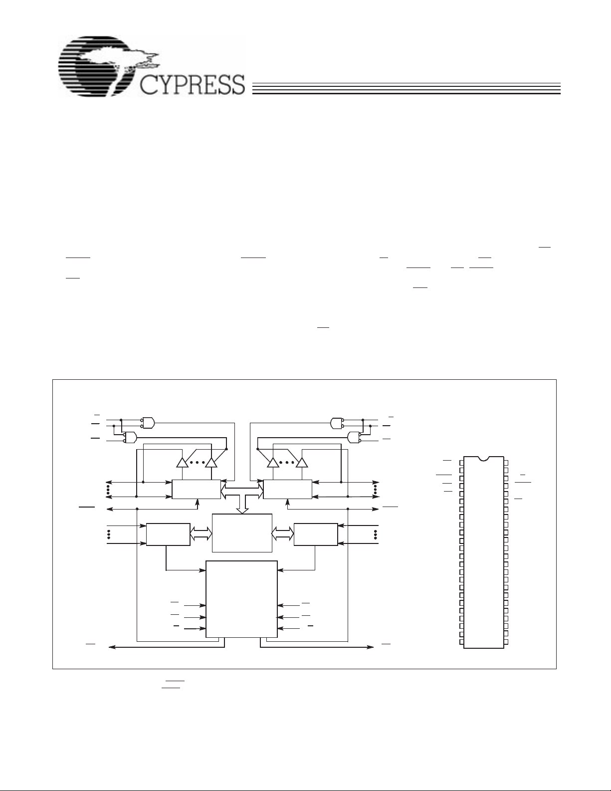
Logic Block Dia gram
R/W
L
CE
L
OE
L
I/O
7L
I/O
0L
[1]
BUSY
L
A
INT
9L
A
0L
[2]
L
ADDRESS
DECODER
Notes:
1. CY7C130/CY7C131 (Master): BUSY
CY7C140/CY7C141 (Slave): BUSY is input.
2. Open drain outputs: pull-up resistor required
s
I/O
CE
OE
R/W
CONTROL
L
L
L
MEMORY
ARRAY
ARBITRATION
LOGIC
(7C130/7C131 ONLY)
AND
INTERRUPT LOGIC
CONTROL
is open drain output and requires pull-up resistor
I/O
Functional Description
The CY7C130/CY7C131/CY7C140 and CY7C141 are
high-speed CMOS 1K by 8 dual-port static RAMs. Two ports
are provided permitting independent access to any location in
memory. The CY7C130/ CY7C131 can be utilized as either a
standalone 8-bit dual-port static RAM or as a master dual-port
RAM in conjunction with the CY7C140/CY7C141 slave dual-port device in systems requiring 16-bit or greater word
widths. It is the solution to applications requiring shared or
buffered data, such as cache memory for DSP, bit-slice, or
multipr ocessor designs.
Each port has independent control pins; chip enable (CE
write enable (R/W
provided on each port, BUSY
), and output enable (OE). Two flags are
and INT. BUSY signals that the
port is trying to access the same location currently being accessed by the other port. INT
is an interrupt flag indicating that
data has been placed i n a u nique loca tion (3FF for the left port
and 3FE for the right port). An automatic power-down feature
is controlled independently on each port by the chip enable
(CE
) pin s.
The CY7C130 and CY7C140 are available in 48-pin DIP. The
CY7C131 and CY7C141 are available in 52-pin PLCC and
PQFP.
Pin Con figurations
R/W
R
CE
R
L
L
L
L
L
0L
1L
2L
3L
4L
5L
6L
7L
8L
9L
0L
1L
2L
3L
4L
5L
6L
7L
DIP
Top View
1
2
3
4
5
6
7
8
9
10
11
12 37
7C130
13
7C140
14
15
16
17
18
19
20
21
22
23 26
24 25
V
48
CC
47
CE
R
R/W
46
BUSY
45
INT
44
OE
43
R
42
A
0R
A
41
1R
40
A
2R
A
39
3R
A
38
4R
A
5R
A
36
6R
A
35
7R
A
34
8R
A
33
9R
I/O
32
7R
31
I/O
6R
I/O
30
5R
I/O
29
4R
I/O
28
3R
I/O
27
2R
I/O
1R
I/O
0R
C130-2
ADDRESS
DECODER
CE
R
OE
R
R/W
R
OE
I/O
I/O
BUSY
A
9R
A
0R
INT
R
7R
0R
R
[2]
R
C130-1
CE
R/W
BUSY
INT
OE
I/O
I/O
I/O
I/O
I/O
I/O
I/O
I/O
GND
A
A
A
A
A
A
A
A
A
A
),
R
R
R
Cypress Semiconductor Corporation • 3901North First Street • San Jose • CA 95134 • 408-943- 2600
May 1989 – Revised March 27, 1997
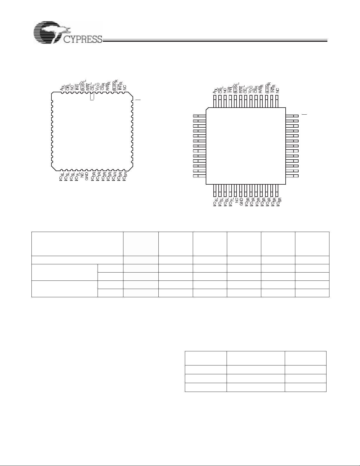
Pin Configuration (continued)
CY7C130/CY7C131
CY7C140/CY7C141
PLCC
Top View
A
A
A
A
A
A
A
A
A
I/O
I/O
I/O
I/O
7 6 5 4 3 2 52 51 50 49 48 47
1L
8
2L
9
3L
10
4L
11
5L
12
6L
13
7L
14
8L
15
9L
16
0L
17
1L
18
2L
19
3L
20
21222324252627282930313233
1
7C131
7C141
OE
46
R
A
45
0R
A
44
1R
A
43
2R
A
42
3R
A
41
4R
A
40
5R
A
39
6R
A
38
7R
A
37
8R
A
36
9R
NC
35
I/O
34
7R
C130-3
A
1L
A
2L
A
3L
A
4L
A
5L
A
6L
A
7L
A
8L
A
9L
I/O
0L
I/O
1L
I/O
2L
I/O
3L
525150 494847 454443424140
1
2
3
4
5
6
7
8
9
10
11
12
13
1415 16 17 18 19 20 21 22 23 24 25 26
PQFP
T op View
46
7C131
7C141
C130-4
OE
A
A
A
A
A
A
A
A
A
A
NC
I/O
R
0R
1R
2R
3R
4R
5R
6R
7R
8R
9R
7R
39
38
37
36
35
34
33
32
31
30
29
28
27
Selectio n Gu ide
7C130-30
7C131-15
7C141-15
[3,4]
7C131-25
7C141-25
[3]
7C131-30
7C140-30
7C141-30
Maximum Access Time (ns) 15 25 30 35 45 55
Maximum Operating
Current (mA)
Maximum Standby
Current (mA)
Com’l/Ind 190 170 170 120 90 90
Milit ary 170 120 120
Com’l/Ind 75 65 65 45 35 35
Milit ary 65 45 45
7C130-35
7C131-35
7C140-35
7C141-35
7C130-45
7C131-45
7C140-45
7C141-45
7C130-55
7C131-55
7C140-55
7C141-55
Maximum Ratings
(Above which the useful life may be impaired. For user guidelines, not tested.)
Storage Temperature ................................. –65°C to +150
Ambient Temperature with
Power Applied.............................................– 55°C to +125°C
Supply Voltage to Ground Potential
(Pin 48 to Pin 24) . ..........................................–0.5V to +7.0V
DC Voltage Applied to Outputs
in High Z State ............................................... –0.5V to +7.0V
DC Input Voltage............................................–3.5V to +7.0V
Output Current into Outputs (LOW).............................20 mA
Notes:
3. 15 and 25-ns version available only in PLCC/PQFP packages.
4. Shaded area contains preliminary information.
5. T
is the “instant on” case temperature
A
°C
Static Discharge Voltage.......................................... >2001V
(per MIL-STD-883, Method 3015)
Latch-Up Current.................................................... >200 mA
Operating Range
Ambient
Range
Commercial 0°C to +70°C 5V ± 10%
Industrial –40°C to +85°C 5V ± 10%
[5]
Military
2
Temperature
V
CC
–55°C to +125°C 5V ± 10%
CY7C130/CY7C131
CY7C140/CY7C141
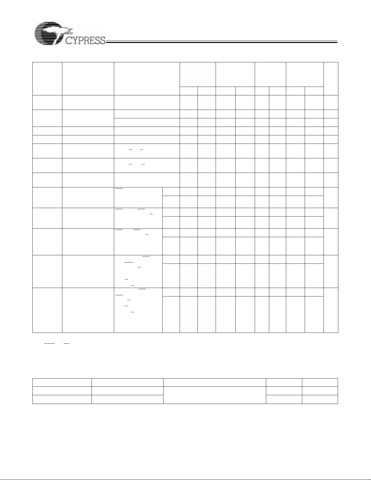
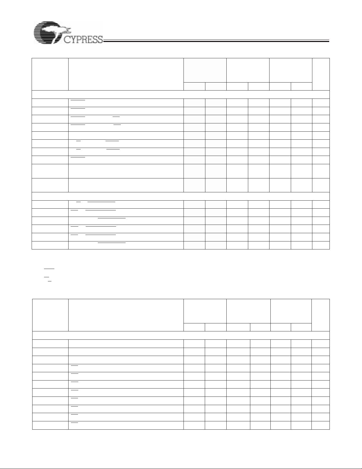
Electrical Characteristics Over the Operating Range
[6]
7C131-15
7C141-15
[3,4]
7C130-30
[3]
7C131-25,30
7C140-30
7C141-25,30
7C130-35
7C131-35
7C140-35
7C141-35
7C130-45,55
7C131-45,55
7C140-45,55
7C141-45,55
Parameter Description Test Conditions Min. Max. Min. Max. Min. Max. Min. Max. Unit
V
OH
V
OL
V
IH
V
IL
I
IX
I
OZ
I
OS
I
CC
I
SB1
I
SB2
I
SB3
I
SB4
Notes:
6. See the last page of this specification for Group A subgroup testing information.
7. BUSY
8. Duration of the short circuit should not exceed 30 seconds.
9. This parameter is guaranteed but not tested.
10. At f=f
Capacitance
Output HIGH
VCC = Min., IOH = –4.0 mA 2.4 2.4 2.4 2.4 V
Voltage
Output LOW
Voltage
IOL = 4.0 mA 0.4 0.4 0.4 0.4 V
IOL = 16.0 mA
[7]
0.5 0.5 0.5 0.5
Input HIGH Voltage 2.2 2.2 2.2 2.2 V
Input LOW Voltage 0.8 0.8 0.8 0.8 V
Input Leakage
Current
Output Leakage
Current
Output Short
Circuit Current
VCC Operating
Supply Current
Standby Current
Both Ports,
TTL Inputs
Standby Current
One Port,
TTL Inputs
Standby Current
Both Ports,
CMOS Inputs
Standby Current
One Port,
CMOS Inputs
and INT pins only.
, address and data inp uts are cycli ng at the maximum fr equency of r ead cycle of 1/tRC and using AC Te st W avefor ms i nput leve ls of GND to 3V.
MAX
[9]
GND < VI < V
GND < VO < VCC,
Output Disabled
VCC = Max.,
[8, 9]
V
OUT
CE = VIL,
Outputs Open,
f = f
CEL and CER >
V
IH
CEL or CER > VIH,
Active Port Outputs Open,
f = f
Both Ports CEL
and CE
0.2V,
V
IN
or V
One Port CEL or
CE
V
IN
or V
Active Port Outputs
Open,
f = f
CC
= GND
[10]
MAX
MAX
[10]
> VCC –
R
[10]
, f = f
MAX
> VCC – 0.2V
< 0.2V, f = 0
IN
> VCC – 0.2V,
R
> VCC – 0.2V
< 0.2 V,
IN
[10]
MAX
–5 +5 –5 +5 –5 +5 –5 +5 µA
–5 +5 –5 +5 –5 +5 –5 +5 µA
–350 –350 –350 –350 mA
Com’l 190 170 120 90 mA
Mil 170 120
Com’l 75 65 45 35 mA
Mil 65 45
Com’l 135 115 90 75 mA
Mil 115 90
Com’l 15 15 15 15 mA
Mil 15 15
Com’l 125 105 85 70 mA
Mil 105 85
Parameter Description Test Conditions Max. Unit
C
IN
C
OUT
]
Input Capacitance TA = 25°C, f = 1 MHz,
V
= 5.0V
Output Capacitance 10 pF
CC
15 pF
3
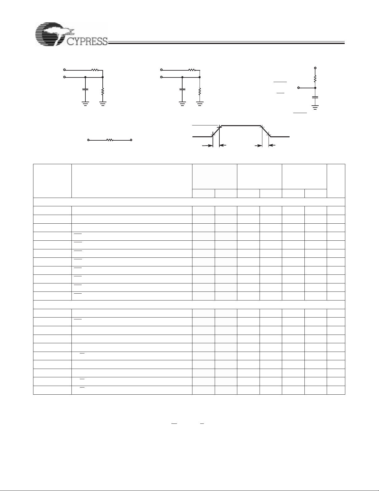
AC Test Loads and Waveforms
V
5V
OUTPUT
INCLUDING
JIGAND
Equivalent to:
R1 893Ω
30 pF
SCOPE
OUTPUT 1.40V
R2
347Ω
(a)
THÉVENIN EQUIVALENT
250Ω
5V
OUTPUT
INCLUDING
5pF
JIGAND
SCOPE
R1 893Ω
(b)
3.0V
GND
≤ 5ns
R2
347Ω
10%
C130-5
ALL INPUT PULSES
90%
CY7C130/CY7C131
CY7C140/CY7C141
5
BUSY
OR
INT
BUSY Output Load
(CY7C130/CY7C131 ONLY)
90%
10%
≤5
ns
281Ω
30
pF
C130-6
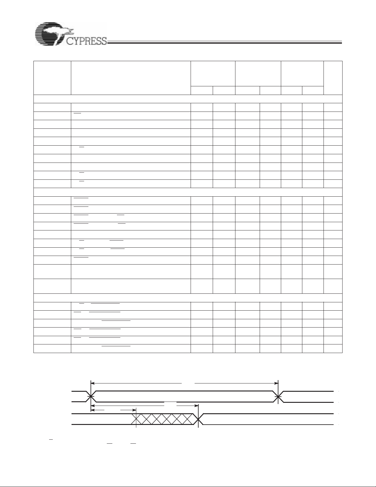
Switching Characteristics Over the Operating Range
Parameter Description
[6,11]
7C131-15
7C141-15
[3,4]
7C130-25
7C131-25
7C140-25
7C141-25
[3]
7C130-30
7C131-30
7C140-30
7C141-30
Min. Max. Min. Max. Min. Max. Unit
READ CYCLE
t
RC
t
AA
t
OHA
t
ACE
t
DOE
t
LZOE
t
HZOE
t
LZCE
t
HZCE
t
PU
t
PD
WRITE CYCLE
t
WC
t
SCE
t
AW
t
HA
t
SA
t
PWE
t
SD
t
HD
t
HZWE
t
LZWE
Notes:
11. Test conditions assume signal transition times of 5 ns or less, timing reference levels of 1.5V, input pulse levels of 0 to 3.0V and output loading of the specified
I
OL/IOH,
12. AC Test Conditions use VOH = 1.6V and VOL = 1.4V.
13. At any given temperature and voltage condition for any given device, t
14. t
LZCE
15. The internal write time of the memory is defined by the overlap of CS LO W and R/W LOW . Both s ignals must be low to ini tiate a write and ei ther s ignal c an terminate
a write by going h igh. T he dat a input set-up and ho ld ti ming shoul d be r efer enced to the ri sing edge of the s ignal that ter minates the write
Read Cycle Time 15 25 30 ns
Address to Data Valid
Data Hold from Address Change 0 00ns
CE LOW to Data Valid
OE LOW to Data Valid
OE LOW to Low Z
OE HIGH to High Z
CE LOW to Low Z
CE HIGH to High Z
CE LOW to Power-Up
CE HIGH to Power-Down
[15]
Write Cycle Time 15 25 30 ns
CE LOW to Write End 12 20 25 ns
Address Set-Up to Write End 12 20 25 ns
Address Hold from Write End 2 22ns
Address Set-Up to Write Start 0 00ns
R/W Pulse Width 12 15 25 ns
Data Set-Up to Write End 10 15 15 ns
Data Hold from Write End 0 00ns
R/W LOW to High Z
R/W HIGH to Lo w Z
and 30-pF load c apacitance.
, t
, t
, t
LZWE
HZOE
LZOE
, t
HZCE
and t
[12]
[12]
[12]
[9,13, 14]
[9,13, 14]
[9,13, 14]
[9,13, 14]
[9]
[9]
[14]
[14]
are tested with CL = 5pF as in par t (b) of AC Test Loads. Transition is measured ±500 m V fro m steady s tate voltage.
HZWE
HZCE
3 33ns
3 55ns
0 00ns
0 00ns
is less than t
15 25 30 ns
15 25 30 ns
10 15 20 ns
10 15 15 ns
10 15 15 ns
15 25 25 ns
10 15 15 ns
and t
LZCE
HZOE
is less than t
LZOE
.
4
CY7C130/CY7C131
CY7C140/CY7C141
Switching Characteristics Over the Operating Range
Parameter Description
[6,11]
(continued)
7C131-15
7C141-15
[3,4]
7C130-25
7C131-25
7C140-25
7C141-25
[3]
7C130-30
7C131-30
7C140-30
7C141-30
Min. Max. Min. Max. Min. Max. Unit
BUSY/INTERRUPT TIMING
t
BLA
t
BHA
t
BLC
t
BHC
t
PS
[17]
t
WB
t
WH
t
BDD
t
DDD
t
WDD
BUSY LOW from Address Match 15 20 20 ns
BUSY HIGH from Address Mismatch
[16]
15 20 20 ns
BUSY LOW from CE LOW 15 20 20 ns
BUSY HIGH from CE HIGH
[16]
15 20 20 ns
Port Set Up for Priority 5 55ns
R/W LOW after BUSY LOW 0 00ns
R/W HIGH after B USY HIGH 13 20 30 ns
BUSY HIGH to Valid Data 15 25 30 ns
Write Data Valid to Read Data Valid Note
18
Write Pulse to Data Delay Note
18
Note
18
Note
18
Note 18ns
Note 18ns
INTERRUPT TIMING
t
WINS
t
EINS
t
INS
t
OINR
t
EINR
t
INR
Notes:
16. These parameters are measured from the input signal changing, until the output pin goes to a high-impedance state.
17. CY7C140/CY7C141 only.
18. A write operation on Port A, where Port A has priority, leaves the data on Port B’s outputs undisturbed until one access time after one of the following:
BUSY
Port B’s addr ess is to ggled.
CE for Port B is toggl ed.
R/W for Port B is tog gled duri ng val id read.
Switching Characteristics Over the Operating Range
R/W to INTERRUPT Set Ti me 15 25 25 ns
CE to INTERRUPT Set Time 15 25 25 ns
Address to INTERRUPT Set T i me 15 25 25 ns
OE to INTERRUPT Reset Time
CE to INTERRUPT Reset Time
Address to INTERRUPT Rese t T im e
on Port B goes H IGH.
[16]
[16]
[16]
[6,1 1]
7C130-35
7C131-35
7C140-35
7C141-35
15 25 25 ns
15 25 25 ns
15 25 25 ns
7C130-4 5
7C131-4 5
7C140-4 5
7C141-4 5
7C130-55
7C131-55
7C140-55
7C141-55
Parameter Description Min. Max. Min. Max. Min. Max. Unit
READ CYCLE
t
RC
t
AA
t
OHA
t
ACE
t
DOE
t
LZOE
t
HZOE
t
LZCE
t
HZCE
t
PU
t
PD
Read Cycle Time 35 45 55 ns
Address to Data Valid
[12]
35 45 55 ns
Data Hold from Address Change 0 0 0 ns
CE LOW to Data Valid
OE LOW to Data Valid
OE LOW to Low Z
OE HIGH to High Z
CE LOW to Low Z
CE HIGH to High Z
CE LOW to Power-Up
CE HIGH to Power-Down
[12]
[12]
[9,13, 14]
[9,13, 14]
[9,13, 14]
[9,13, 14]
[9]
35 45 55 ns
20 25 25 ns
333ns
20 20 25 ns
555ns
20 20 25 ns
000ns
[9]
35 35 35 ns
5
CY7C130/CY7C131
CY7C140/CY7C141
Switching Characteristics Over the Operating Range
[6,1 1]
(continued)
7C130-35
7C131-35
7C140-35
7C141-35
7C130-45
7C131-45
7C140-45
7C141-45
7C130-55
7C131-55
7C140-55
7C141-55
Parameter Description Min. Max. Min. Max. Min. Max. Unit
WRITE CYCLE
t
WC
t
SCE
t
AW
t
HA
t
SA
t
PWE
t
SD
t
HD
t
HZWE
t
LZWE
[15]
Write Cycle Time 35 45 5 5 ns
CE LOW to Write End 30 35 4 0 n s
Address Set-Up to Write End 30 35 40 n s
Address Hold from Write End 2 2 2 ns
Address Set-Up to Write Start 0 0 0 n s
R/W Puls e Wi dth 25 30 30 ns
Data Set-Up to Write End 15 20 2 0 n s
Data Hold from Write End 0 0 0 ns
R/W LOW to High Z
R/W HIGH to Low Z
[14]
[14]
20 20 25 ns
000ns
BUSY/INTERRUPT TIMING
t
BLA
t
BHA
t
BLC
t
BHC
t
PS
t
WB
t
WH
t
BDD
t
DDD
t
WDD
[17]
BUSY LOW from Address Match 20 25 30 ns
BUSY HIGH from Address Mismatch
[16]
20 25 30 ns
BUSY LOW from CE LOW 20 25 30 ns
BUSY HIGH from CE HIGH
[16]
20 25 30 ns
Port Set Up for Priority 5 5 5 ns
R/W LOW after BUSY LOW 0 0 0 ns
R/W HIGH after BUSY HI GH 30 35 35 ns
BUSY HIGH to Valid Data 35 45 45 ns
Write Data Valid to Read Data Valid Note
18
Write Pulse to Data Delay Note
18
Note
18
Note
18
Note 18ns
Note 18ns
INTERRUPT TIMING
t
WINS
t
EINS
t
INS
t
OINR
t
EINR
t
INR
R/W to INTERRUP T S et Tim e 25 35 45 ns
CE to INTERRUPT Set Time 25 35 45 n s
Address to INTERRUPT Se t Tim e 25 35 45 ns
OE to INTERRUPT Reset Time
CE to INTERRUPT Reset Time
Address to INTERRUPT Reset Time
[16]
[16]
[16]
25 35 45 ns
25 35 45 ns
25 35 45 ns
Switching Waveforms
Read Cycle No.1
ADDRESS
DATA OUT
Notes:
is HIGH for rea d c ycle.
19. R/W
20. Device is continuously selected, CE = VIL and OE = VIL.
[19, 20]
t
OHA
Either Port Address Access
t
RC
t
AA
6
DATA VALIDPREVIOUS DATA VALID
C130-7

Switching Waveforms (continued)
Read Cycle No. 2
CE
OE
DATA OUT
I
CC
I
SB
Read Cycle No.3
ADDRESS
R/W
D
R
R
INR
[19, 21]
[20]
t
LZOE
t
LZCE
t
PU
Read with BUSY, Master: CY7C130 and CY7C131
t
ACE
Either Port CE/OE Access
t
DOE
t
RC
ADDRESS MATCH
t
PWE
DATA VALID
VALID
CY7C130/CY7C131
CY7C140/CY7C141
t
HZCE
t
HZOE
t
PD
t
HD
C130-8
ADDRESS
Write CycleNo.1 (OE Three-States Data I/Os - Either Port)
BUSY
DOUT
L
t
PS
L
t
BLA
L
[15, 22]
Either Port
t
WC
ADDRESS
t
SCE
CE
t
t
SA
AW
R/W
DATA
IN
OE
t
HZOE
HIGH IMPEDANCE
D
OUT
Notes:
21. Address valid prior to or coincident with CE
22. If OE is LOW during a R/W controlled write cycl e, the write pulse width must be the larger of t
to be placed on the bus for the req uired tSD.
transition LOW.
ADDRESS MATCH
t
WDD
t
PWE
t
SD
DATA VALID
or t
PWE
+ tSD to allow the data I/O pins to enter high impedance and f or data
HZWE
t
DDD
t
t
BHA
HD
t
BDD
VALID
C130-9
t
HA
C130-10
7

Switching Waveforms (continued)
Write Cycle No. 2 (R/W Three-States Data I/Os - Either Port)
Either Port
t
WC
ADDRESS
t
SCE
CE
t
AW
R/W
t
SA
[16, 23]
t
PWE
CY7C130/CY7C131
CY7C140/CY7C141
t
HA
DATA
IN
DATA
OUT
Busy Timing Diagram No. 1 (CE Arbitration)
CELValid First:
ADDRESS
CE
CE
BUSY
L,R
L
t
PS
R
R
CERValid First:
t
HZWE
ADDRESS MATCH
t
BLC
t
SD
t
HD
DATAVALID
t
LZWE
HIGH IMPEDANCE
t
BHC
C130-11
C130-12
ADDRESS
BUSY
Note:
23. If the CE
L,R
CE
R
CE
L
L
LOW transition occurs simul taneously with or after th e R/W L OW transi tion, the ou tputs r emain in the hi gh-impedan ce state
ADDRESS MATCH
t
PS
t
BLC
t
BHC
8
C130-13

Switching Waveforms (continued)
Busy Timing Diagram No. 2 (Address Arbitration)
Left Address Valid First:
t
or t
RC
WC
ADDRESS
L
ADDRESS MATCH
t
PS
CY7C130/CY7C131
CY7C140/CY7C141
ADDRESS MISMATCH
ADDRESS
BUSY
R
R
t
BLA
Right Address Valid First:
tRCor t
WC
ADDRESS MATCH ADDRESS MISMATCH
ADDRESS
ADDRESS
BUSY
R
L
L
t
PS
t
BLA
Busy Timing Diagram No. 3
Write with BUSY (Slave:CY7C140/CY7C141)
CE
t
BHA
t
BHA
C130-14
C130-15
R/W
BUSY
t
WB
t
PWE
9
t
WH
C130-16

Switching Waveforms (continued)
Interrupt Timing Diagrams
CY7C130/CY7C131
CY7C140/CY7C141
Left Side Sets INT
ADDR
L
CE
L
R/W
L
INT
R
R
Right Side Clears INT
ADDR
R
CE
R
R/W
R
OE
R
INT
R
t
WC
WRITE 3FF
t
INS
t
EINS
t
SA
R
t
WINS
t
HA
C130-17
t
RC
READ 3FF
t
EINR
t
HA
t
INT
t
OINR
C130-18
Right Side Sets INT
ADDR
R
CE
R
R/W
R
INT
L
Left Side Clears INT
ADDR
R
CE
L
R/W
L
OE
L
INT
L
L
t
WC
WRITE 3FE
WINS
t
HA
C130-19
t
RC
t
INS
t
EINS
t
SA
L
t
READ 3FE
t
EINR
t
HA
t
INR
t
OINR
C130-20
10

T y pical DC and AC Characteristics
CY7C130/CY7C131
CY7C140/CY7C141
NORMALIZED SUPPLY CURRENT
vs.SUPPLYVOLTAGE
1.4
1.2
I
CC
1.0
0.8
0.6
0.4
0.2
0.0
4.0 4.5 5.0 5.5 6.0
I
SB3
SUPPLY VOLTAGE ( V)
NORMALIZED ACCES S TIME
vs. SUPPLY VOLTAGE
1.4
1.3
1.2
1.1
T
=25°C
1.0
A
0.9
0.8
4.0 4.5 5.0 5.5 6.0
SUPPLYVOLTAGE (V)
NORMALIZED SUPP LY CURRENT
vs. AMBIENT TEMPERATURE
1.2
I
1.0
CC
0.8
0.6
0.4
0.2
0.6
-55 25 125
VCC=5.0V
V
=5.0V
IN
I
SB3
AMBIENT TEMPERATURE (°C)
NORMALIZED ACCES S TIME
vs. AMBIENT TEMPERATURE
1.6
1.4
1.2
1.0
=5.0V
V
CC
0.8
0.6
-55 125
25
AMBIENT TEMPERATURE (°C)
OUTPUT SOURCE CURRENT
vs. OUTPUT VOLTAGE
120
100
80
60
40
V
CC
T
A
=5.0V
=25°C
20
0
0 1.0 2.0 3.0 4.0
OUTPUT VOLTAGE(V)
OUTPUT SINK CURRENT
vs.OUTPUT VOLTAGE
140
120
100
80
60
40
V
=5.0V
20
T
CC
=25°C
A
0
0.0 1.0 2.0 3.0 4.0
OUTPUT VOLTAGE(V)
TYPICAL POWER -ON CURRENT
vs. SUPPLY VOLTAGE
3.0
2.5
2.0
1.5
1.0
0.5
0.0
0 1.0 2 .0 3.0 5.0
4.0
SUPPLYVOLTAGE(V)
TYPICAL ACCESS TIME CHANGE
vs. OUTPUT LOADING
30.0
25.0
20.0
15.0
10.0
=4.5V
V
5.0
0
0 200 400 600 800
T
CC
=25°C
A
CAPACITANCE (pF)
11
1000
NORMALIZED I
1.25
V
T
A
V
CC
=25°C
=0.5V
IN
=4.5V
vs.CYCLETIME
CC
1.0
0.75
0.50
10 40
20 30
CYCLE FREQUENCY (MHz)

Ordering Info rma tio n
CY7C130/CY7C131
CY7C140/CY7C141
Speed
(ns) Ordering Code
30 CY7C130-30PC P25 48-Lead (600-Mil) Molded DIP Commercial
CY7C130-30PI P25 48-Lead (600-Mil) Molded DIP Industrial
35 CY7C130-35PC P25 48-Lead (600-Mil) Molded DIP Commercial
CY7C130-35PI P25 48-Lead (600-Mil) Molded DIP Industrial
CY7C130-35DMB D26 48-Lead (600-Mil) Sidebraze DIP Military
45 CY7C130-45PC P25 48-Lead (600-Mil) Molded DIP Commercial
CY7C130-45PI P25 48-Lead (600-Mil) Molded DIP Industrial
CY7C130-45DMB D26 48-Lead (600-Mil) Sidebraze DIP Military
55 CY7C130-55PC P25 48-Lead (600-Mil) Molded DIP Commercial
CY7C130-55PI P25 48-Lead (600-Mil) Molded DIP Industrial
CY7C130-55DMB D26 48-Lead (600-Mil) Sidebraze DIP Military
Speed
(ns) Orderi ng Code
15 CY7C131-15JC J69 52-Lead Plastic Leaded Chip Carrier Commercial
CY7C131-15NC N52 52-Pin Plastic Quad Flatpack
25 CY7C131-25JC J69 52-Lead Plastic Leaded Chip Carrier Commercial
CY7C131-25NC N52 52-Pin Plastic Quad Flatpack
CY7C131-25JI J69 52-Lead Plastic Leaded Chip Carrier Industrial
CY7C131-25NI N52 52-Pin Plastic Quad Flatpack
30 CY7C131-30JC J69 52-Lead Plastic Leaded Chip Carrier Commercial
CY7C131-30NC N52 52-Pin Plastic Quad Flatpack
CY7C131-30JI J69 52-Lead Plastic Leaded Chip Carrier Industrial
35 CY7C131-35JC J69 52-Lead Plastic Leaded Chip Carrier Commercial
CY7C131-35NC N52 52-Pin Plastic Quad Flatpack
CY7C131-35JI J69 52-Lead Plastic Leaded Chip Carrier Industrial
CY7C131-35NI N52 52-Pin Plastic Quad Flatpack
45 CY7C131-45JC J69 52-Lead Plastic Leaded Chip Carrier Commercial
CY7C131-45NC N52 52-Pin Plastic Quad Flatpack
CY7C131-45JI J69 52-Lead Plastic Leaded Chip Carrier Industrial
CY7C131-45NI N52 52-Pin Plastic Quad Flatpack
55 CY7C131-55JC J69 52-Lead Plastic Leaded Chip Carrier Commercial
CY7C131-55NC N52 52-Pin Plastic Quad Flatpack
CY7C131-55JI J69 52-Lead Plastic Leaded Chip Carrier Industrial
CY7C131-55NI N52 52-Pin Plastic Quad Flatpack
Shaded area contains preliminary information.
Package
Name Package Type
Package
Name Package Type
Operating
Operating
Range
Range
12

Ordering Info rma tio n (continued)
CY7C130/CY7C131
CY7C140/CY7C141
Speed
(ns) Ordering Code
30 CY7C140-30PC P25 48-Lead (600-Mil) Molded DIP Commercial
CY7C140-30PI P25 48-Lead (600-Mil) Molded DIP Industrial
35 CY7C140-35PC P25 48-Lead (600-Mil) Molded DIP Commercial
CY7C140-35PI P25 48-Lead (600-Mil) Molded DIP Industrial
CY7C140-35DMB D26 48-Lead (600-Mil) Sidebraze DIP Military
45 CY7C140-45PC P25 48-Lead (600-Mil) Molded DIP Commercial
CY7C140-45PI P25 48-Lead (600-Mil) Molded DIP Industrial
CY7C140-45DMB D26 48-Lead (600-Mil) Sidebraze DIP Military
55 CY7C140-55PC P25 48-Lead (600-Mil) Molded DIP Commercial
CY7C140-55PI P25 48-Lead (600-Mil) Molded DIP Industrial
CY7C140-55DMB D26 48-Lead (600-Mil) Sidebraze DIP Military
Speed
(ns) Orderi ng Code
15 CY7C141-15JC J69 52-Lead Plastic Leaded Chip Carrier Commercial
CY7C141-15NC N52 52-Pin Plastic Quad Flatpack
25 CY7C141-25JC J69 52-Lead Plastic Leaded Chip Carrier Commercial
CY7C141-25NC N52 52-Pin Plastic Quad Flatpack
CY7C141-25JI J69 52-Lead Plastic Leaded Chip Carrier Industrial
CY7C141-25NI N52 52-Pin Plastic Quad Flatpack
30 CY7C141-30JC J69 52-Lead Plastic Leaded Chip Carrier Commercial
CY7C141-30NC N52 52-Pin Plastic Quad Flatpack
CY7C141-30JI J69 52-Lead Plastic Leaded Chip Carrier Industrial
35 CY7C141-35JC J69 52-Lead Plastic Leaded Chip Carrier Commercial
CY7C141-35NC N52 52-Pin Plastic Quad Flatpack
CY7C141-35JI J69 52-Lead Plastic Leaded Chip Carrier Industrial
CY7C141-35NI N52 52-Pin Plastic Quad Flatpack
45 CY7C141-45JC J69 52-Lead Plastic Leaded Chip Carrier Commercial
CY7C141-45NC N52 52-Pin Plastic Quad Flatpack
CY7C141-45JI J69 52-Lead Plastic Leaded Chip Carrier Industrial
CY7C141-45NI N52 52-Pin Plastic Quad Flatpack
55 CY7C141-55JC J69 52-Lead Plastic Leaded Chip Carrier Commercial
CY7C141-55NC N52 52-Pin Plastic Quad Flatpack
CY7C141-55JI J69 52-Lead Plastic Leaded Chip Carrier Industrial
CY7C141-55NI N52 52-Pin Plastic Quad Flatpack
Shaded area contains preliminary information.
Package
Name Package Type
Package
Name Package Type
Operating
Operating
Range
Range
13

CY7C130/CY7C131
CY7C140/CY7C141
MILITARY SPECIFICATIONS
Group A Subgroup Testing
DC Characteristics
Parameter Subgroups
V
OH
V
OL
V
IH
VIL Max. 1, 2, 3
I
IX
I
OZ
I
CC
I
SB1
I
SB2
I
SB3
I
SB4
1, 2, 3
1, 2, 3
1, 2, 3
1, 2, 3
1, 2, 3
1, 2, 3
1, 2, 3
1, 2, 3
1, 2, 3
1, 2, 3
Switching Characteristics
Parameter Subgroups
READ CYCLE
t
RC
t
AA
t
ACE
t
DOE
WRITE CYCLE
t
WC
t
SCE
t
AW
t
HA
t
SA
t
PWE
t
SD
t
HD
Parameter Subgroups
BUSY/INTERRUPT TIMING
t
BLA
t
BHA
t
BLC
t
BHC
t
PS
t
WINS
t
EINS
t
INS
t
OINR
t
EINR
t
INR
BUSY TIMING
[24]
t
WB
t
WH
t
BDD
Note:
24. CY7C140/CY7C141 only.
Document #: 38-00027-L
r
7, 8, 9, 10, 11
7, 8, 9, 10, 11
7, 8, 9, 10, 11
7, 8, 9, 10, 11
7, 8, 9, 10, 11
7, 8, 9, 10, 11
7, 8, 9, 10, 11
7, 8, 9, 10, 11
7, 8, 9, 10, 11
7, 8, 9, 10, 11
7, 8, 9, 10, 11
7, 8, 9, 10, 11
7, 8, 9, 10, 11
7, 8, 9, 10, 11
7, 8, 9, 10, 11
7, 8, 9, 10, 11
7, 8, 9, 10, 11
7, 8, 9, 10, 11
7, 8, 9, 10, 11
7, 8, 9, 10, 11
7, 8, 9, 10, 11
7, 8, 9, 10, 11
7, 8, 9, 10, 11
7, 8, 9, 10, 11
7, 8, 9, 10, 11
7, 8, 9, 10, 11
14

Package Diagrams
CY7C130/CY7C131
CY7C140/CY7C141
48-Lead (600-Mil) Sidebraze DIP D26
52-Lead Plastic LeadedChip Carrier
J69
15

Package Diagrams (continued)
CY7C130/CY7C131
CY7C140/CY7C141
48-Lead (600-Mil) Molded DIP
P25
© Cypress Semiconductor Corporation, 1997. The information contained herein is subject to change without notice. Cypress Semiconductor Corporation assumes no responsibility for the use
of any circuitry other than c ircui try embodied in a Cyp ress Semiconduc tor product. Nor does it con vey or impl y any license under p atent o r other ri ghts. Cypres s Semi conductor does not authoriz e
its products for use as critical components in life-support systems where a malfunction or failure may reasonably be expected to result in significant injury to the user. The inclusion of Cypress
Semiconductor products in life-support systems application implies that the manufacturer assumes all risk of such use and in doing so indemnifies Cypress Semiconductor against all charges.

WWW.ALLDATASHEET.COM
Copyright © Each Manufacturing Company.
All Datasheets cannot be modified without permission.
This datasheet has been download from :
www.AllDataSheet.com
100% Free DataSheet Search Site.
Free Download.
No Register.
Fast Search System.
www.AllDataSheet.com
 Loading...