

Page 1
CY7C1297H
A
A
B
1-Mbit (64K x 18) Flow-Through Sync SRAM
Features
• 64K x 18 common I/O
• 3.3V core power supply (V
• 2.5V/3.3V I/O power supply (V
DD
)
DDQ
)
• Fast clock-to-output times
— 6.5 ns (for 133-MHz version )
• Provide high-performance 2-1-1-1 access rate
• User-selectable burst counter supporting Intel
Pentium
®
interleaved or linear burst sequences
®
• Separate processor and controller address strobes
• Synchronous self-timed write
• Asynchronous output enable
• Available in JEDEC-standard lead-free 100-Pin TQFP
package
• “ZZ” Sleep Mode option
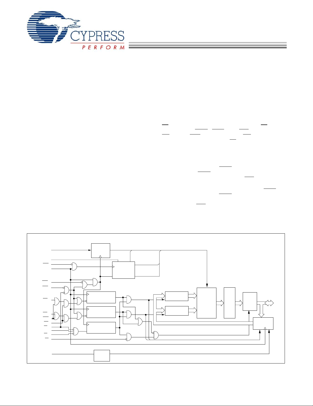
Logic Block Diagram
Functional Description
[1]
The CY7C1297H is a 64K x 18 synchronous cache RAM
designed to interface with high-speed microprocessors with
minimum glue logic. Maximum access delay from clock rise is
6.5 ns (133-MHz version). A 2-bit on-chip counter captures the
first address in a burst and increments the address automatically for the rest of the burst access. All synchronous inputs
are gated by registers controlled by a positive-edge-trigg ered
Clock Input (CLK). The synchronous inputs include all
addresses, all data inputs, address-pipelining Chip Enable
(
)
, depth-expansion Chip Enables (CE
CE
1
Control inputs (ADSC, ADSP
(BW
inputs include the Output Enable (OE
, and BWE), and Global Write (GW). Asynchronous
[A:B]
,
and
and
2
ADV), Write Enables
CE
), Burst
3
) and the ZZ pin.
The CY7C1297H allows either interleaved or linear burst
sequences, selected by the MODE input pin. A HIGH selects
an interleaved burst sequence, while a LOW selects a linear
burst sequence. Burst accesses can be initiated with the
Processor Address Strobe (ADSP
Address Strobe (ADSC
) inputs. Address advancement is
controlled by the Address Advancement (ADV
) or the cache Controller
) input.
Addresses and chip enables are registered at rising edge of
clock when either Address Strobe Processor (ADSP
Address Strobe Controller (ADSC
) are active. Subsequent
) or
burst addresses can be internally generated as controlled by
the Advance pin (ADV).
The CY7C1297H operates from a +3.3V core power supply
while all outputs may operate either with a +2.5V or +3.3 V
supply. All inputs and outputs are JEDEC-standard
JESD8-5-compatible.
0,A1,A
MODE
ADV
CLK
ADSC
ADSP
BW
B
BW
A
BWE
GW
CE
1
CE
2
CE
3
OE
ZZ
Note:
1. For best-practices recommendations, please refer to the Cypress application note System Design Guidelines on www.cypress.com.
ADDRESS
REGISTER
DQB,DQP
DQ
A
,DQP
ENABLE
REGISTER
SLEEP
CONTROL
B
A
WRITE REGISTER
WRITE REGISTER
BURST
COUNTER AND
LOGIC
CLR
Q1
Q0
A[1:0]
DQB,DQP
B
WRITE DRIVER
DQ
A
,DQP
A
WRITE DRIVER
MEMORY
ARRAY
SENSE
AMPS
OUTPUT
BUFFERS
INPUT
REGISTERS
DQs
DQP
DQP
Cypress Semiconductor Corporation • 198 Champion Court • San Jose, CA 95134-1709 • 408-943-2600
Document #: 38-05669 Rev. *B Revised July 6, 2006
[+] Feedback
Page 2
CY7C1297H
Selection Guide
133 MHz 100 MHz Unit
Maximum Access Time 6.5 8.0 ns
Maximum Operating Current 225 205 mA
Maximum Standby Current
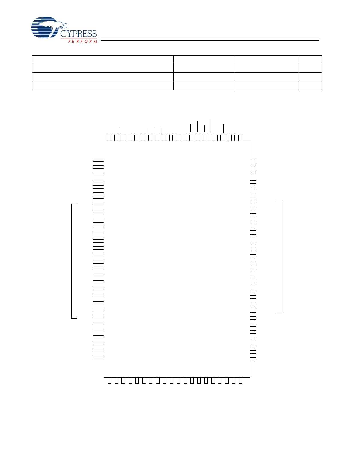
Pin Configuration
100-Pin TQFP
40 40 mA
BYTE B
V
DDQ
V
DQ
DQ
V
V
DDQ
DQ
DQ
V
NC
V
DQ
DQ
V
DDQ
V
DQ
DQ
DQP
V
V
DDQ
NC
NC
NC
SS
NC
NC
SS
NC
DD
SS
SS
NC
SS
NC
NC
NC
A
100
CE
CE
NC
NC
99989796959493929190898887868584838281
2
1
A
1
2
3
4
5
6
7
8
B
9
B
10
11
12
B
13
B
14
15
16
17
18
B
19
B
20
21
22
B
23
B
24
B
25
26
27
28
29
30
3
BBWA
CE
BW
VDDV
CY7C1297H
SS
GW
CLK
ADSP
ADV
A
A
80
79
78
77
76
75
74
73
72
71
70
69
68
67
66
65
64
63
62
61
60
59
58
57
56
55
54
53
52
51
A
NC
NC
V
DDQ
V
SS
NC
DQP
DQ
DQ
V
SS
V
DDQ
DQ
DQ
V
SS
NC
V
DD
ZZ
DQ
DQ
V
DDQ
V
SS
DQ
DQ
NC
NC
V
SS
V
DDQ
NC
NC
NC
A
A
A
A
A
BYTE A
A
A
A
A
ADSC
BWE
OE
31323334353637383940414243444546474849
AAAAA1A
MODE
0
NC/72M
NC/36M
SS
DD
V
V
NC/9M
NC/18M
AAAAA
NC/2M
50
NC/4M
Document #: 38-05669 Rev. *B Page 2 of 15
[+] Feedback
Page 3
CY7C1297H
Pin Descriptions
Name I/O Description
A0, A1, A Input-
Synchronous
BWA, BW
B
Input-
Synchronous
GW Input-
Synchronous
BWE
Input-
Synchronous
CLK Input-
Clock
CE
CE
CE
1
2
3
Input-
Synchronous
Input-
Synchronous
Input-
Synchronous
OE Input-
Asynchronous
ADV Input-
Synchronous
ADSP
Input-
Synchronous
ADSC
Input-
Synchronous
ZZ Input-
Asynchronous
DQs
DQP
V
DD
V
SS
V
DDQ
A,
DQP
B
I/O-
Synchronous
Power Supply Power supply inputs to the core of the device.
Ground Ground for the device.
I/O Power
Supply
MODE Input-
Static
NC No Connects. Not Internally connected to the die. 2M, 4M, 9M, 18M, 72M, 144M, 288M, 576M
Address Inputs used to select one of the 64K address locations. Sampled at the rising edge
of the CLK if ADSP or ADSC is active LOW, and CE1, CE2, and CE3 are sampled active. A
feed the 2-bit counter.
[1:0]
Byte Write Select Inputs, active LOW. Qualified with BWE to conduct Byte W rites to the SRAM.
Sampled on the rising edge of CLK.
Global Write Enable Input, active LOW. When asserted LOW on the rising edge of CLK, a global
Write is conducted (ALL bytes are written, regardless of the values on BW
and BWE).
[A:B]
Byte Write Enable Input, active LOW. Sampled on the rising edge of CLK. This signal must be
asserted LOW to conduct a Byte Write.
Clock Input. Used to capture all synchronous inputs to the device. Also used to increment the
burst counter when ADV
is asserted LOW, during a burst operation.
Chip Enable 1 Input, active LOW. Sampled on the rising edge of CLK. Used in conjunction with
and CE3 to select/deselect the device. ADSP is ignored if CE1 is HIGH. CE1 is sampled only
CE
2
when a new external address is loaded.
Chip Enable 2 Input, active HIGH. Sampled on the rising edge of CLK. Used in conjunction with
CE
and CE3 to select/deselect the device. CE
1
loaded.
is sampled only when a new external address is
2
Chip Enable 3 Input, active LOW. Sampled on the rising edge of CLK. Used in conjunction with
CE
and CE2 to select/deselect the device. CE3 is sampled only when a new external address is
1
loaded.
Output Enable, asynchronous input, active LOW . Controls the direction of the I/O pins. When
LOW, the I/O pins behave as outputs. When deasserted HIGH, I/O pins are tri-stated, and act as
input data pins. OE is masked during the first clock of a Read cycle when emerging from a
deselected state.
Advance Input signal, sampled on the rising edge of CLK. When asserted, it automatically
increments the address in a burst cycle.
Address Strobe from Processor, sampled on the rising edge of CLK, active LOW. When
asserted LOW, addresses presented to the device are captured in the address registers. A
are also loaded into the burst counter. When ADSP
recognized. ASDP
is ignored when
CE1 is deasserted HIGH
and ADSC are both asserted, only ADSP is
[1:0]
Address Strobe from Controller, sampled on the rising edge of CLK, active LOW. When
asserted LOW, addresses presented to the device are captured in the address registers. A
are also loaded into the burst counter. When ADSP
and ADSC are both asserted, only ADSP is
[1:0]
recognized.
ZZ “Sleep” Input, active HIGH. When asserted HIGH places the device in a non-time-critical
“sleep” condition with data integrity preserved. For normal operation, this pin has to be LOW or
left floating. ZZ pin has an internal pull-down.
Bidirectional Data I/O lines. As inputs, they feed into an on-chip data register that is triggered
by the rising edge of CLK. As outputs, they deliver the data contained in the memory location
specified by the addresses presented during the previous clock rise of the Read cycle. The
direction of the pins is controlled by OE
When HIGH, DQs and DQP
[A:B]
. When OE is asserted LOW, the pins behave as outputs.
are placed in a tri-state condition.
Power supply for the I/O circuitry.
Selects Burst Order. When tied to GND selects linear burst sequence. When tied to V
floating selects interleaved burst sequence. This is a strap pin and should remain static during
DD
or left
device operation. Mode Pin has an internal pull-up.
and 1G are address expansion pins and are not internally connected to the die.
Document #: 38-05669 Rev. *B Page 3 of 15
[+] Feedback
Page 4

CY7C1297H
Functional Overview
All synchronous inputs pass through input registers controlled
by the rising edge of the clock. Maximum access d elay from
the clock rise (t
The CY7C1297H supports secondary cache in systems
utilizing either a linear or interleaved burst sequence. The
interleaved burst order supports Pentium and i486™
processors. The linear burst sequence is suited for processors
that utilize a linear burst sequence. The burst order is
user-selectable, and is determined by sampling the MODE
input. Accesses can be initiated with either the Processor
Address Strobe (ADSP
). Address advancement through the burst sequence is
(ADSC
controlled by the ADV
burst counter captures the first address in a burst sequence
and automatically increments the address for the rest of the
burst access.
Byte Write operations are qualified with the Byte Write Enable
(BWE
) and Byte Write Select (BW
Enable (GW
all four bytes. All writes are simplified with on-chip
synchronous self-timed write circuitry.
Three synchronous Chip Selects (CE
asynchronous Output Enable (OE
selection and output tri-state control. ADSP
is HIGH.
Single Read Accesses
A single read access is initiated when the following conditions
are satisfied at clock rise: (1) CE
asserted active, and (2) ADSP
the access is initiated by ADSC
deasserted during this first cycle). The address presented to
the address inputs is latched into the address register and the
burst counter/control logic and presented to the memory core.
If the OE input is asserted LOW, the requested data will be
available at the data outputs a maximum to t
rise. ADSP
is ignored if CE1 is HIGH.
Single Write Accesses Initiated by ADSP
This access is initiated when the following conditions are
satisfied at clock rise: (1) CE
active, and (2) ADSP
presented are loaded into the address register and the burst
inputs (GW
, BWE, and BW
clock cycle. If the Write inputs are asserted active (see Write
Cycle Descriptions table for appropriate states that indicate a
Write) on the next clock rise, the appropriate data will be
latched and written into the device. Byte Writes are allowed.
During byte writes, BW
All I/Os are tri-stated during a Byte Write. Since this is a
common I/O device, the asynchronous OE input signal must
be deasserted and the I/Os must be tri-stated prior to the
presentation of data to DQs. As a safety precaution, the data
lines are tri-stated once a Write cycle is detected, regardless
of the state of OE
Single Write Accesses Initiated by ADSC
This write access is initiated when the following conditions are
satisfied at clock rise: (1) CE
) is 6.5 ns (133-MHz device).
CDV
) or the Controller Address Strobe
input. A two-bit on-chip wraparound
) inputs. A Global Write
) overrides all byte write inputs and writes data to
[A:D]
, CE2, CE3) and an
1
) provide for easy bank
is ignored if CE
, CE2, and CE3 are all
1
or ADSC is asserted LOW (if
, the write inputs must be
after clock
CDV
, CE2, CE3 are all asserted
1
is asserted LOW. The addresses
) are ignored during this first
[A:B]
controls DQA and BWB controls DQB.
A
.
, CE2, and CE3 are all asserted
1
active, (2) ADSC
HIGH, and (4) the Write input signals (GW
indicate a write access. ADSC
is asserted LOW, (3) ADSP is deasserted
, BWE, and BW
is ignored if ADSP is active
LOW.
The addresses presented are loaded into the address register
and the burst counter/control logic and delivered to the
memory core. The information presented to DQ
written into the specified address location. Byte Writes are
allowed. During Byte Writes, BWA controls DQA and BW
controls DQB. All I/Os are tri-stated when a write is detected,
even a Byte Write. Since this is a common I/O device, the
asynchronous OE input signal must be deasserted and the
I/Os must be tri-stated prior to the presentation of data to DQs.
As a safety precaution, the data lines are tri-stated once a
Write cycle is detected, regardless of the state of OE
Burst Sequences
The CY7C1297H provides an on-chip two-bit wraparound burst
counter inside the SRAM. The burst counter is fed by A
and can follow either a linear or interleaved burst order. The
burst order is determined by the state of the MODE input. A
LOW on MODE will select a linear burst sequence. A HIGH on
MODE will select an interleaved burst order. Leaving MODE
unconnected will cause the device to default to a interleaved
burst sequence.
Sleep Mode
1
The ZZ input pin is an asynchronous input. Asserting ZZ
places the SRAM in a power conservation “sleep” mode. Two
clock cycles are required to enter into or exit from this “sleep”
mode. While in this mode, data integrity is guaranteed.
Accesses pending when entering the “sleep” mode are not
considered valid nor is the completion of the operation
guaranteed. The device must be deselected prior to entering
the “sleep” mode. CE
inactive for the duration of t
LOW.
s, ADSP, and ADSC must remain
after the ZZ input returns
ZZREC
Interleaved Burst Address Table
(MODE = Floating or V
First
Address
A1, A0
00 01 10 11
01 00 11 10
10 11 00 01
11 10 01 00
Second
Address
A1, A0
DD
)
Third
Address
A1, A0
Linear Burst Address Table
(MODE = GND)
First
Address
A1, A
0
00 01 10 11
01 10 11 00
10 11 00 01
11 00 01 10
Second
Address
A1, A
0
Third
Address
A1, A
0
will be
[A:B]
.
[1:0]
Fourth
Address
A1, A0
Fourth
Address
A1, A
0
[A:B]
)
B
,
Document #: 38-05669 Rev. *B Page 4 of 15
[+] Feedback
Page 5
CY7C1297H
ZZ Mode Electrical Characteristics
Parameter Description Test Conditions Min. Max. Unit
I
DDZZ
t
ZZS
t
ZZREC
t
ZZI
t
RZZI
Truth Table
Cycle Description Address Used CE1CE2CE3ZZ ADSP ADSC ADV WRITE OE CLK DQ
Deselected Cycle,
Power-down
Deselected Cycle,
Power-down
Deselected Cycle,
Power-down
Deselected Cycle,
Power-down
Deselected Cycle,
Power-down
Sleep Mode, Power-down None X X X H X X X X X X Tri-State
Read Cycle, Begin Burst External L H L L L X X X L L-H Q
Read Cycle, Begin Burst External L H L L L X X X H L-H Tri-State
Write Cycle, Begin Burst External L H L L H L X L X L-H D
Read Cycle, Begin Burst External L H L L H L X H L L-H Q
Read Cycle, Begin Burst External L H L L H L X H H L-H Tri-State
Read Cycle, Continue Burst Next X X X L H H L H L L-H Q
Read Cycle, Continue Burst Next X X X L H H L H H L-H Tri-State
Read Cycle, Continue Burst Next H X X L X H L H L L-H Q
Read Cycle, Continue Burst Next H X X L X H L H H L-H Tri-State
Write Cycle, Continue Burst Next X X X L H H L L X L-H D
Write Cycle, Continue Burst Next H X X L X H L L X L-H D
Read Cycle, Suspend Burst Current X X X L H H H H L L-H Q
Read Cycle, Suspend Burst Current X X X L H H H H H L-H Tri-State
Read Cycle, Suspend Burst Current H X X L X H H H L L-H Q
Read Cycle, Suspend Burst Current H X X L X H H H H L-H Tri-State
Write Cycle, Suspend Burst Current X X X L H H H L X L-H D
Write Cycle, Suspend Burst Current H X X L X H H L X L-H D
Sleep mode standby current ZZ > VDD – 0.2V 40 mA
Device operation to ZZ ZZ > VDD – 0.2V 2t
ZZ recovery time ZZ < 0.2V 2t
CYC
ZZ Active to sleep current This parameter is sampled 2t
CYC
CYC
ZZ Inactive to exit sleep current This parameter is sampled 0 ns
[2, 3, 4, 5, 6]
None H X X L X L X X X L-H Tri-State
None L L X L L X X X X L-H Tri-State
None L X H L L X X X X L-H Tri-State
None L L X L H L X X X L-H Tri-State
None X X X L H L X X X L-H Tri-State
ns
ns
ns
Notes:
2. X = “Don't Care.” H = Logic HIGH, L = Logic LOW.
3. WRITE
4. The DQ pins are controlled by the current cycle and the OE
5. The SRAM always initiates a Read cycle when ADSP
6. OE
= L when any one or more Byte Write Enable signals (BWA, BWB) and BWE = L or GW = L. WRITE = H when all Byte Write Enable signals (BWA, BWB),
BWE
, GW = H.
after the ADSP
don't care for the remainder of the Write cycle.
is asynchronous and is not sampled with the clock rise. It is masked internally during Write cycles. During a Read cycle all dat a bit s are tri-st ate whe n OE is
inactive or when the device is deselected, and all data bits behave as output when OE is active (LOW).
or with the assertion of ADSC. As a result, OE must be driven HIGH prior to the start of the Write cycle to allow the outputs to tri-state. OE is a
signal. OE is asynchronous and is not sampled with the clock.
is asserted, regardless of the state of GW , BWE, or BW
. Writes may occur only on subsequent clocks
[A: B]
Document #: 38-05669 Rev. *B Page 5 of 15
[+] Feedback
Page 6

CY7C1297H
Truth Table for Read/Write
[2, 3]
Function GW BWE BW
B
BW
Read H H X X
Read H L H H
Write Byte (A, DQP
Write Byte (B, DQP
)HLHL
A
)HLLH
B
Write All Bytes H L L L
Write All Bytes L X X X
A
Document #: 38-05669 Rev. *B Page 6 of 15
[+] Feedback
Page 7

CY7C1297H
Maximum Ratings
(Above which the useful life may be impaired. For user guidelines, not tested.)
Storage Temperature ................................–65°C to + 150°C
Ambient Temperature with
Power Applied............................................–55°C to + 125°C
Supply Voltage on V
Supply Voltage on V
DC Voltage Applied to Outputs
in Tri-State...........................................–0.5V to V
Electrical Characteristics
Relative to GND.......–0.5V to + 4.6V
DD
Relative to GND.....–0.5V to + V
DDQ
DDQ
Over the Operating Range
DD
+ 0.5V
DC Input Voltage...................................–0.5V to V
Current into Outputs (LOW).........................................20 mA
Static Discharge Voltage........................................... >2001 V
(per MIL-STD-883, Method 3015)
Latch-up Current..................................................... >200 mA
Operating Range
Range
Commercial 0°C to +70°C 3.3V
Industrial –40°C to +85°C
[7, 8]
Ambient
Temperature V
−5%/+10%
DD
+ 0.5V
DD
V
DDQ
2.5V –5%
to V
DD
Parameter Description Test Conditions Min. Max. Unit
V
V
DD
DDQ
Power Supply Voltage 3.135 3.6 V
I/O Supply Voltage for 3.3V I/O 3.135 V
DD
for 2.5V I/O 2.375 2.625 V
V
OH
V
OL
V
IH
V
IL
Output HIGH Voltage for 3.3V I/O, I
for 2.5V I/O, I
Output LOW Voltage for 3.3V I/O, I
for 2.5V I/O, I
Input HIGH Voltage
[7]
for 3.3V I/O 2.0 V
for 2.5V I/O 1.7 V
Input LOW Voltage
[7]
for 3.3V I/O –0.3 0.8 V
= –4.0 mA 2.4 V
OH
= –1.0 mA 2.0 V
OH
= 8.0 mA 0.4 V
OL
= 1.0 mA 0.4 V
OL
+ 0.3V V
DD
+ 0.3V V
DD
for 2.5V I/O –0.3 0.7 V
I
X
I
OZ
I
DD
I
SB1
I
SB2
I
SB3
I
SB4
Input Leakage Current
GND ≤ VI ≤ V
except ZZ and MODE
Input Current of MODE Input = V
Input = V
Input Current of ZZ Input = V
Input = V
SS
DD
SS
DD
Output Leakage Current GND ≤ VI ≤ V
V
Operating Supply
DD
Current
Automatic CE
Power-Down
Current—TTL Inputs
Automatic CE
Power-Down
Current—CMOS Inputs
Automatic CE
Power-Down
Current—CMOS Inputs
Automatic CE
Power-Down
Current—TTL Inputs
V
= Max., I
DD
f = f
Max. V
V
inputs switching
= 1/t
MAX
, Device Deselected,
DD
≥ VIH or VIN ≤ VIL, f = f
IN
Max. VDD, Device Deselected,
V
≥ VDD – 0.3V or VIN ≤ 0.3V,
IN
f = 0, inputs static
Max. VDD, Device Deselected,
≥ V
V
IN
f = f
Max. V
V
≥ V
IN
f = 0, inputs static
– 0.3V or VIN ≤ 0.3V ,
DDQ
, inputs switching
MAX
, Device Deselected,
DD
– 0.3V or VIN ≤ 0.3V,
DD
DDQ
−55µA
–30 µA
–5 µA
, Output Disabled –5 5 µA
DDQ
OUT
CYC
= 0 mA,
7.5-ns cycle, 133 MHz 225 mA
10.0-ns cycle, 100 MHz 205 mA
7.5-ns cycle, 133 MHz 90 mA
MAX,
10.0-ns cycle, 100 MHz 80 mA
All speeds 40 mA
7.5-ns cycle, 133 MHz 75 mA
10.0-ns cycle, 100 MHz 65 mA
All speeds 45 mA
5 µA
30 µA
V
Notes:
7. Overshoot: V
8. T
Power-up
(AC) < VDD +1.5V (Pulse width less than t
IH
: Assumes a linear ramp from 0V to VDD(min.) within 200 ms. During this time VIH < VDD and V
/2), undershoot: VIL(AC) > –2V (Pulse width less than t
CYC
DDQ
< VDD.
CYC
/2).
Document #: 38-05669 Rev. *B Page 7 of 15
[+] Feedback
Page 8

CY7C1297H
Capacitance
[9]
Parameter Description Test Conditions
C
IN
C
CLK
C
I/O
Thermal Resistance
Input Capacitance TA = 25°C, f = 1 MHz,
V
Clock Input Capacitance 5 pF
Input/Output Capacitance 5 pF
[9]
V
DD
DDQ
Parameter Description T e st Con dit ions
Θ
JA
Θ
JC
Thermal Resistance
(Junction to Ambient)
Thermal Resistance
(Junction to Case)
Test conditions follow standard test methods and
procedures for measuring thermal impedance, per
EIA/JESD51
AC Test Loads and Waveforms
3.3V I/O Test Load
OUTPUT
Z
0
3.3V
= 50Ω
R
VT= 1.5V
(a) (b)
= 50Ω
L
OUTPUT
INCLUDING
JIG AND
SCOPE
5pF
R = 317Ω
R = 351Ω
= 3.3V.
= 2.5V
V
GND
DDQ
≤ 1 ns
ALL INPUT PULSES
10%
90%
100 TQFP
Max. Unit
5pF
100 TQFP
Package Unit
30.32 °C/W
6.85 °C/W
90%
10%
≤ 1 ns
(c)
2.5V I/O Test Load
OUTPUT
= 50Ω
Z
0
= 1.25V
V
T
R
= 50Ω
L
2.5V
OUTPUT
5pF
INCLUDING
JIG AND
SCOPE
R = 1667Ω
R =1538Ω
(a) (b)
Note:
9. Tested initially and after any design or proc ess change that may affect these parameters.
V
GND
DDQ
≤ 1 ns
ALL INPUT PULSES
10%
90%
(c)
90%
10%
1 ns
≤
Document #: 38-05669 Rev. *B Page 8 of 15
[+] Feedback
Page 9

CY7C1297H
Switching Characteristics Over the Operating Range
Parameter Description
t
POWER
Clock
t
CYC
t
CH
t
CL
Output Times
t
CDV
t
DOH
t
CLZ
t
CHZ
t
OEV
t
OELZ
t
OEHZ
Set-up Times
t
AS
t
ADS
t
ADVS
t
WES
t
DS
t
CES
Hold Times
t
AH
t
ADH
t
WEH
t
ADVH
t
DH
t
CEH
VDD(Typical) to the First Access
Clock Cycle Time 7.5 10.0 ns
Clock HIGH 2.5 4.0 ns
Clock LOW 2.5 4.0 ns
Data Output Valid after CLK Rise 6.5 8.0 ns
Data Output Hold after CLK Rise 2.0 2.0 ns
Clock to Low-Z
Clock to High-Z
[13, 14, 15]
[13, 14, 15]
OE LOW to Output Valid
OE LOW to Output Low-Z
OE HIGH to Output High-Z
Address Set-up before CLK Rise 1.5 2.0 ns
ADSP, ADSC Set-up before CLK Rise
ADV Set-up before CLK Rise
GW, BWE, BW
Set-up before CLK Rise 1.5 2.0 ns
[A:B]
Data Input Set-up before CLK Rise 1.5 2.0 ns
Chip Enable Set-up 1.5 2.0 ns
Address Hold after CLK Rise 0.5 0.5 ns
ADSP, ADSC Hold after CLK Rise
GW, BWE, BW
Hold after CLK Rise 0.5 0.5 ns
[A:B]
ADV Hold after CLK Rise
Data Input Hold after CLK Rise 0.5 0.5 ns
Chip Enable Hold after CLK Rise 0.5 0.5 ns
[12]
[13, 14, 15]
[13, 14, 15]
[10, 1 1]
133 MHz 100 MHz
UnitMin. Max. Min. Max.
11ms
00ns
3.5 3.5 ns
3.5 3.5 ns
00ns
3.5 3.5 ns
1.5 2.0 ns
1.5 2.0 ns
0.5 0.5 ns
0.5 0.5 ns
Notes:
10.Timing reference level is 1.5V when V
11.Test conditions shown in (a) of AC Test Loads unless otherwise noted.
12.This part has a voltage regulator internally; t
can be initiated.
, t
13.t
CHZ
14.At any given voltage and temperature, t
data bus. These specifications do not imply a bus contention condit ion , bu t refle ct p arame ter s gu arante ed over worst ca se user condi tio ns. Device is designe d
to achieve High-Z prior to Low-Z under the same system conditions.
15.This parameter is sampled and not 100% tested.
CLZ,tOELZ
, and t
are specified with AC test conditions shown in (a) of AC Test Loads. Transition is measured ± 200 mV from steady-state voltage.
OEHZ
= 3.3V and is 1.25V when VDDQ = 2.5V.
DDQ
is the time that the power needs to be supplied ab ove VDD(minimum) initially before a Read or Write operatio n
POWER
is less than t
OEHZ
OELZ
and t
is less than t
CHZ
to eliminate bus contention between SRAMs when sharing the same
CLZ
Document #: 38-05669 Rev. *B Page 9 of 15
[+] Feedback
Page 10
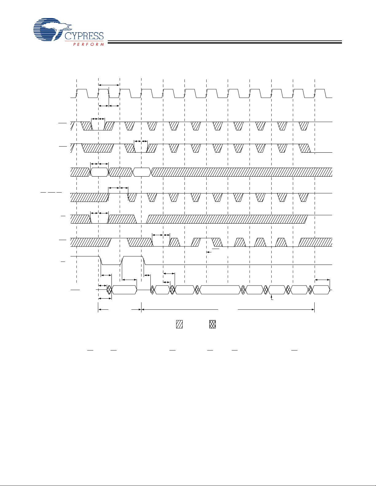
Timing Diagrams
G
Read Cycle Timing
[16]
t
CYC
CY7C1297H
CLK
ADSP
ADSC
ADDRESS
W, BWE,BW
[A:B]
CE
ADV
OE
Data Out (Q)
t
ADS
t
AS
t
CES
High-Z
t
t
CL
CH
t
ADH
t
t
ADH
ADS
t
AH
A1
t
WES
t
CEH
t
OEV
t
CLZ
Q(A1)
t
CDV
t
WEH
t
OEHZ
A2
t
t
ADVH
ADVS
t
DOH
t
CDV
t
OELZ
Q(A2) Q(A2 + 1) Q(A2 + 2)
Single READ BURST
DON’T CARE
ADV suspends burst.
READ
UNDEFINED
Deselect Cycle
Q(A2) Q(A2 + 1) Q(A2 + 2)Q(A2 + 3)
Burst wraps around
to its initial state
t
CHZ
Note:
16.On this diagram, when CE
is LOW, CE1 is LOW, CE2 is HIGH and CE3 is LOW. When CE is HIGH, CE1 is HIGH or CE2 is LOW or CE3 is HIGH.
Document #: 38-05669 Rev. *B Page 10 of 15
[+] Feedback
Page 11

Timing Diagrams (continued)
D
Write Cycle Timing
[16, 17]
t
CYC
CY7C1297H
ADSP
ADSC
ADDRESS
BWE,
BW
[A:B]
GW
CLK
CE
t
t
CL
CH
t
t
ADH
ADS
t
t
ADH
ADS
t
t
AH
AS
A1
A2 A3
Byte write signals are ignored for first cycle when
ADSP initiates burst.
t
t
CEH
CES
t
WES
t
WEH
ADSC extends burst.
t
ADS
t
ADH
t
WES
t
ADVS
t
WEH
t
ADVH
ADV
ADV suspends burst.
OE
t
t
DH
DS
Data in (D)
High-Z
t
OEHZ
D(A1)
D(A2) D(A2 + 1) D(A2 + 1)
D(A2 + 2)
D(A3) D(A3 + 1) D(A3 + 2)D(A2 + 3)
ata Out (Q)
BURST READ BURST WRITE
Single WRITE
Extended BURST WRITE
DON’T CARE UNDEFINED
Note:
17.
Full width Write can be initiated by either GW
Document #: 38-05669 Rev. *B Page 11 of 15
LOW; or by GW HIGH, BWE LOW and BW
[A:B]
LOW.
[+] Feedback
Page 12

Timing Diagrams (continued)
t
Read/Write Timing
[16, 18, 19]
CYC
CY7C1297H
CLK
ADSP
ADSC
ADDRESS
BWE, BW[A:B]
CE
ADV
OE
Data In (D)
Data Out (Q)
t
t
CL
CH
t
t
ADH
ADS
t
t
AH
AS
t
CES
A2
t
CEH
A1 A5 A6
High-Z
Q(A1)
Q(A2)
A3 A4
t
OEHZ
t
WES
t
DS
D(A3)
t
t
DH
WEH
t
OELZ
t
CDV
Q(A4) Q(A4+1) Q(A4+2) Q(A4+3)
D(A5) D(A6)
Single WRITE
BURST READBack-to-Back READs
Back-to-Back
WRITEs
Notes:
18.The data bus (Q) remains in High-Z following a Write cycle unless an ADSP
is HIGH.
19.GW
DON’T CARE UNDEFINED
, ADSC, or ADV cycle is performed.
Document #: 38-05669 Rev. *B Page 12 of 15
[+] Feedback
Page 13

Timing Diagrams (continued)
A
ZZ Mode Timing
[20, 21]
CLK
CY7C1297H
t
ZZ
t
ZZREC
I
SUPPLY
LL INPUTS
ZZ
t
ZZI
I
DDZZ
t
RZZI
DESELECT or READ Only
(except ZZ)
Outputs (Q)
High-Z
DON’T CARE
Notes:
20.Device must be deselected when entering ZZ mode. See Cycle Descriptions table for all possible signal conditions to deselect the device.
21.DQs are in High-Z when exiting ZZ sleep mode.
Document #: 38-05669 Rev. *B Page 13 of 15
[+] Feedback
Page 14

CY7C1297H
Ordering Information
Not all of the speed, package and temperature ranges are available. Please contact your local sales representative or
Speed
(MHz) Ordering Code
100 CY7C1297H-100AXC 51-85050 100-pin Thin Quad Flat Pack (14 x 20 x 1.4 mm) Lead-Free Commercial
CY7C1297H-100AXI Industrial
133 CY7C1297H-133AXC 51-85050 100-pin Thin Quad Flat Pack (14 x 20 x 1.4 mm) Lead-Free Commercial
CY7C1297H-133AXI Industrial
Package Diagram
visit www.cypress.com for actual products offered.
Package
Diagram Package Type
100-Pin TQFP (14 x 20 x 1.4 mm) (51-85050)
16.00±0.20
14.00±0.10
100
1
81
80
0.30±0.08
Operating
Range
1.40±0.05
GAUGE PLANE
R 0.08 MIN.
0.20 MAX.
0.25
0°-7°
0.60±0.15
1.00 REF.
20.00±0.10
22.00±0.20
30
31 50
0° MIN.
R 0.08 MIN.
0.20 MAX.
0.20 MIN.
A
DETAIL
0.65
TYP.
51
STAND-OFF
0.05 MIN.
0.15 MAX.
12°±1°
(8X)
SEATING PLANE
NOTE:
1. JEDEC STD REF MS-026
2. BODY LENGTH DIMENSION DOES NOT INCLUDE MOLD PROTRUSION/END FLASH
MOLD PROTRUSION/END FLASH SHALL NOT EXCEED 0.0098 in (0.25 mm) PER SIDE
BODY LENGTH DIMENSIONS ARE MAX PLASTIC BODY SIZE INCLUDING MOLD MISMATCH
3. DIMENSIONS IN MILLIMETERS
51-85050-*B
SEE DETAIL
0.20 MAX.
1.60 MAX.
0.10
A
Document #: 38-05669 Rev. *B Page 14 of 15
© Cypress Semiconductor Corporation, 2006. The information contained herein is subject to ch an ge wi t hou t n oti ce. C ypr ess S em icon duct or Corpo ration assu mes no resp onsib ility for th e u se
of any circuitry other than circuitry embodied in a Cypress product. Nor does it convey or imply any license under patent or other rights. Cypress products are not warranted nor intended to be
used for medical, life support, life saving, critical control or safety applications, unless pursuant to an express written agreement with Cypress. Fu rthermore, Cypr ess does not aut horize its
products for use as critical components in life-support systems where a malfunction or failure may reasonably be expected to result in significant injury to the user. The inclusion of Cypress
products in life-support systems application implies that the manufacturer assumes all risk of such use and in doing so indemnifies Cypress against all charges.
[+] Feedback
Page 15

CY7C1297H
Document History
Document Title: CY7C1297H 1-Mbit (64K x 18) Flow-Through Sync SRAM
Document Number: 38-05669
REV. ECN NO. Issue Date
** 345879 See ECN PCI New Data Sheet
*A 430677 See ECN NXR Changed address of Cypress Semiconductor Corporation on Page# 1 from
*B 482139 See ECN VKN Converted from Preliminary to Final.
Orig. of
Change Description of Change
“3901 North First Street” to “198 Champion Court”
Added 2.5VI/O option
Changed Three-State to Tri-State
Included Maximum Ratings for V
Modified “Input Load” to “Input Leakage Current except ZZ and MODE” in the
relative to GND
DDQ
Electrical Characteristics Table
Modified test condition from V
Replaced Package Name column with Package Diagram in the Ordering
IH
< V
DD to VIH
< V
Information table
Updated the Ordering Information table.
DD
Document #: 38-05669 Rev. *B Page 15 of 15
[+] Feedback
 Loading...