

Page 1
CY7C1146V18, CY7C1157V18
CY7C1148V18, CY7C1150V18
18-Mbit DDR-II+ SRAM 2-Word Burst
Architecture (2.0 Cycle Read Latency)
Features
Note
1. The QDR consortium specification for V
DDQ
is 1.5V + 0.1V . The Cyp ress QDR devices exceed th e QDR consorti um specifi catio n and ar e capab le of support ing V
DDQ
= 1.4V to V
DD
.
Functional Description
■ 18 Mbit density (2M x 8, 2M x 9, 1M x 18, 512K x 36)
■ 300 MHz to 375 MHz clock for high bandwidth
■ 2-Word burst for reducing address bus frequency
■ Double Data Rate (DDR) interfaces
(data transferred at 750 MHz) at 375 MHz
■ Read latency of 2.0 clock cycles
■ Two input clocks (K and K) for precise DDR timing
❐ SRAM uses rising edges only
■ Echo clocks (CQ and CQ) simplify data capture in high-speed
systems
■ Data valid pin (QVLD) to indicate valid data on the output
■ Synchronous internally self-timed writes
■ Core V
■ HSTL inputs and Variable drive HSTL output buffers
■ Available in 165-Ball FBGA p ackage (13 x 15 x 1.4 mm)
■ Offered in both Pb-free and non Pb-free packages
■ JTAG 1149.1-compatible test access port
■ Delay Lock Loop (DLL) for accurate data placement
= 1.8V ± 0.1V; IO V
DD
= 1.4V to V
DDQ
DD
[1]
Configurations
With Read Cycle Latency of 2.0 cycles:
CY7C1146V18 – 2M x 8
CY7C1157V18 – 2M x 9
CY7C1148V18 – 1M x 18
CY7C1150V18 – 512K x 36
The CY7C1146V18, CY7C1157V18, CY7C1148V18, and
CY7C1150V18 are 1.8V Synchronous Pipelined SRAMs
equipped with DDR-II+ architecture. The DDR-II+ consists of an
SRAM core with advanced synchronous peripheral circuitry.
Addresses for read and write are latched on alternate rising
edges of the input (K) clock. Write data is registered on the rising
edges of both K and K
of K and K
. Each address location is associated with two 8-bit
. Read data is driven on the rising edges
words (CY7C1146V18) or 9-bit words (CY7C1157V18) or 18-bit
words (CY7C1148V18) or 36-bit words (CY7C1150V18) that
burst sequentially into or out of the device.
Asynchronous inputs include output impedance matching input
(ZQ). Synchronous data outputs (Q, sharing the same physical
pins as the data inputs D) are tightly matched to the two output
echo clocks CQ/CQ
, eliminating the need for separately
capturing data from each individual DDR SRAM in the system
design.
All synchronous inputs pass through input registers controlled by
the K or K
registers controlled by the K or K
input clocks. All data outputs pass through output
input clocks. Writes are
conducted with on-chip synchronous self-timed write circuitry.
Selection Guide
Maximum Operating Frequency 375 333 300 MHz
Maximum Operating Current 1020 920 850 mA
Cypress Semiconductor Corporation • 198 Champion Court • San Jose, CA 95134-1709 • 408-943-2600
Document Number: 001-06621 Rev. *D Revised March 06, 2008
Description 375 MHz 333 MHz 300 MHz Unit
[+] Feedback [+] Feedback
Page 2
CY7C1146V18, CY7C1157V18
CY7C1148V18, CY7C1150V18
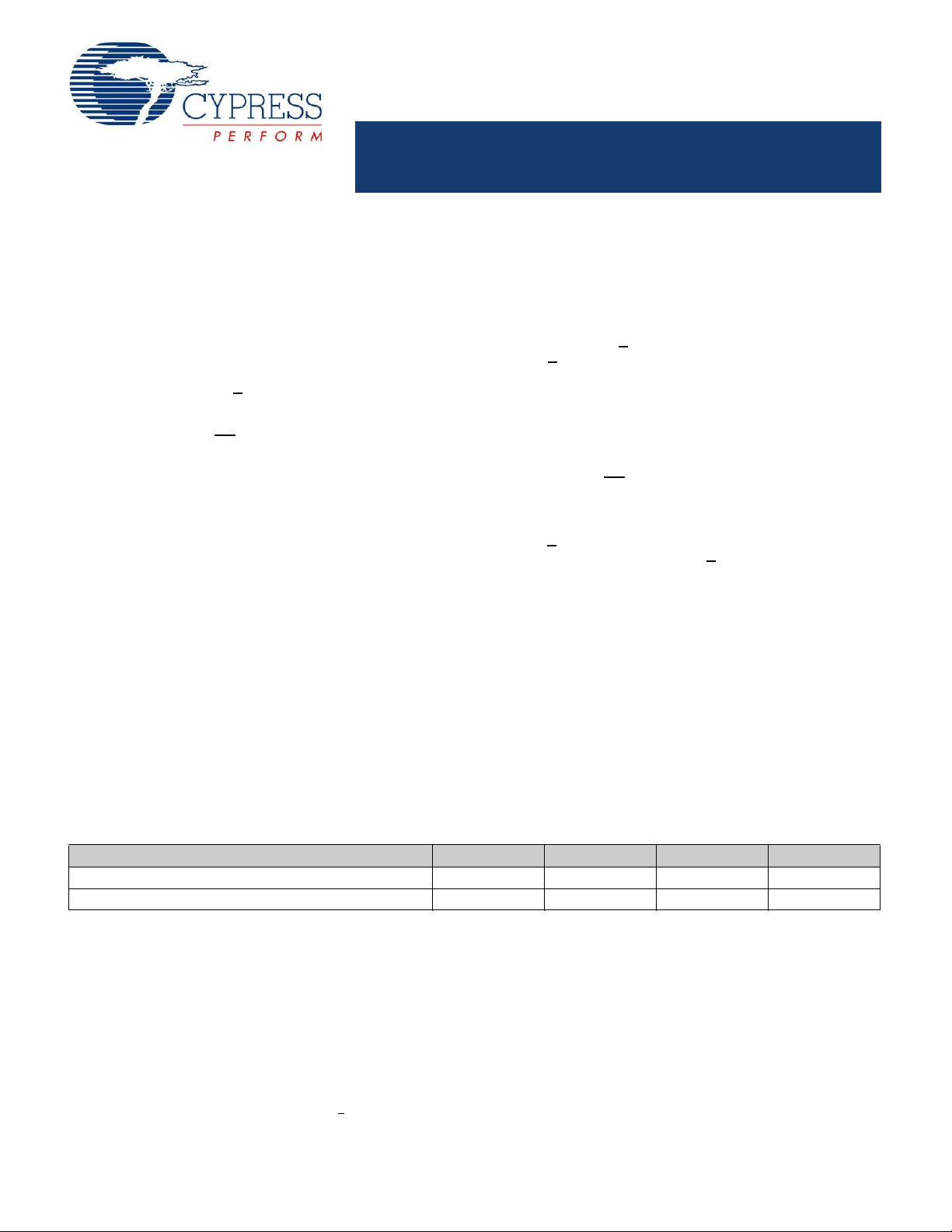
Logic Block Diagram (CY7C1146V18)
CLK
A
(19:0)
Gen.
K
K
Control
Logic
Address
Register
Read Add. Decode
Read Data Reg.
R/W
DQ
[7:0]
Output
Logic
Reg.
Reg.
Reg.
8
8
16
8
NWS
[1:0]
V
REF
Write Add. Decode
8
8
LD
Control
20
1M x 8 Array
1M x 8 Array
Write
Reg
Write
Reg
CQ
CQ
R/W
DOFF
QVLD
8
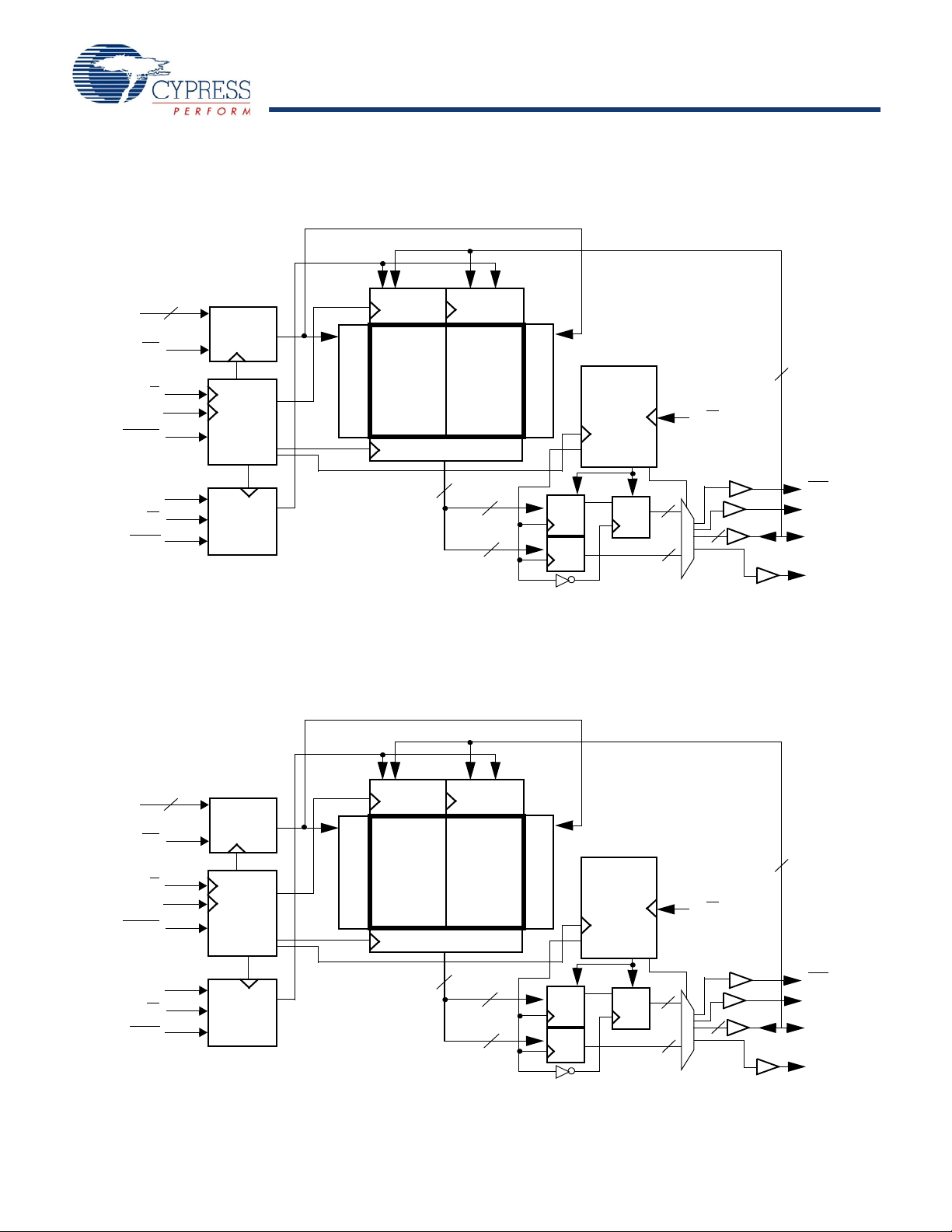
CLK
A
(19:0)
Gen.
K
K
Control
Logic
Address
Register
Read Add. Decode
Read Data Reg.
R/W
DQ
[8:0]
Output
Logic
Reg.
Reg.
Reg.
9
9
18
9
BWS
[0]
V
REF
Write Add. Decode
9
9
LD
Control
20
1M x 9 Array
1M x 9 Array
Write
Reg
Write
Reg
CQ
CQ
R/W
DOFF
QVLD
9
Logic Block Diagram (CY7C1157V18)
Document Number: 001-06621 Rev. *D Page 2 of 27
[+] Feedback [+] Feedback
Page 3
CY7C1146V18, CY7C1157V18
CY7C1148V18, CY7C1150V18
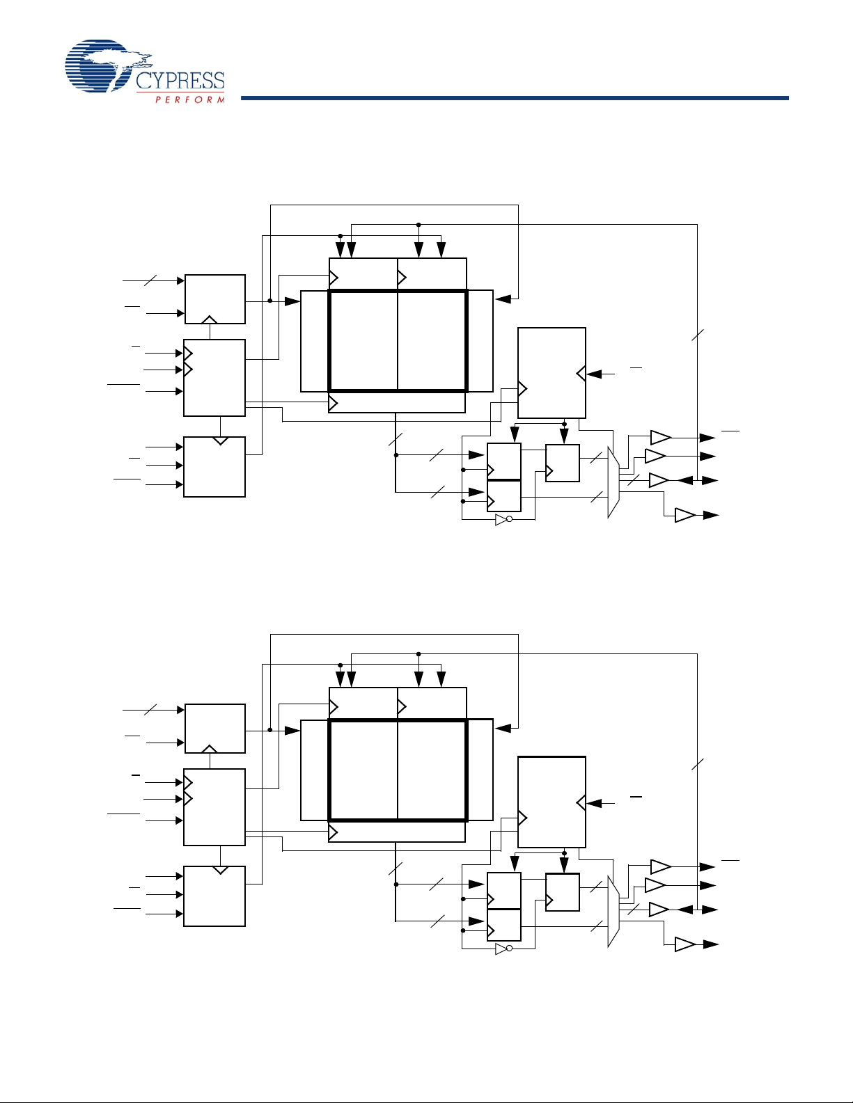
Logic Block Diagram (CY7C1148V18)
CLK
A
(18:0)
Gen.
K
K
Control
Logic
Address
Register
Read Add. Decode
Read Data Reg.
R/W
DQ
[17:0]
Output
Logic
Reg.
Reg.
Reg.
18
18
36
18
BWS
[1:0]
V
REF
Write Add. Decode
18
18
LD
Control
19
512K x 18 Array
512K x 18 Array
Write
Reg
Write
Reg
CQ
CQ
R/W
DOFF
QVLD
18
CLK
A
(17:0)
Gen.
K
K
Control
Logic
Address
Register
Read Add. Decode
Read Data Reg.
R/W
DQ
[35:0]
Output
Logic
Reg.
Reg.
Reg.
36
36
72
36
BWS
[3:0]
V
REF
Write Add. Decode
36
36
LD
Control
18
256K x 36 Array
256K x 36 Array
Write
Reg
Write
Reg
CQ
CQ
R/W
DOFF
QVLD
36
Logic Block Diagram (CY7C1150V18)
Document Number: 001-06621 Rev. *D Page 3 of 27
[+] Feedback [+] Feedback
Page 4
CY7C1146V18, CY7C1157V18
CY7C1148V18, CY7C1150V18
Pin Configurations
CY7C1146V18 (2M x 8)
165-Ball FBGA (13 x 15 x 1.4 mm) Pinout
234 5671
A
B
C
D
E
F
G
H
J
K
L
M
N
P
R
A
CQ
NC
NC
NC
NC
DOFF
NC
NC/72M A
NWS
1
KR/W
NC/144M
NC
NC
NC
NC
NC
TDO
NC
NC
NC
NC
NC
NC
TCK
NC
NC
A NC/288M
K
NWS
0
V
SS
AAA
NC V
SS
V
SS
V
SS
V
SS
V
DD
A
V
SS
V
SS
V
SS
V
DD
DQ4
NC
V
DDQ
NC
NC
NC
NC
DQ7
A
V
DDQ
V
SS
V
DDQ
V
DD
V
DD
DQ5 V
DDQ
V
DD
V
DDQ
V
DD
V
DDQ
V
DD
V
SS
V
DD
V
DDQ
V
DDQ
V
SS
V
SS
V
SS
V
SS
A
A
NC
V
SS
A
A
A
NC V
SS
NC V
SS
NC
NC
V
REF
V
SS
V
DD
V
SS
V
SS
A
V
SS
QVLD
NC
DQ6
NC
NC
NC
V
DD
A
891011
NC
A NC/36M
LD
CQ
A NC
NC
DQ3
V
SS
NC NC NC
NC
V
SS
NC
DQ2
NC
NC
NC
V
REF
NC
NC
V
DDQ
NC
V
DDQ
NC NC
V
DDQ
V
DDQ
V
DDQ
NCV
DDQ
NC
DQ1
NC
V
DDQ
V
DDQ
NC
V
SS
NC NC
NC
TDITMS
V
SS
A
NC
A
NC
NC
NC
ZQ
NC
DQ0
NC
NC
NC
NC
A
CY7C1157V18 (2M x 9)
234 5671
A
B
C
D
E
F
G
H
J
K
L
M
N
P
R
A
CQ
NC
NC
NC
NC
DOFF
NC
NC/72M A NC
K
R/W
NC/144M
NC
NC
NC
NC
NC
TDO
NC
NC
NC
NC
NC
NC
TCK
NC
NC
A NC/288M
K
BWS
0
V
SS
AAA
NC V
SS
V
SS
V
SS
V
SS
V
DD
A
V
SS
V
SS
V
SS
V
DD
DQ4
NC
V
DDQ
NC
NC
NC
NC
DQ7
A
V
DDQ
V
SS
V
DDQ
V
DD
V
DD
DQ5 V
DDQ
V
DD
V
DDQ
V
DD
V
DDQ
V
DD
V
SS
V
DD
V
DDQ
V
DDQ
V
SS
V
SS
V
SS
V
SS
A
A
NC
V
SS
A
A
A
NC V
SS
NC V
SS
NC
NC
V
REF
V
SS
V
DD
V
SS
V
SS
A
V
SS
QVLD
NC
DQ6
NC
NC
NC
V
DD
A
891011
DQ8
A NC/36M
LD
CQ
A NC
NC
DQ3
V
SS
NC NC NC
NC
V
SS
NC
DQ2
NC
NC
NC
V
REF
NC
NC
V
DDQ
NC
V
DDQ
NC NC
V
DDQ
V
DDQ
V
DDQ
NCV
DDQ
NC
DQ1
NC
V
DDQ
V
DDQ
NC
V
SS
NC NC
NC
TDITMS
V
SS
A
NC
A
NC
NC
NC
ZQ
NC
DQ0
NC
NC
NC
NC
A
Document Number: 001-06621 Rev. *D Page 4 of 27
[+] Feedback [+] Feedback
Page 5
CY7C1146V18, CY7C1157V18
CY7C1148V18, CY7C1150V18
Pin Configurations (continued)
CY7C1148V18 (1M x 18)
165-Ball FBGA (13 x 15 x 1.4 mm) Pinout
234 5671
A
B
C
D
E
F
G
H
J
K
L
M
N
P
R
A
CQ
NC
NC
NC
NC
DOFF
NC
NC/72M A
BWS
1
K
R/W
NC/144M
DQ9
NC
NC
NC
NC
TDO
NC
NC
NC
NC
NC
NC
TCK
NC
NC
A NC/288M
K
BWS
0
V
SS
ANCA
DQ10 V
SS
V
SS
V
SS
V
SS
V
DD
A
V
SS
V
SS
V
SS
V
DD
DQ11
NC
V
DDQ
NC
DQ14
NC
DQ16
DQ17
A
V
DDQ
V
SS
V
DDQ
V
DD
V
DD
DQ13 V
DDQ
V
DD
V
DDQ
V
DD
V
DDQ
V
DD
V
SS
V
DD
V
DDQ
V
DDQ
V
SS
V
SS
V
SS
V
SS
A
A
NC
V
SS
A
A
A
NC V
SS
NC V
SS
DQ12
NC
V
REF
V
SS
V
DD
V
SS
V
SS
A
V
SS
QVLD
NC
DQ15
NC
NC
NC
V
DD
A
891011
DQ0
A NC/36M
LD
CQ
A NC
NC
DQ8
V
SS
NC DQ7 NC
NC
V
SS
NC
DQ6
NC
NC
NC
V
REF
NC
DQ3
V
DDQ
NC
V
DDQ
NC DQ5
V
DDQ
V
DDQ
V
DDQ
NCV
DDQ
NC
DQ4
NC
V
DDQ
V
DDQ
NC
V
SS
NC NC
NC
TDITMS
V
SS
A
NC
A
NC
NC
NC
ZQ
NC
DQ2
NC
DQ1
NC
NC
A
CY7C1150V18 (512K x 36)
234 5671
A
B
C
D
E
F
G
H
J
K
L
M
N
P
R
A
CQ
NC
NC
NC
NC
DOFF
NC
NC/144M NC/36M
BWS
2
K
R/W
BWS
1
DQ27
DQ18
NC
NC
NC
TDO
NC
NC
DQ31
NC
NC
NC
TCK
NC
DQ28
A
BWS
3
K
BWS
0
V
SS
ANCA
DQ19 V
SS
V
SS
V
SS
V
SS
V
DD
A
V
SS
V
SS
V
SS
V
DD
DQ20
DQ21
V
DDQ
DQ32
DQ23
DQ34
DQ25
DQ26
A
V
DDQ
V
SS
V
DDQ
V
DD
V
DD
DQ22 V
DDQ
V
DD
V
DDQ
V
DD
V
DDQ
V
DD
V
SS
V
DD
V
DDQ
V
DDQ
V
SS
V
SS
V
SS
V
SS
A
ANC
V
SS
A
A
A
DQ29 V
SS
NC V
SS
DQ30
NC
V
REF
V
SS
V
DD
V
SS
V
SS
A
V
SS
QVLD
NC
DQ33
NC
DQ35
DQ24
V
DD
A
891011
DQ0
A NC/72M
LD
CQ
A NC
NC
DQ8
V
SS
NC DQ17 DQ7
NC
V
SS
NC
DQ6
DQ14
NC
NC
V
REF
NC
DQ3
V
DDQ
NC
V
DDQ
NC DQ5
V
DDQ
V
DDQ
V
DDQ
DQ4V
DDQ
NC
DQ13
NC
V
DDQ
V
DDQ
NC
V
SS
NC DQ1
NC
TDITMS
V
SS
A
NC
A
DQ16
DQ15
NC
ZQ
DQ12
DQ2
DQ10
DQ11
DQ9
NC
A
Document Number: 001-06621 Rev. *D Page 5 of 27
[+] Feedback [+] Feedback
Page 6
CY7C1146V18, CY7C1157V18
CY7C1148V18, CY7C1150V18
Pin Definitions
Pin Name IO Pin Description
DQ
[x:0]
Input OutputSynchronous
LD Input-
Synchronous
NWS
BWS
BWS
, NWS
0
, BWS1,
0
, BWS
2
, Input-
1
Synchronous
Input-
Synchronous
3
Data Input Output Signals. Inputs are sampled on the rising edge of K and K clocks when write
operations are valid. These pins drive out the requested data when a read operation is active. Valid
data is driven out on the rising edge of both the K and K
When read access is deselected, Q
CY7C1 146V18 − DQ
CY7C1 157V18 − DQ
CY7C1 148V18 − DQ
CY7C1 150V18 − DQ
[7:0]
[8:0]
[17:0]
[35:0]
are automatically tri-stated.
[x:0]
Synchronous Load. This input is brought LOW when a bus cycle sequence is to be defined. This
definition includes address and read/write direction. All transactions operate on a burst of two data.
LD must meet the setup and hold times around edge of K.
Nibble Write Select 0, 1 − Active LOW.(CY7C1146V18 Only) Sampled on the rising edge of the K
and K
clocks when the write operation is active. It is used to select the nibble that is written into the
device NWS
All the Nibble Write Selects are sampled on the same edge as the data. Deselecting a Nibble Write
controls D
0
and NWS1 controls D
[3:0]
[7:4]
Select causes the corresponding nibble of data to be ignored and not written into the device.
Byte Write Select 0, 1, 2, and 3 − Active LOW. Sampled on the rising edge of the K and K clocks
when the Write operation is active. It is used to select the byte that is written into the device when
the current portion of the write operation is active. Bytes not written remain unaltered.
CY7C1 157V18 − BWS
CY7C1 148V18 − BWS0 controls D
CY7C1 148V18 − BWS0 controls D
controls D
All the Byte Write Selects are sampled on the same edge as the data. Deselecting a Byte Write Select
[35:27]
.
controls D
0
[8:0]
, and BWS1 controls D
[8:0]
, BWS1 controls D
[8:0]
causes the corresponding byte of data to be ignored and not written into the device.
clocks when read operations are active.
.
[17:9].
, BWS2 controls D
[17:9]
[26:18]
, and BWS3
A Input-
Synchronous
Address Inputs. Sampled on the rising edge of the K clock during active read and write operations.
These address inputs are multiplexed for both read and write operations. Internally, the device is
organized as 2M x 8 (two arrays each of1M x 8) for CY7C1146V18, 2M x 9 (two arrays each of 1M
x 9) for CY7C1157V18, 1M x 18 (two arrays each of 512K x 18) for CY7C1148V18, and 512K x 36
(two arrays each of 256K x 18) for CY7C1150V18. All the address inputs are ignored when the
appropriate port is deselected.
R/W
Input-
Synchronous
Synchronous Read/Write Input. When LD is LOW, this input designates the access type (read
when R/W
is HIGH, write when R/W is LOW) for loaded address. R/W must meet the setup and hold
times around edge of K.
QVLD Valid Output
Indicator
K Input-
Clock
K Input-
Clock
Valid Output Indicator . The Q V alid indicates valid output data. QVLD is edge aligned with CQ and
CQ
.
Positive Input Clock Input. The rising edge of K is used to capture synchronous inputs to the device
and to drive out data through Q
edge of K.
when in single clock mode. All accesses are initiated on the rising
[x:0]
Negative Input Clock Input. K is used to capture synchronous inputs being presented to the device
and to drive out data through Q
when in single clock mode.
[x:0]
CQ Clock Output Synchronous Echo Clock Outputs. This is a free running clock and is synchronized to the input
clock (K) of the DDR-II+. The timings for the echo clocks are shown in the “Switching Characteristics”
on page 22.
CQ
Clock Output
Synchronous Echo Clock Outputs. This is a free running clock and is synchronized to the input
clock (K) of the DDR-II+. The timings for the echo clocks are shown in the “Switching Characteristics”
on page 22.
ZQ Input Output Impe dance Matching Input. This input is used to tune the device outputs to the system dat a
bus impedance. CQ, CQ,
connected between ZQ and ground. Alternatively, connect this pin directly to V
the minimum impedance mode. This pin cannot be connected directly to GND or left unconnected.
and Q
output impedance are set to 0.2 x RQ, where RQ is a resistor
[x:0]
, which enables
DDQ
Document Number: 001-06621 Rev. *D Page 6 of 27
[+] Feedback [+] Feedback
Page 7
CY7C1146V18, CY7C1157V18
CY7C1148V18, CY7C1150V18
Pin Definitions (continued)
Pin Name IO Pin Description
DOFF
TDO Output TDO for JTAG.
TCK Input TCK Pin for JT AG.
TDI Input TDI Pin for JTAG.
TMS Input TMS Pin for JTAG.
NC N/A Not Connected to the Die. Tie to any voltage level.
NC/36M N/A Not Connected to the Die. Tie to any voltage level.
NC/72M N/A Not Connected to the Die. Tie to any voltage level.
NC/144M N/A Not Connected to the Die. Tie to any voltage level.
NC/288M N/A Not Connected to the Die. Tie to any voltage level.
V
REF
V
DD
V
SS
V
DDQ
Input DLL Turn Off − Active LOW . Connecting this pin to ground turns off the DLL inside the device. The
timings in the DLL turned off operation are different from those listed in this data sheet. For normal
operation, connect this pin to a pull up through a 10 KΩ or less pull up resistor. The device behaves
in DDR-I mode when the DLL is turned off. In this mode, operate the device at a frequency of up to
167 MHz with DDR-I timing.
Input-
Reference
Power Supply Power Supply Inputs to the Core of the Device.
Ground Ground for the Device.
Power Supply Power Supply Inputs for the Outputs of the Device.
Reference Volt age Input. S tatic input used to set the reference level for HSTL inputs, Outputs, and
AC measurement points.
Document Number: 001-06621 Rev. *D Page 7 of 27
[+] Feedback [+] Feedback
Page 8

CY7C1146V18, CY7C1157V18
CY7C1148V18, CY7C1150V18
Functional Overview
The CY7C1146V18, CY7C1157V18, CY7C1148V18, and
CY7C1150V18 are synchronous pipelined Burst SRAMs
equipped with a DDR interface.
Accesses are initiated on the rising edge of the p ositive input
clock (K). All synchronous input and output timings refer to the
rising edge of the Input clocks (K/K).
All synchronous data inputs (D
controlled by the rising edge of the input clocks (K/K
synchronous data outputs (Q
controlled by the rising edge of the input clocks (K/K
All synchronous control (R/W, LD, BWS
input registers controlled by the rising edge of the input clock (K).
CY7C1148V18 is described in the following sections. The same
basic descriptions apply to CY7C1146V18, CY7C1157V18, and
CY7C1150V18.
Read Operations
The CY7C1148V18 is organized internally as a single array of
1M x 18. Accesses are completed in a burst of two sequential
18-bit data words. Read operations are initiated by asserting
R/W
HIGH and LD LOW at the rising edge of the positive input
clock (K). The address presented to Address inputs are stored in
the read address register. Following the next two K clock rise the
corresponding 18-bit word of data from this address location is
driven onto the Q
the subsequent rising edge of K
using K as the output timing reference. On
[17:0]
the address location generated by the burst counter is driven
onto the Q
rising edge of the input clock (K/K
. The requested data is valid 0.45 ns from the
[17:0]
each read access must be enabled to complete. Initiate read
accesses on every rising edge of the positive input clock (K).
When read access is deselected, the CY7C1148V18 first
completes the pending read transactions. Synchronous internal
circuitry automatically tri-states the outputs following the next
rising edge of the positive Input clock (K). This enables a
seamless transition between devices without the insertion of wait
states in a depth expanded memory.
Write Operations
Write operations are initiated by asserting R/W LOW and LD
LOW at the rising edge of the positive input clock (K). The
address presented to Address inputs is stored in the write
address register. On the following K clock rise the data presented
to D
provided BWS
rising edge of the Negative Input Clock (K
presented to D
provided BWS
is then written into the memory array at the specified location.
Initiate write accesses on every rising edge of the positive input
clock (K). This pipelines the data flow such that 18 bits of data
transfers into the device on every rising edge of the input clocks
(K and K
When write access is deselected, the device ignores all inputs
after the pending write operations are completed.
is latched and stored into the 18-bit Write Data register
[17:0]
are both asserted active. On the subseque nt
[1:0]
is also stored into the Write Data register
[17:0]
are both asserted active. The 36 bits of data
[1:0]
).
) pass through input registers
[x:0]
) pass through output registers
[x:0]
) inputs pass through
[0:X]
) as well.
the next 18-bit data word from
). T o maintain the internal logic,
) the information
). All
Byte Write Operations
Byte Write operations are supported by the CY7C1148V18. A
write operation is initiated as described in the Write Operations.
The bytes that are written are determined by BWS
which are sampled with each set of 18-bit data word. Asserting
and BWS
0
the appropriate Byte Write Select input when the data portion of
a write enables the data presented to be latched and written into
the device. Deasserting the Byte Write Select input when the
data portion of a write enables the data stored in the device fo r
that byte to remain unaltered. Use this feature to simplify
read/modify/write operations to a Byte Write operation.
Double Data Rate Operation
The CY7C1148V18 enables high-performance operation
through high clock frequencies (achieved through pipelining) and
double data rate mode of operation. The CY7C1148V18 requires
two No Operation (NOP) cycle when transitioning from a read to
a write cycle. At higher frequencies, some applications may
require a third NOP cycle to avoid contention.
If a read occurs after a write cycle, address and data for the write
are stored in registers. The write information must be stored
because the SRAM cannot perform the last word write to the
array without conflicting with the read. The data stays in this
register until the next write cycle occurs. On the first write cycle
after the read(s), the stored data from the earlier write is written
into the SRAM array. This is called a Posted Write.
If a Read is performed on the same address on which a write is
performed in the previous cycle, the SRAM reads out the most
current data. The SRAM does this by bypassing the memory
array and reading the data from the registers.
Depth Expansion
Depth expansion requires replicating the LD control signal for
each bank. All other control signals can be common between
banks as appropriate.
Programmable Impedance
An external resistor, RQ, must be connected between the ZQ pin
on the SRAM and V
driver impedance. The value of RQ must be 5x the value of the
to allow the SRAM to adjust its output
SS
intended line impedance driven by the SRAM. The allowable
range of RQ to guarantee impedance matching with a tolerance
of ±15% is between 175Ω and 350Ω
output impedance is adjusted every 1024 cycles upon power up
, with V
=1.5V. The
DDQ
to account for drifts in supply voltage and temperature.
Echo Clocks
Echo clocks are provided on the DDR-II+ to simplify data capture
on high-speed systems. Two echo clocks are generated by the
DDR-II+. CQ is referenced with respect to K and CQ is referenced with respect to K
. These are free-running clocks and are
synchronized to the Input clock of the DDR-II+. The timings for
the echo clocks are shown in the “Switching Characteristics” on
page 22.
Valid Data Indicator (QVLD)
QVLD is provided on the DDR-II+ to simplify data capture on high
speed systems. The QVLD is generated by the DDR-II+ device
along with Data output. This signal is also edge-aligned with the
1
Document Number: 001-06621 Rev. *D Page 8 of 27
[+] Feedback [+] Feedback
Page 9
CY7C1146V18, CY7C1157V18
CY7C1148V18, CY7C1150V18
echo clock and follows the timing of any data pin. This signal is
Notes
2. The above application shows two DDR-II+ used.
3. X = “Don’t Care,” H = Logic HIGH, L = Logic LOW,
↑ represents rising edge.
4. Device powers up deselected and the outputs in a tri-state condition.
5. “A” represents address location latched by the devices when transaction was initiated and A + 1 represents the addresses sequence in the burst.
6. “t” represents the cycle at which a Read/Write operation is started. t + 1 and t + 2 are the first and second clock cycles succeeding the “t” clock cycle.
7. Data inputs are registered at K and K
rising edges. Data outputs are delivered on K and K rising edges.
8. It is recommended that K = K
= HIGH when clock is stopped. This is not essential, but permits most rapid restart by overcoming transmission line ch arging symmetrically.
asserted half a cycle before valid data arrives.
DLL
These chips utilize a Delay Lock Loop (DLL) that is designed to
function between 120 MHz and the specified maximum clock
frequency. The DLL may be disabled by applying ground to the
DOFF
pin. When the DLL is turned off, the device behaves in
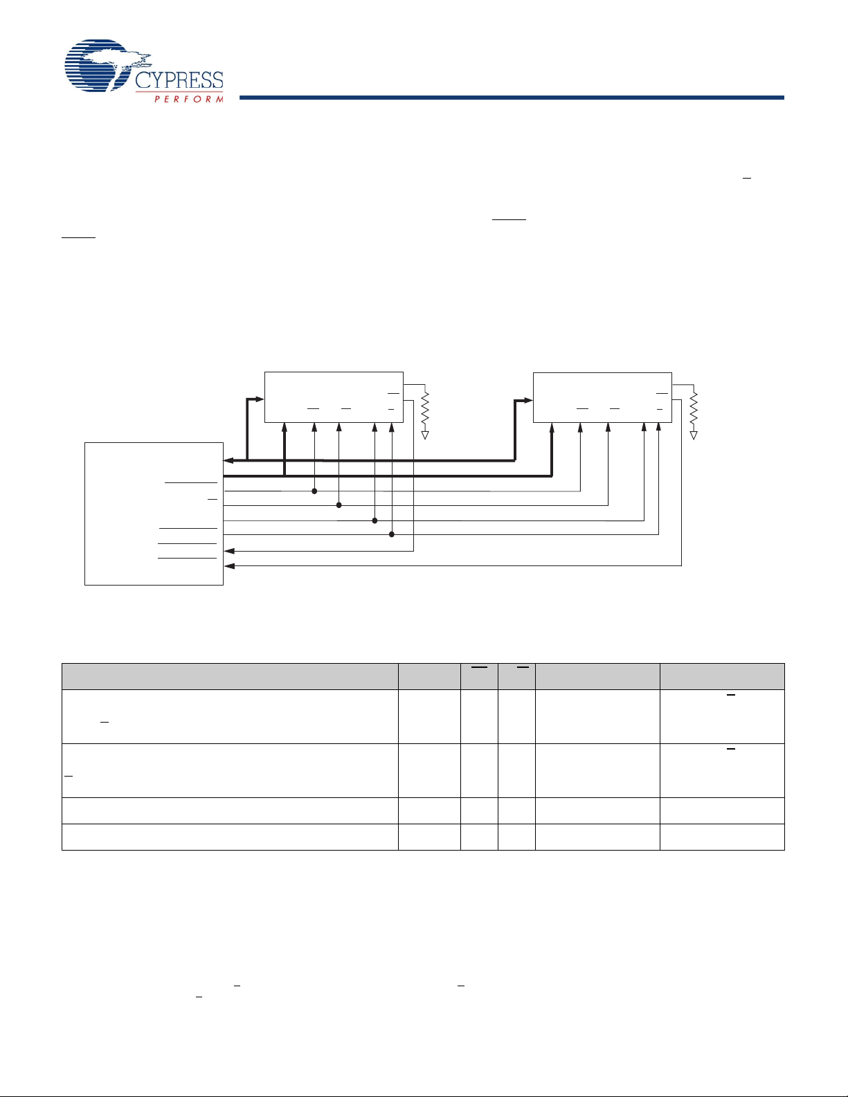
Application Example
Figure 1 shows two DDR-II+ used in an application.
Figure 1. Application Example
DDR-I mode (with 1.0 cycle latency and a longer access time).
For more information, refer to the application note, “DLL Considerations in QDRII/DDRII/QDRII+/DDRII+”. The DLL can also be
reset by slowing or stopping the input clocks K and K for a
minimum of 30 ns. However, it is not necessary for the DLL to be
reset in order to lock to the desired frequency. During Power up,
when the DOFF
is tied HIGH, the DLL gets locked after 2048
cycles of stable clock.
ZQ
CQ/CQ
K
K
R = 250ohms
DQ
A
SRAM#2
LD R/W
BUS
MASTER
(CPU or ASIC)
Echo Clock1/Echo Clock1
Echo Clock2/Echo Clock2
Addresses
Cycle Start
R/W
Source CLK
Source CLK
DQ
DQ
A
SRAM#1
LD R/W
Truth Table
The truth table for the CY7C1146V18, CY7C1157V18, CY7C1148V18, and CY7C1150V18 follows.
Operation K LD R/W DQ DQ
Write Cycle:
Load address; wait one cycle; input write data on consecutive
K and K
rising edges.
Read Cycle: (2.0 cycle latency)
Load address; wait two cycle; read data on consecutive K and
K
rising edges.
L – H L L D(A) at K (t + 1) ↑ D(A + 1) at K (t + 1) ↑
L – H L H Q(A) at K (t + 2)↑ Q(A + 1) at K
ZQ
CQ/CQ
K
K
[3, 4, 5, 6, 7, 8]
R = 250ohms
(t + 2) ↑
NOP: No Operation L – H H X High-Z High-Z
Standby: Clock Stopped Stopped X X Previous State Previous St ate
Document Number: 001-06621 Rev. *D Page 9 of 27
[+] Feedback [+] Feedback
Page 10

CY7C1146V18, CY7C1157V18
CY7C1148V18, CY7C1150V18
Write Cycle Descriptions
Note
9. Is based on a Write cycle was initiated in accordance with the Wri te Cycle Description T ruth Table. Alter BWS
0
, BWS1, BWS2, and BWS3 on different portions of a Write
cycle, as long as the setup and hold requirements are achieved.
The write cycle descriptions of CY7C1146V18 and CY7C1148V18 follows.
[3, 9]
BWS0/
NWS
0
BWS1/
NWS
K
1
K
Comments
L L L – H – When the Data portion of a write sequence is active:
CY7C1146V18 − both nibbles (D
CY7C1148V18 − both bytes (D
) are written into the device.
[7:0]
) are written into the device.
[17:0]
L L – L – H When the Data portion of a write sequence is active:
CY7C1146V18 − both nibbles (D
CY7C1148V18 − both bytes (D
) are written into the device.
[7:0]
) are written into the device.
[17:0]
L H L – H – When the Data portion of a write sequence is active:
CY7C1146V18 − only the lower nibble (D
CY7C1148V18 − only the lower byte (D
) is written into the device, D
[3:0]
) is written into the device, D
[8:0]
[7:4]
[17:9]
L H – L – H When the Data portion of a write sequence is active:
CY7C1146V18 − only the lower nibble (D
CY7C1148V18 − only the lower byte (D
) is written into the device, D
[3:0]
) is written into the device, D
[8:0]
[7:4]
[17:9]
H L L – H – When the Data portion of a write sequence is active:
CY7C1146V18 − only the upper nibble (D
CY7C1148V18 − only the upper byte (D
) is written into the device, D
[7:4]
) is written into the device, D
[17:9]
[3:0]
[8:0]
H L – L – H When the Data portion of a write sequence is active:
CY7C1146V18 − only the upper nibble (D
CY7C1148V18 − only the upper byte (D
) is written into the device, D
[7:4]
) is written into the device, D
[17:9]
[3:0]
[8:0]
H H L – H – No data is written into the devices when this portion of a write operation is active.
H H – L – H No data is written into the devices when this portion of a write operation is active.
remains unaltered.
remains unaltered.
remains unaltered.
remains unaltered.
remains unaltered.
remains unaltered.
remains unaltered.
remains unaltered.
The write cycle descriptions of CY7C1146V18 follows.
BWS
K K Comments
0
L L – H – When the Data portion of a write sequence is active, the single byte (D
L – L – H When the Data portion of a write sequence is active, the single byte (D
[3, 9]
[8:0]
[8:0]
H L – H – No data is written into th e device when this portion of a write oper a ti on is active.
H – L – H No data is written into the device when this portion of a write ope ration is active.
) is written into the device.
) is written into the device.
Document Number: 001-06621 Rev. *D Page 10 of 27
[+] Feedback [+] Feedback
Page 11

CY7C1146V18, CY7C1157V18
CY7C1148V18, CY7C1150V18
The write cycle descriptions of CY7C1148V18 follows,
[3, 9]
BWS0BWS1BWS2BWS3K K Comments
LLLLL – H–When the Data portion of a write sequence is active, all four bytes (D
written into the device.
LLLL–L – HWhen the Data portion of a write sequence is active, all four bytes (D
written into the device.
L H H H L – H – When the Data portion of a write sequence is active, only the lower byte (D
written into the device. D
remains unaltered.
[35:9]
L H H H – L – H When the Data portion of a write sequence is active, only the lower byte (D
written into the device. D
remains unaltered.
[35:9]
H L H H L – H – When the Data portion of a write sequence is active, only the byte (D
into the device. D
[8:0]
and D
remains unaltered.
[35:18]
H L H H – L – H When the Data portion of a write sequence is active, only the byte (D
into the device. D
[8:0]
and D
remains unaltered.
[35:18]
H H L H L – H – When the Data portion of a write sequence is active, only the byte (D
written into the device. D
[17:0]
and D
remains unaltered.
[35:27]
H H L H – L – H When the Data portion of a Write sequence is active, only the byte (D
written into the device. D
[17:0]
and D
remains unaltered.
[35:27]
H H H L L – H – When the Data portion of a write sequence is active, only the byte (D
written into the device. D
remains unaltered.
[26:0]
H H H L – L – H When the Data portion of a write sequence is active, only the byte (D
written into the device. D
remains unaltered.
[26:0]
[35:0]
[35:0]
[17:9]
[17:9]
[26:18]
[26:18]
[35:27]
[35:27]
) are
) are
) is
[8:0]
) is
[8:0]
) is written
) is written
) is
) is
) is
) is
HHHHL – H–No data is written into the device when this portion of a write operation is active.
HHHH–L – HNo data is written into the device when this portion of a write operation is active.
Document Number: 001-06621 Rev. *D Page 11 of 27
[+] Feedback [+] Feedback
Page 12

CY7C1146V18, CY7C1157V18
CY7C1148V18, CY7C1150V18
IEEE 1149.1 Serial Boundary Scan (JTAG)
These SRAMs incorporate a serial boundary scan test access
port (TAP) in the FBGA p ackage. This part is fully compliant with
IEEE Standard 1149.1-2001. The TAP operates using JEDEC
standard 1.8V IO logic levels.
Disabling the JTAG Feature
It is possible to operate the SRAM without using the JTAG
feature. To disable the TAP controller, TCK must be tied LOW
(VSS) to prevent clocking of the device. TDI and TMS are internally pulled up and may be unconnected. They may alternately
be connected to V
unconnected. Upon power up, the device comes up in a reset
state which does not interfere with the operation of the device.
Test Access Port—Test Clock
The test clock is used only with the TAP controller. All inputs are
captured on the rising edge of TCK. All outputs are driven from
the falling edge of TCK.
Test Mode Select
The TMS input is used to give commands to the TAP controller
and is sampled on the rising edge of TCK. It is allowable to leave
this pin unconnected if the TAP is not used. The pin is pulled up
internally, resulting in a logic HIGH level.
Test Data-In (TDI)
The TDI pin is used to serially input information into the registers
and connect to the input of any of the registers. The register
between TDI and TDO is chosen by the instruction that is loaded
into the TAP instruction register . For more information on loading
the instruction register, see the “TAP Controller State Diagram”
on page 14. TDI is internally pulled up and unconnected if the
TAP is unused in an application. TDI is connected to the most
significant bit (MSb) on any register.
Test Data-Out (TDO)
The TDO output pin is used to serially clock data out from the
registers. The output is active depending upon the curre nt state
of the TAP state machine (see Instruction codes). The output
changes on the falling edge of TCK. TDO is connected to the
least significant bit (LSB) of any register.
Performing a TAP Reset
A Reset is performed by forcing TMS HIGH (VDD) for five rising
edges of TCK. This RESET does not affect the operation of the
SRAM and may be performed while the SRAM is operating. At
power up, the TAP is reset internally to ensure that TDO comes
up in a High-Z state.
TAP Registers
Registers are connected between the TDI and TDO pins and
allow data to be scanned into and out of the SRAM test circuitry.
Select only one register at a time through the instruction
registers. Data is serially loaded into the TDI pin on the rising
edge of TCK. Data is output on the TDO pin on the falling edge
of TCK.
through a pull up resistor. TDO must be left
DD
Instruction Register
Serially load three-bit instructions into the instruction register.
This register is loaded when it is placed between the TDI and
TDO pins as shown in “TAP Controller Block Diagram” on
page 15. Upon power up, the instruction register is loaded with
the IDCODE instruction. It is also loaded with the IDCODE
instruction if the controller is placed in a reset state as described
in the previous section.
When the TAP controller is in the Capture IR state, the two least
significant bits are loaded with a binary “01” pattern to allow for
fault isolation of the board level serial test path.
Bypass Register
To save time when serially shifting data through registers, it is
sometimes advantageous to skip certain chips. The bypass
register is a single-bit register that can be placed between TDI
and TDO pins. This allows data to be shifted through the SRAM
with minimal delay. The bypass register is set LOW (V
the BYPASS instruction is executed.
Boundary Scan Register
The boundary scan register is connected to all of the input and
output pins on the SRAM. Several no connect (NC) pins are also
included in the scan register to reserve pins for higher de nsity
devices.
The boundary scan register is loaded with the contents of the
RAM Input and Output ring when the TAP controller is in the
Capture-DR state and is then placed between the TDI and TDO
pins when the controller is moved to the Shift-DR state. Use the
EXTEST, SAMPLE/PRELOAD, and SAMPLE Z instructions to
capture the contents of the Input and Output ring.
The “Boundary Scan Order” on page 18 show the order in which
the bits are connected. Each bit corresponds to one of the bumps
on the SRAM package. The MSb of the register is connected to
TDI, and the LSb is connected to TDO.
Identification (ID) Register
The ID register is loaded with a vendor-specific, 32-bit code
during the Capture-DR state when the IDCODE command is
loaded in the instruction register. The IDCODE is hardwired into
the SRAM and can be shifted out when the TAP controller is in
the Shift-DR state. The ID register has a vendor code and other
information described in the “Identification Register Definitions”
on page 17.
SS
) when
TAP Instruction Set
Eight different instructions are possible with the three-bit
instruction register. All combinations are listed in the Instruction
Code table. Three of these instructions are listed as RESERVED
and must not be used. The other five instructions are described
in detail in the following section.
Instructions are loaded into the TAP controller during the Shif t-IR
state when the instruction register is placed between TDI and
TDO. When this state is active, instructions are shifted through
the instruction register through the TDI and TDO pins. To
execute the instruction after it is shifted in, the TAP controller
needs to be moved into the Update-IR state.
Document Number: 001-06621 Rev. *D Page 12 of 27
[+] Feedback [+] Feedback
Page 13

CY7C1146V18, CY7C1157V18
CY7C1148V18, CY7C1150V18
IDCODE
The IDCODE instruction causes a vendor-specific, 32-bit code
to be loaded into the instruction register. It also places the
instruction register between the TDI and TDO pins and enable s
the IDCODE to be shifted out of the device when the TAP
controller enters the Shift-DR state. The IDCODE instruction is
loaded into the instruction register upon power up or whenever
the TAP controller is supplied a test logic reset state.
SAMPLE Z
The SAMPLE Z instruction causes the boundary scan register to
be connected between the TDI and TDO pins when the TAP
controller is in a Shift-DR state. The SAMPLE Z command puts
the output bus into a High-Z state until the next command is
supplied when the Update IR state is active.
SAMPLE/PRELOAD
SAMPLE/PRELOAD is a 1149.1 mandatory instruction. When
the SAMPLE/PRELOAD instructions are loaded into the instruction register and the TAP controller is in the Capture-DR state, a
snapshot of data on the inputs and output pins is captured in the
boundary scan register.
The user must be aware that the TAP controller clock can only
operate at a frequency up to 20 MHz, while the SRAM clock
operates more than an order of magnitude faster. Because there
is a large difference in the clock frequencies, it is possible that
when the Capture-DR state is active, an input or output undergoes a transition. The TAP may then try to capture a signal while
in transition (metastable state). This does not harm the device,
but there is no guarantee as to the value that is captured. Repeatable results may not be possible.
To guarantee that the boundary sc an register captures the correct value of a signal, the SRAM signal must be stabilized long
enough to meet the TAP controller's capture setup plus hold
times (t
correctly if there is no way in a design to stop (or slow) the clock
a SAMPLE/PRELOAD instruction. If this is an issue, it is still
possible to capture all other signals and simply ignore the value
of the CK and CK
After the data is captured, it is possible to shift out the data by
putting the TAP into the Shift-DR state. This places the boundary
scan register between the TDI and TDO pins.
and tCH). The SRAM clock input might not be captured
CS
captured in the boundary scan register.
PRELOAD enables an initial data pattern to be placed at the
latched parallel outputs of the boundary scan register cells before the selection of another boundary scan test operation.
The shifting of data for the SAMPLE and PRELOAD phases can
occur concurrently when required — that is, while data captured
is shifted out, shift in the preloaded data.
BYPASS
When the BYPASS instruction is loaded in the instruction register
and the TAP is placed in a Shift-DR state, the bypass register is
placed between the TDI and TDO pins. The advantage of the
BYPASS instruction is that it shortens the boundary scan path
when multiple devices are connected together on a board.
EXTEST
The EXTEST instruction enables the preloaded data to be driven
out through the system output pins. This instruction also selects
the boundary scan register to be connected for serial access
between the TDI and TDO in the shift-DR controller state.
EXTEST Output Bus Tri-State
IEEE Standard 1149.1 mandates that the TAP controller be able
to put the output bus into a tri-state mode.
The boundary scan register has a special bit located at bit 4 7.
When this scan cell, called the “extest output bus tri-state”, is
latched into the preload register the Update-DR state in the TAP
controller, it directly controls the state of the output (Q-bus) pins,
when the EXTEST is entered as the current instruction. When
HIGH, it enables the output buffers to drive the output bus. When
LOW, this bit places the output bus into a High-Z condition.
Set this bit by entering the SAMPLE/PRELOAD or EXTEST
command, and then shifting the desired bit into that cell, when
the Shift-DR state is active. When the Update-DR is active, the
value loaded into that shift-register cell latches into the preload
register. When the EXTEST instruction is entered, this bit directly
controls the output Q-bus pins. Note that this bit is preset HIGH
to enable the output when the device is powered u p, and also
when the TAP controller is in the Test-Logic-Reset state.
Reserved
These instructions are not implemented but are reserved for
future use. Do not use these instructions.
Document Number: 001-06621 Rev. *D Page 13 of 27
[+] Feedback [+] Feedback
Page 14
CY7C1146V18, CY7C1157V18
CY7C1148V18, CY7C1150V18
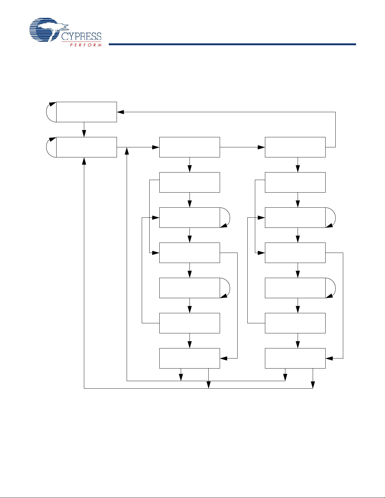
TAP Controller State Diagram
TEST-LOGIC
RESET
TEST-LOGIC/
IDLE
SELECT
DR-SCAN
CAPTURE-DR
SHIFT-DR
EXIT1-DR
PAUSE-DR
EXIT2-DR
UPDATE-DR
SELECT
IR-SCAN
CAPTURE-IR
SHIFT-IR
EXIT1-IR
PAUSE-IR
EXIT2-IR
UPDATE-IR
1
0
1
1
0
1
0
1
0
0
0
1
1
1
0
1
0
1
0
0
0
1
0
1
1
0
1
0
0
1
1
0
Note
10.The 0/1 next to each state represents the value at TMS at the rising edge of TCK.
Figure 2 shows the tap controller state diagram.
Figure 2. Tap Controller State Diagram
[10]
Document Number: 001-06621 Rev. *D Page 14 of 27
[+] Feedback [+] Feedback
Page 15

CY7C1146V18, CY7C1157V18
CY7C1148V18, CY7C1150V18
TAP Controller Block Diagram
0
012..
29
3031
Boundary Scan Register
Identification Register
012..
.
.106
012
Instruction Register
Bypass Register
Selection
Circuitry
Selection
Circuitry
TAP Controller
TDI
TDO
TCK
TMS
Notes
11.These characteristics pertain to the TAP inputs (TMS, TCK, TDI, and TDO). Parallel load levels are specified in the Electrical Characteristics Table.
12.Overshoot: V
IH
(AC) < V
DDQ
+ 0.35V (Pulse width less than t
CYC
/2), Undershoot: VIL(AC) > −0.3V (Pulse width less than t
CYC
/2).
13.All voltage referenced to ground.
Figure 3. Tap Controller Block Diagram
TAP Electrical Characteristics
The Tap Electrical Characteristics table over the operating range follows.
Parameter Description Test Conditions Min Max Unit
V
V
V
V
V
V
I
OH1
OH2
OL1
OL2
IH
IL
X
Output HIGH Voltage I
Output HIGH Voltage I
Output LOW Voltage IOL = 2.0 mA 0.4 V
Output LOW Voltage IOL = 100 μA0.2V
Input HIGH Voltage 0.65 VDDV
Input LOW Voltage –0.3 0.35 V
Input and Output Load Current GND ≤ VI ≤ V
[11, 12, 13]
= −2.0 mA 1.4 V
OH
= −100 μA1.6 V
OH
DD
+ 0.3 V
DD
DD
−55μA
V
Document Number: 001-06621 Rev. *D Page 15 of 27
[+] Feedback [+] Feedback
Page 16
CY7C1146V18, CY7C1157V18
CY7C1148V18, CY7C1150V18
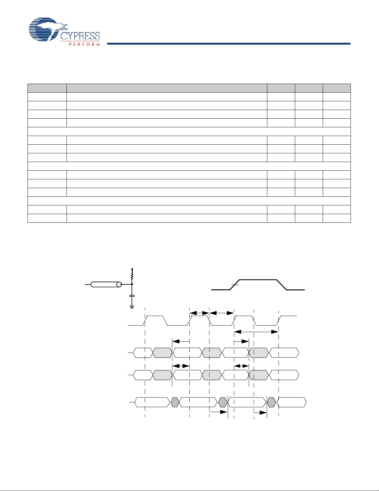
TAP AC Switching Characteristics
t
TL
t
TH
(a)
TDO
C
L
= 20 pF
Z
0
= 50
Ω
GND
0.9V
50
Ω
1.8V
0V
ALL INPUT PULSES
0.9V
Test Clock
Test Mode Select
TCK
TMS
Test Data In
TDI
Test Data Out
t
TCYC
t
TMSH
t
TMSS
t
TDIS
t
TDIH
t
TDOV
t
TDOX
TDO
Notes
14.t
CS
and tCH refer to the setup and hold time requirements of latching data from the boundary scan register.
15.Test conditions are specified using the load in TAP AC test conditions. t
R/tF
= 1 ns
The Tap AC Switching Characteristics table over the operating range follows.
Parameter Description Min Max Unit
t
TCYC
t
TF
t
TH
t
TL
TCK Clock Cycle Time 50 ns
TCK Clock Frequency 20 MHz
TCK Clock HIGH 20 ns
TCK Clock LOW 20 ns
Setup Times
t
TMSS
t
TDIS
t
CS
TMS Setup to TCK Clock Rise 5 ns
TDI Setup to TCK Clock Rise 5 ns
Capture Setup to TCK Rise 5 ns
Hold Times
t
TMSH
t
TDIH
t
CH
TMS Hold after TCK Clock Rise 5 ns
TDI Hold after Clock Rise 5 ns
Capture Hold after Clock Rise 5 ns
Output Times
t
TDOV
t
TDOX
TCK Clock LOW to TDO Valid 10 ns
TCK Clock LOW to TDO Invalid 0 ns
[14, 15]
TAP Timing and Test Condition
The Tap Timing and Test Conditions for the CY7C1146V18, CY7C1157V18, CY7C1148V18, and CY7C1150V18 follows.
Figure 4. TAP Timing and Test Conditions
[15]
Document Number: 001-06621 Rev. *D Page 16 of 27
[+] Feedback [+] Feedback
Page 17

CY7C1146V18, CY7C1157V18
CY7C1148V18, CY7C1150V18
Identification Register Definitions
Instruction Field
Revision Number
(31:29)
Cypress Device ID
(28:12)
Cypress JEDEC ID
(11:1)
ID Register
Presence (0)
CY7C1146V18 CY7C1157V18 CY7C1148V18 CY7C1150V18
000 000 000 000 Version number.
11010111100000101 110101 11100001101 11010111100010101 11010111100100101 Defines the type of
00000110100 00000110100 00000110100 00000110100 Allows unique
1 1 1 1 Indicates the
Value
Description
SRAM.
identification of
SRAM vendor.
presence of an ID
register.
Scan Register Sizes
Register Name Bit Size
Instruction 3
Bypass 1
ID 32
Boundary Scan 107
Instruction Codes
Instruction Code Description
EXTEST 000 Captures the Input Output ring contents.
IDCODE 001 Loads the ID register with the vendor ID code and places the register between TDI
SAMPLE Z 010 Captures the Input Output contents. Places the boundary scan register between TDI
RESERVED 011 Do Not Use: This instruction is reserved for future use.
SAMPLE/PRELOAD 100 Captures the Input Output ring contents. Places the boundary scan register between
RESERVED 101 Do Not Use: This instruction is reserved for future use.
RESERVED 110 Do Not Use: This instruction is reserved for future use.
BYPASS 111 Places the bypass register between TDI and TDO. This operation does not affect
and TDO. This operation does not affect SRAM operation.
and TDO. Forces all SRAM output drivers to a High-Z state.
TDI and TDO. Does not affect the SRAM operation.
SRAM operation.
Document Number: 001-06621 Rev. *D Page 17 of 27
[+] Feedback [+] Feedback
Page 18
CY7C1146V18, CY7C1157V18
CY7C1148V18, CY7C1150V18
Boundary Scan Order
Bit # Bump ID Bit # Bump ID Bit # Bump ID Bit # Bump ID
0 6R 27 11H 54 7B 81 3G
1 6P 28 10G 55 6B 82 2G
26N 299G 566A 831J
3 7P 30 11F 57 5B 84 2J
4 7N 31 11G 58 5A 85 3K
57R 329F 594A 863J
6 8R 33 10F 60 5C 87 2K
7 8P 34 11E 61 4B 88 1K
8 9R 35 10E 62 3A 89 2L
9 11P 36 10D 63 1H 90 3L
10 10P 37 9E 64 1A 91 1M
11 10N 38 10C 65 2B 92 1L
12 9P 39 11D 66 3B 93 3N
13 10M 40 9C 67 1C 94 3M
1411N 419D 681B 951N
15 9M 42 11B 69 3D 96 2M
16 9N 43 11C 70 3C 97 3P
1711L 449B 711D 982N
18 11M 45 10B 72 2C 99 2P
19 9L 46 11A 73 3E 100 1P
20 10L 47 Internal 74 2D 101 3R
2111K 489A 752E 1024R
22 10K 49 8B 76 1E 103 4P
23 9J 50 7C 77 2F 104 5P
24 9K 51 6C 78 3F 105 5N
25 10J 52 8A 79 1G 106 5R
26 11J 53 7A 80 1F
Document Number: 001-06621 Rev. *D Page 18 of 27
[+] Feedback [+] Feedback
Page 19

CY7C1146V18, CY7C1157V18
CY7C1148V18, CY7C1150V18
Power Up Sequence in DDR-II+ SRAM
K
K
Fix HIGH (tie to V
DDQ
)
VDD/V
DDQ
DOFF
Clock Start (Clock Starts after VDD/V
DDQ
is Stable)
Unstable Clock > 2048 Stable Clock
Start Normal
Operation
~
~
VDD/V
DDQ
Stable (< + 0.1V DC per 50 ns)
During Power Up, when the DOFF is tied HIGH, the D LL gets
locked after 2048 cycles of stable clock. DDR-II+ SRAMs must
be powered up and initialized in a predefined manner to prevent
undefined operations.
Power Up Sequence
■ Apply power with DOFF tied HIGH (All other inputs can be
HIGH or LOW)
❐ Apply V
❐ Apply V
■ Provide stable power and clock (K, K) for 2048 cycles to lock
the DLL.
before V
DD
before V
DDQ
DDQ
or at the same time as V
REF
REF
Power Up Waveforms
Figure 5. Power Up Waveforms
DLL Constraints
■ DLL uses K clock as its synchronizing input. The input must
have low phase jitter, which is specified as t
■ The DLL functions at frequencies down to 120 MHz.
■ If the input clock is unstable and the D LL is enabl ed, the n the
DLL may lock onto an incorrect frequency, causing unstable
SRAM behavior. T o avoid this, provide 2048 cycles stable clock
to relock to the desired clock frequency.
~
~
KC Var
.
Document Number: 001-06621 Rev. *D Page 19 of 27
[+] Feedback [+] Feedback
Page 20

CY7C1146V18, CY7C1157V18
CY7C1148V18, CY7C1150V18
Maximum Ratings
Notes
16.Power up: Is based on a linear ramp from 0V to V
DD
(min) within 200 ms. During this time V
IH
< V
DD
and V
DDQ
< VDD.
17.Outputs are impedance controlled. I
OH
= –(V
DDQ
/2)/(RQ/5) for values of 175Ω < RQ < 350Ω.
18.Outputs are impedance controlled. I
OL
= (V
DDQ
/2)/(RQ/5) for values of 175Ω < RQ < 350Ω.
19.V
REF
(min) = 0.68V or 0.46 V
DDQ
, whichever is larger, V
REF
(max) = 0.95V or 0.54 V
DDQ
, whichever is smaller.
20.The operation current is calculated with 50% read cycle and 50% write cycle.
Exceeding maximum ratings may shorten the useful life of the
device. These user guidelines are not tested.
Storage Temperature ................................ –65°C to + 150°C
Ambient Temperature with Powe r Applied –55°C to + 125°C
Supply Voltage on VDD Relative to GND.......–0.5V to + 2.9V
Supply Voltage on V
DC Applied to Outputs in High-Z .........–0.5V to V
DC Input Voltage
Relative to GND..... –0.5V to + V
DDQ
[12]
...............................–0.5V to VDD + 0.3V
DDQ
DD
+ 0.3V
Current into Outputs (LOW).........................................20 mA
Static Discharge Voltage (MIL-STD-883, M 3015).... >2001V
Latch up Current..................................................... >200 mA
Operating Range
Range
Temperature V
Commercial 0°C to +70°C 1.8 ± 0.1V 1.4V to
Industrial –40°C to +85°C
Ambient
DD
[16]
V
DDQ
V
DD
Electrical Characteristics
The DC Electrical Characteristics over the operating range follows.
Parameter Description Test Conditions Min Typ Max Unit
V
DD
V
DDQ
V
OH
V
OL
V
OH(LOW)
V
OL(LOW)
V
IH
V
IL
I
X
I
OZ
V
REF
[20]
I
DD
I
SB1
Power Supply Voltage 1.7 1.8 1.9 V
IO Supply Voltage 1.4 1.5 V
Output HIGH Voltage Note 17 V
Output LOW Voltage Note 18 V
Output HIGH Voltage IOH = –0.1 mA, Nominal Impedance V
Output LOW Voltage IOL = 0.1 mA, Nominal Impedance V
Input HIGH Voltage V
Input LOW Voltage –0.15 V
Input Leakage Current GND ≤ VI ≤ V
Output Leakage Current GND ≤ VI ≤ V
Input Reference Voltage
VDD Operating Supply V
Automatic Power Down
Current
[19]
Typical Value = 0.75V 0.68 0.75 0.95 V
= Max, I
DD
= 1/t
f = f
max
Max VDD, Both Ports
Deselected, V
V
≤ VIL f = f
IN
Inputs Static
[13]
/2 – 0.12 V
DDQ
/2 – 0.12 V
DDQ
– 0.2 V
DDQ
SS
+ 0.1 V
REF
DDQ
Output Disabled –2 2 μA
DDQ,
OUT
CYC
= 0 mA,
300 MHz 850 mA
333 MHz 920 mA
–2 2 μA
/2 + 0.12 V
DDQ
/2 + 0.12 V
DDQ
0.2 V
DDQ
REF
375 MHz 1020 mA
300 MHz 250 mA
≥ VIH or
IN
max
= 1/t
333 MHz 260 mA
,
CYC
375 MHz 290 mA
DD
DDQ
+ 0.15 V
– 0.1 V
[16]
V
V
AC Input Requirements
[12]
Over the operating range
Parameter Description Test Conditions Min Typ Max Unit
V
IH
V
IL
Document Number: 001-06621 Rev. *D Page 20 of 27
Input HIGH Voltage V
Input LOW Voltage –0.24 – V
+ 0.2 – V
REF
+ 0.24 V
DDQ
– 0.2 V
REF
[+] Feedback [+] Feedback
Page 21

CY7C1146V18, CY7C1157V18
CY7C1148V18, CY7C1150V18
Capacitance
1.25V
0.25V
R = 50Ω
5pF
INCLUDING
JIG AND
SCOPE
ALL INPUT PULSES
DEVICE
R
L
= 50Ω
Z
0
= 50Ω
V
REF
= 0.75V
V
REF
= 0.75V
[21]
0.75V
UNDER
TEST
0.75V
DEVICE
UNDER
TEST
OUTPUT
0.75V
V
REF
V
REF
OUTPUT
ZQ
ZQ
(a)
SLEW RATE= 2 V/ns
RQ =
250
Ω
(b)
RQ =
250
Ω
Note
21.Unless otherwise noted, test conditions are based upon a signal transition time of 2V/ns, timing reference levels of 0.75V, V
REF
= 0.75V, RQ = 250Ω, V
DDQ
= 1.5V,
input pulse levels of 0.25V to 1.25V, and output loading of the specified I
OL/IOH
and load capacitance shown in (a) of AC Test Loads.
Tested initially and after any design or process change that may affect these parameters.
Parameter Description Test Conditions Max Unit
Input Capacitance TA = 25°C, f = 1 MHz,
C
IN
C
CLK
C
O
Clock Input Capacitance 6 pF
Output Capacitance 7pF
V
V
= 1.8V
DD
DDQ
= 1.5V
5pF
Thermal Resistance
Tested initially and after any design or process change that may affect these parameters.
Parameter Description Test Conditions
Θ
JA
Θ
JC
Thermal Resistance
(junction to ambient)
Thermal Resistance
(junction to case)
Test conditions follow standard test methods and
procedures for measuring thermal impedance, in
accordance with EIA/JESD51.
AC Test Loads and Waveforms
Figure 6. AC Test loads and Waveforms
165 FBGA
Package
17.2 °C/W
4.15 °C/W
Unit
Document Number: 001-06621 Rev. *D Page 21 of 27
[+] Feedback [+] Feedback
Page 22

CY7C1146V18, CY7C1157V18
CY7C1148V18, CY7C1150V18
Switching Characteristics
Notes
22.When a part with a maximum frequency above 300 MHz is operating at a lower clock frequency, it requires th e input timings of the freque ncy range in which it is bei ng
operated and outputs data with the output timings of that fre quency range.
23.This part has a voltage regulator internally; t
POWER
is the time that the power needs to be supplied above V
DD
minimum initially before a read or write operation can
be initiated.
24.These parameters are extrapolated from the input timing parameters (t
KHKH
– 250 ps, where 250 ps is the internal jitter. An input jitter of 200 ps (t
KC Var
) is already
included in the t
KHKH
). These parameters are only guaranteed by design and are not tested in production.
25.t
CHZ
, t
CLZ
, are specified with a load capacitance of 5 pF as in (b) of AC Test Loads. Transition is measured ± 100 mV from steady-state voltage.
26.At any voltage and temperature t
CHZ
is less than t
CLZ
and t
CHZ
less than tCO.
27.t
QVLD
spec is applicable for both rising and falling edges of QVLD signal.
28.Hold to >V
IH
or <VIL.
Over the operating range
Cypress
Parameter
t
POWER
t
CYC
t
KH
t
KL
t
KHKH
Consortium
Parameter
t
KHKH
t
KHKL
t
KLKH
t
KHKH
Setup Times
t
SA
t
SC
t
SCDDR
t
SD
t
AVKH
t
IVKH
t
IVKH
t
DVKH
Hold Times
t
HA
t
HC
t
HCDDR
t
HD
t
KHAX
t
KHIX
t
KHIX
t
KHDX
Output Times
t
CO
t
DOH
t
CCQO
t
CQOH
t
CQD
t
CQDOHtCQHQX
t
CQH
t
CQHCQHtCQHCQH
t
CHZ
t
CLZ
t
QVLD
t
CHQV
t
CHQX
t
CHCQV
t
CHCQX
t
CQHQV
t
CQHCQL
t
CHQZ
t
CHQX1
t
QVLD
DLL Timing
t
KC Var
t
KC lock
t
KC ResettKC Reset
t
KC Var
t
KC lock
[21, 22]
VDD(Typical) to the first Access
K Clock Cycle Time 2.66 8.40 3.0 8.40 3.3 8.40 ns
Input Clock (K/K) HIGH 0.425 – 0.425 – 0.425 – t
Input Clock (K/K) LOW 0.425–0.425–0.425– t
K Clock Rise to K Clock Rise (rising edge to rising edge) 1.13 – 1.28 – 1.40 – ns
Address Setup to K Clock Rise 0.4 – 0.4 – 0.4 – ns
Control Setup to K Clock Rise (LD, R/W) 0.4–0.4–0.4– ns
Double Data Rate Control Setup to Clock (K/K) Rise (BWS0,
, BWS2, BWS3)
BWS
1
D
Setup to Clock (K/K) Rise 0.28–0.28–0.28– ns
[X:0]
Address Hold after K Clock Rise 0.4 – 0.4 – 0.4 – ns
Control Hold after K Clock Rise (LD, R/W) 0.4–0.4–0.4– ns
Double Data Rate Control Hold after Clock (K/K) Rise (BWS0,
BWS
, BWS2, BWS3)
1
D
Hold after Clock (K/K) Rise 0.28–0.28–0.28– ns
[X:0]
K/K Clock Rise to Data Valid – 0.45 – 0.45 – 0.45 ns
Data Output Hold after K/K Clock Rise (Active to Active) –0.45 – –0.45 – –0.45 – ns
K/K Clock Rise to Echo Clock Valid – 0.45 – 0.45 – 0.45 ns
Echo Clock Hold after K/K Clock Rise –0.45 – –0.45 – –0.45 – ns
Echo Clock High to Data Valid – 0.2 – 0.2 – 0.2 ns
Echo Clock High to Data Invalid –0.2 – –0.2 – –0.2 – ns
Output Clock (CQ/CQ) HIGH
CQ Clock Rise to CQ Clock Rise
(rising edge to rising edge)
Clock (K/K) Rise to High-Z (Active to High-Z)
Clock (K/K) Rise to Low-Z
Echo Clock High to QVLD Valid
Clock Phase Jitter – 0.20 – 0.20 – 0.20 ns
DLL Lock Time (K) 2048 – 2048 – 2048 – Cycles
K Static to DLL Reset
Description
[24]
[25, 26]
[28]
[23]
[27]
[24]
[25, 26]
375 MHz 333 MHz 300 MHz
Min Max Min Max Min Max
Unit
1–1–1–ms
CYC
CYC
0.28 – 0.28 – 0.28 – ns
0.28 – 0.28 – 0.28 – ns
0.88 – 1.03 – 1.15 – ns
0.88 – 1.03 – 1.15 – ns
–0.45–0.45–0.45ns
–0.45 – –0.45 – –0.45 – ns
–0.20 0.20 –0.20 0.20 –0.20 0.20 ns
30–30–30–ns
Document Number: 001-06621 Rev. *D Page 22 of 27
[+] Feedback [+] Feedback
Page 23
CY7C1146V18, CY7C1157V18
CY7C1148V18, CY7C1150V18
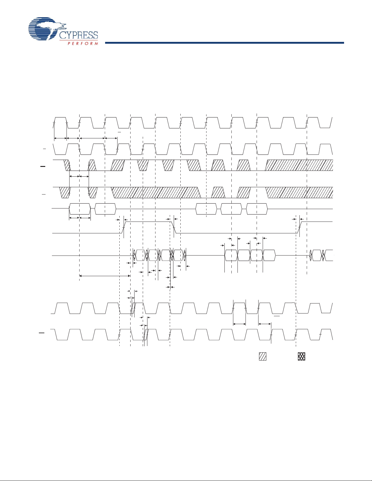
Switching Waveforms
Notes
29.Q00 refers to output from address A0. Q01 refers to output from the next internal burst address following A0, i.e., A0 + 1.
30.Outputs are disabled (High-Z) one clock cycle after a NOP.
31.The third NOP cycle between Read to Write transition is not necessary for correct device operation when Read Latency = 2.0 cycles; however at high frequency
operation, it may be required to avoid bus contention.
Read/Write/Deselect Sequence
Figure 7. Waveform for 2.0 Cycle Read Latency
[29, 30, 31]
LD
R/W
A
QVLD
DQ
NOP
1
K
t
KH
K
(Read Latency = 2.0 Cycles)
t
KL
t
t
SC
SA
READ
2
t
HC
A0
t
HA
t
CHZ
WRITE
7
A2
Q10
NOP
6
Q11
t
CQD
t
CQDOH
t
CLZ
NOP
4
Q00
t
CO
t
CCQO
t
Q01
5
QVLD
t
DOH
READ NOP WRITE
3
t
CYC
A1
t
QVLD
t
KHKH
t
CQOH
t
SD
t
HD
8
A3
D20
t
SD
D21
READ
9
A4
D30
t
HD
D31
NOP
10
t
QVLD
NOP
11
Q40
12
Q41
CQ
t
CQOH
CQ
Document Number: 001-06621 Rev. *D Page 23 of 27
t
CCQO
t
CQH
t
CQHCQH
DON’T CARE UNDEFINED
[+] Feedback [+] Feedback
Page 24

CY7C1146V18, CY7C1157V18
CY7C1148V18, CY7C1150V18
Ordering Information
Not all of the speed, package and temperature ranges are available. Contact your local sales representative or
visit www.cypress.com for actual products offered.
Speed
(MHz) Ordering Code
375 CY7C1146V18-375BZC 51-85180 165-Ball Fine Pitch Ball Grid Array (13 x 15 x 1.4 mm) Commercial
CY7C1 157V18-375BZC
CY7C1 148V18-375BZC
CY7C1 150V18-375BZC
CY7C1 146V18-375BZXC 51-85180 165-Ball Fine Pitch Ball Grid Array (13 x 15 x 1.4 mm) Pb-Free
CY7C1 157V18-375BZXC
CY7C1 148V18-375BZXC
CY7C1 150V18-375BZXC
CY7C1146V18-375BZI 51-85180 165-Ball Fine Pitch Ball Grid Array (13 x 15 x 1.4 mm) Industrial
CY7C1 157V18-375BZI
CY7C1 148V18-375BZI
CY7C1 150V18-375BZI
CY7C1 146V18-375BZXI 51-85180 165-Ball Fine Pitch Ball Grid Array (13 x 15 x 1.4 mm) Pb-Free
CY7C1 157V18-375BZXI
CY7C1 148V18-375BZXI
CY7C1 150V18-375BZXI
333 CY7C1146V18-333BZC 51-85180 165-Ball Fine Pitch Ball Grid Array (13 x 15 x 1.4 mm) Commercial
CY7C1 157V18-333BZC
CY7C1 148V18-333BZC
CY7C1 150V18-333BZC
CY7C1 146V18-333BZXC 51-85180 165-Vall Fine Pitch Ball Grid Array (13 x 15 x 1.4 mm) Pb-Free
CY7C1 157V18-333BZXC
CY7C1 148V18-333BZXC
CY7C1 150V18-333BZXC
CY7C1146V18-333BZI 51-85180 165-Ball Fine Pitch Ball Grid Array (13 x 15 x 1.4 mm) Industrial
CY7C1 157V18-333BZI
CY7C1 148V18-333BZI
CY7C1 150V18-333BZI
CY7C1 146V18-333BZXI 51-85180 165-Ball Fine Pitch Ball Grid Array (13 x 15 x 1.4 mm) Pb-Free
CY7C1 157V18-333BZXI
CY7C1 148V18-333BZXI
CY7C1 150V18-333BZXI
Package
Diagram Package Type
Operating
Range
Document Number: 001-06621 Rev. *D Page 24 of 27
[+] Feedback [+] Feedback
Page 25

CY7C1146V18, CY7C1157V18
CY7C1148V18, CY7C1150V18
Ordering Information (continued)
Not all of the speed, package and temperature ranges are available. Contact your local sales representative or
visit www.cypress.com for actual products offered.
Speed
(MHz) Ordering Code
300 CY7C1146V18-300BZC 51-85180 165-Ball Fine Pitch Ball Grid Array (13 x 15 x 1.4 mm) Commercial
CY7C1 157V18-300BZC
CY7C1 148V18-300BZC
CY7C1 150V18-300BZC
CY7C1 146V18-300BZXC 51-85180 165-Ball Fine Pitch Ball Grid Array (13 x 15 x 1.4 mm) Pb-Free
CY7C1 157V18-300BZXC
CY7C1 148V18-300BZXC
CY7C1 150V18-300BZXC
CY7C1146V18-300BZI 51-85180 165-Ball Fine Pitch Ball Grid Array (13 x 15 x 1.4 mm) Industrial
CY7C1 157V18-300BZI
CY7C1 148V18-300BZI
CY7C1 150V18-300BZI
CY7C1 146V18-300BZXI 51-85180 165-Ball Fine Pitch Ball Grid Array (13 x 15 x 1.4 mm) Pb-Free
CY7C1 157V18-300BZXI
CY7C1 148V18-300BZXI
CY7C1 150V18-300BZXI
Package
Diagram Package Type
Operating
Range
Document Number: 001-06621 Rev. *D Page 25 of 27
[+] Feedback [+] Feedback
Page 26

CY7C1146V18, CY7C1157V18
CY7C1148V18, CY7C1150V18
Package Diagram
A
1
PIN 1 CORNER
15.00±0.10
13.00±0.10
7.00
1.00
Ø0.50 (165X)
Ø0.25 M C A B
Ø0.05 M C
B
A
0.15(4X)
0.35±0.06
SEATING PLANE
0.53±0.05
0.25 C
0.15 C
PIN 1 CORNER
TOP VIEW
BOTTOM VIEW
2345678910
10.00
14.00
B
C
D
E
F
G
H
J
K
L
M
N
11
1110986754321
P
R
P
R
K
M
N
L
J
H
G
F
E
D
C
B
A
A
15.00±0.10
13.00±0.10
B
C
1.00
5.00
0.36
-0.06
+0.14
1.40 MAX.
SOLDER PAD TYPE : NON-SOLDER MASK DEFINED (NSMD)
NOTES :
PACKAGE WEIGHT : 0.475g
JEDEC REFERENCE : MO-216 / DESIGN 4.6C
PACKAGE CODE : BB0AC
51-85180-*A
Figure 8. 165-Ball FBGA (13 x 15 x 1.4 mm), 51-85180
Document Number: 001-06621 Rev. *D Page 26 of 27
[+] Feedback [+] Feedback
Page 27
CY7C1146V18, CY7C1157V18
CY7C1148V18, CY7C1150V18
Document History Page
Document Title: CY7C1146V18/CY7C1157V18/CY7C1148V18/CY7C1150V18, 18-Mbit DDR-II+ SRAM 2-Word Burst
Architecture (2.0 Cycle Read Latency)
Document Number: 001-06621
REV. ECN No. Issue Date
** 430351 See ECN NXR New data sheet
*A 461654 See ECN NXR Revised the MPNs from
*B 497629 See ECN NXR Changed the V
*C 1175245 See ECN VKN/KKVTMP Converted from preliminary to final
*D 2199066 See ECN VKN/AESA Added footnote# 20 related to I
Orig. of
Change
Description of Change
CY7C1157BV18 to CY7C1146V18
CY7C1148BV18 to CY7C1157V18
CY7C1150BV18 to CY7C1148V18
Changed t
t
from 10 ns to 5 ns and changed t
CH
Switching Characteristics table
TH
and t
from 40 ns to 20 ns, changed t
TL
, t
TMSS
from 20 ns to 10 ns in TAP AC
TDOV
TDIS
, tCS, t
Modified Power Up waveform
operating voltage to 1.4V to VDD in the Features section, in
Operating Range table and in the DC Electrical Characteristics table
DDQ
Added foot note in page 1
Changed the Maximum rating of Ambient T emperature with Power Applied from
–10°C to +85°C to –55°C to +125°C
Changed V
istics table and in the note below the table
(max) spec from 0.85V to 0.95V in the DC Electrical Character-
REF
Updated note 21 to specify Overshoot and Undershoot Spec
Updated Θ
Removed x9 part and its related information
JA
and Θ
JC
values
Updated foot note 24
Added x8 and x9 parts
Updated logic block diagram for x18 and x36 parts
Changed I
for 333 MHz, 685 mA to 850 mA for 300 MHz
values from 794 mA to 1020 mA for 375 MHz, 733 mA to 920 mA
DD
Changed ISB values from 227 mA to 290 mA for 375 MHz, 212 mA to 260 mA
for 333 MHz, 201 mA to 250 mA for 300 MHz
Changed t
Changed Θ
CYC(max)
Updated Ordering Information table
spec to 8.4 ns for all speed bins
value from 13.48 °C/W to 17.2 °C/W
JA
DD
TMSH
, t
TDIH
,
© Cypress Semiconductor Corporation, 2006- 2008. The infor mation cont ain ed herein is subj ect to change wi thout notice. C ypress Semiconductor Corporation assumes no responsibility for the use of
any circuitry other than circuitry embodied in a Cypress product. Nor does it convey or imply any license under patent or other rights. Cypress products are not warranted nor intend ed to be us ed for
medical, life support, life saving, critica l contr o l or safety applications, unless pursuant to an express wr i tte n ag reement with Cypress. Furthermore, Cypress does not authorize i t s pro ducts for use as
critical components in life-support systems where a malfunction or fa ilure may reasonably be expe cted to result in significa nt injury to the us er . The inclu sion of Cypress p roducts in life -support systems
application implies that the manufacturer assumes all risk of such use and in doing so indemnifies Cypress against all charges.
Any Source Code (software and/or firmware) is owned by Cypress Semiconductor Corporation (Cypress) and is protected by and subject to worldwide patent protection (United States and foreign),
United States copyright laws and international treaty provisions. Cypress hereby gr ant s to l icense e a pers onal, no n-exclu sive , non-tr ansfer able license to copy, use, modify, create derivative works of,
and compile the Cypress Source Code and derivative works for the sole purpose of creating custom software and or firmware in support of licensee product to be used only in conju nction with a Cypress
integrated circuit as specified in the ap plicable agreem ent. Any reprod uction, modificatio n, translation, co mpilation, or repr esentation of this Source Co de except as speci fied above is pro hibited with out
the express written permission of Cypress.
Disclaimer: CYPRESS MAKES NO WARRANTY OF ANY KIND, EXPRESS OR IMPLIED, WITH REGARD TO THIS MATERIAL, INCLUDING, BUT NOT LIMITED TO, THE IMPLIED WARRANTIES
OF MERCHANTABILITY AND FITNESS FOR A PARTICULAR PURPOSE. Cypress reserves the right to make changes without further notice to the materials described herein. Cypress d oes not
assume any liability arising out of the applic ation or use o f any pr oduct or circ uit de scribed herein . Cypr ess does n ot author ize its p roducts fo r use as critical compon ents in life-su pport systems whe re
a malfunction or failure may reason ably be expected to result in significant injury to the user. The inclusion of Cypress’ product in a life-support systems application implies that the manufacturer
assumes all risk of such use and in doing so indemnifies Cypress against all charges.
Use may be limited by and subject to the applicable Cypress software license agreement.
Document Number: 001-06621 Rev. *D Revised March 06, 2008 Page 27 of 27
QDR™ is a trademark of Cypress Semiconductor Corp. QDR RAMs and Quad Data Rate RAMs comprise a new family of products developed by Cypress, IDT, NEC, Renesas, and Samsung. All
product and company names mentioned in this document are the tradem arks of their respective holder s.
[+] Feedback [+] Feedback
 Loading...