

Page 1
CY7C106D
CY7C1006D
1-Mbit (256K x 4) Static RAM
Features
• Pin- and function-compatible with CY7C106B/CY7C1006B
• High speed
AA =
10 ns
—t
• Low active power
= 80 mA @ 10 ns
—I
CC
• Low CMOS standby power
—I
= 3.0 mA
SB2
• 2.0V Data Retention
• Automatic power-down when deselected
• CMOS for optimum speed/power
• TTL-compatible inputs and outputs
• CY7C106D available in Pb-free 28-pin 400-Mil wide Molded
SOJ package. CY7C1006D available in Pb-free 28-pin
300-Mil wide Molded SOJ package
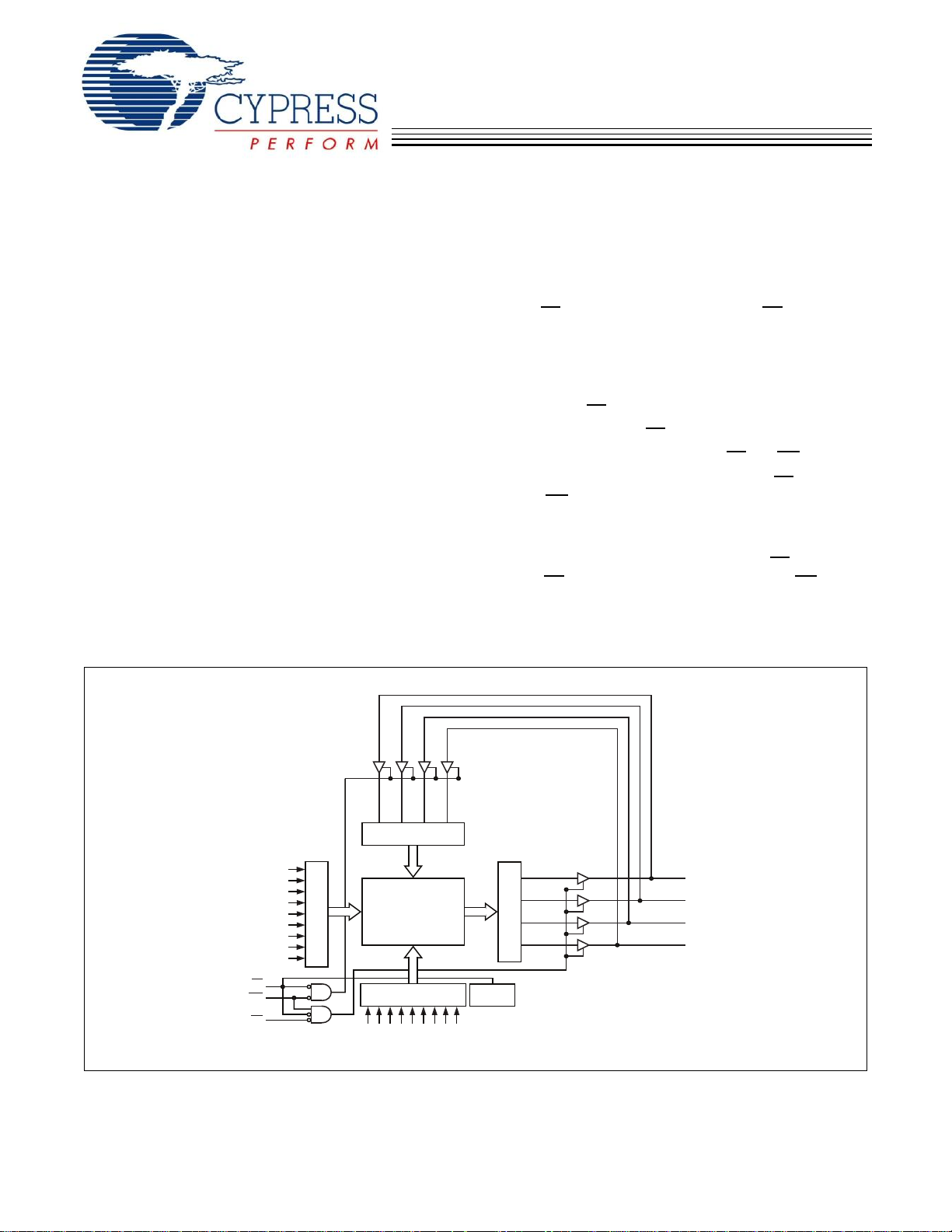
Logic Block Diagram
Functional Description
[1]
The CY7C106D and CY7C1006D are high-performance
CMOS static RAMs organized as 262,144 words by 4 bits.
Easy memory expansion is provided by an active LOW Chip
Enable (CE
), an active LOW Output Enable (OE), and tri-state
drivers. These devices have an automatic power-down feature
that reduces power consumption by more than 65% when the
devices are deselected. The four input and output pins (IO
through IO3) are placed in a high-impedance state when:
• Deselected (CE
• Outputs are disabled (OE
• When the write operation is active (CE
HIGH)
HIGH)
and WE LOW)
Write to the device by taking Chip Enable (CE) and Write
Enable (WE
) inputs LOW. Data on the four IO pins (IO
through IO3) is then written into the location specified on the
address pins (A
through A17).
0
Read from the device by taking Chip Enable (CE) and Output
Enable (OE
) LOW while forcing Write Enable (WE) HIGH.
Under these conditions, the contents of the memory location
specified by the address pins appears on the four IO pins.
0
0
INPUT BUFFER
A
1
A
2
A
3
A
4
A
5
A
6
A
7
A
A
CE
WE
OE
Note
1. For guidelines on SRAM system design, please refer to the ‘System Design Guidelines’ Cypress application note, available on the internet at www.cypress.com.
8
9
ROW DECODER
256K x 4
ARRAY
COLUMN DECODER
15
12
11
A13A14A
A
A0A10A
A16A
SENSE AMPS
POWER
DOWN
17
IO
0
IO
1
IO
2
IO
3
Cypress Semiconductor Corporation • 198 Champion Court • San Jose, CA 95134-1709 • 408-943-2600
Document #: 38-05459 Rev. *E Revised February 22, 2007
[+] Feedback
Page 2
CY7C106D
CY7C1006D
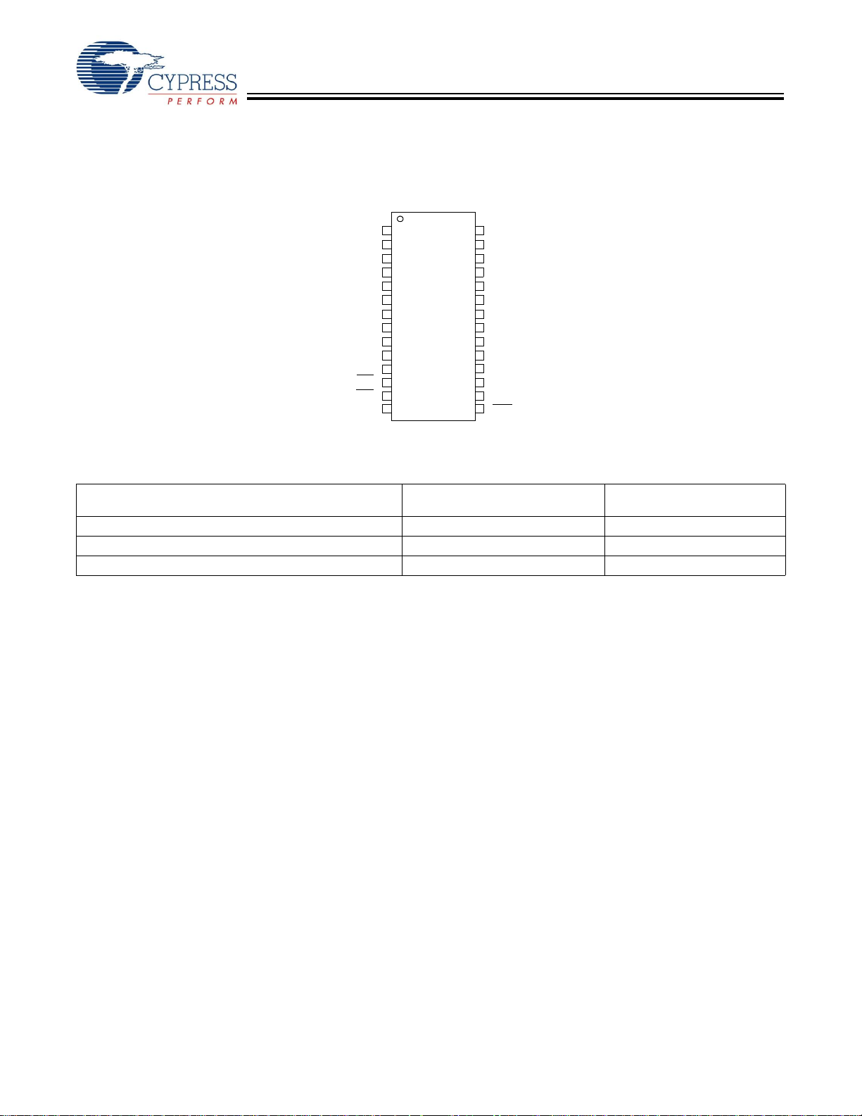
Pin Configuration
[2]
SOJ
Top View
A
A
A
A
A
A
A
A
A
A
A
CE
OE
GND
1
0
2
1
3
2
4
3
5
4
6
5
7
6
7
8
9
8
10
9
10
11
12
13
14
28
27
26
25
24
23
22
21
20
19
18
17
16
15
V
A
A
A
A
A
A
A
NC
IO
IO
IO
IO
WE
CC
17
16
15
14
13
12
11
3
2
1
0
Selection Guide
CY7C106D-10
CY7C1006D-10
Maximum Access Time 10 ns
Maximum Operating Current 80 mA
Maximum Standby Current 3 mA
Unit
Note
2. NC pins are not connected on the die.
Document #: 38-05459 Rev. *E Page 2 of 11
[+] Feedback
Page 3
CY7C106D
CY7C1006D
Maximum Ratings
Exceeding the maximum ratings may impair the useful life of
the device. These user guidelines are not tested.
Storage Temperature .................................–65°C to +150°C
Ambient Temperature with
Power Applied.............................................–55°C to +125°C
Supply Voltage on V
DC Voltage Applied to Outputs
in High-Z State
Relative to GND
CC
[3]
...................................–0.5V to VCC + 0.5V
[3]
... –0.5V to +6.0V
DC Input Voltage
Current into Outputs (LOW) ........................................ 20 mA
Static Discharge Voltage .......................................... > 2001V
(per MIL-STD-883, Method 3015)
Latch-up Current .................................................... > 200 mA
Operating Range
Range
Industrial –40°C to +85°C 5V ± 0.5V 10 ns
Electrical Characteristics (Over the Operating Range)
Parameter Description Test Conditions
V
OH
V
OL
V
IH
V
IL
I
IX
I
OZ
I
CC
Output HIGH Voltage IOH = –4.0 mA 2.4 V
Output LOW Voltage IOL = 8.0 mA 0.4 V
Input HIGH Voltage 2.2 V
Input LOW Voltage
Input Leakage Current GND < VI < V
[3]
CC
Output Leakage Current GND < VI < VCC, Output Disabled –1 +1 µA
VCC Operating Supply Current VCC = Max,
I
OUT
f = f
max
= 0 mA,
= 1/t
RC
[3]
............................... –0.5V to VCC + 0.5V
Ambient
Tem per atur e
V
CC
Speed
7C106D-10
7C1006D-10
Unit
Min Max
+ 0.5 V
CC
–0.5 0.8 V
–1 +1 µA
100 MHz 80 mA
83 MHz 72 mA
66 MHz 58 mA
I
SB1
I
SB2
Note
3. V
(min) = –2.0V and VIH(max) = VCC + 1V for pulse durations of less than 5 ns.
IL
Automatic CE Power-Down
Current—TTL Inputs
Automatic CE Power-Down
Current—CMOS Inputs
Max VCC, CE > VIH,
V
Max VCC, CE > VCC – 0.3V,
V
> VIH or VIN < VIL, f = f
IN
> VCC – 0.3V or VIN < 0.3V, f=0
IN
max
40 MHz 37 mA
10 mA
3mA
Document #: 38-05459 Rev. *E Page 3 of 11
[+] Feedback
Page 4
CY7C106D
CY7C1006D
Capacitance
[4]
Parameter Description Test Conditions Max Unit
CIN: Addresses Input Capacitance TA = 25°C, f = 1 MHz, VCC = 5.0V 7 pF
C
: Controls 10 pF
IN
C
OUT
Thermal Resistance
Parameter Description Test Conditions
Θ
JA
Θ
JC
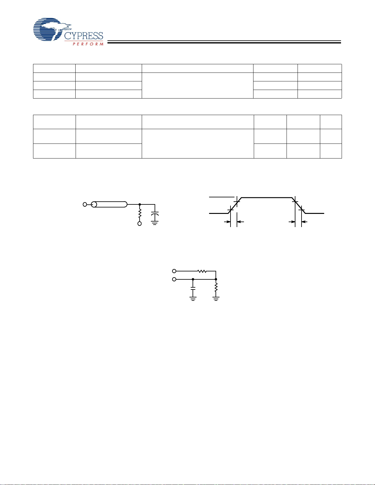
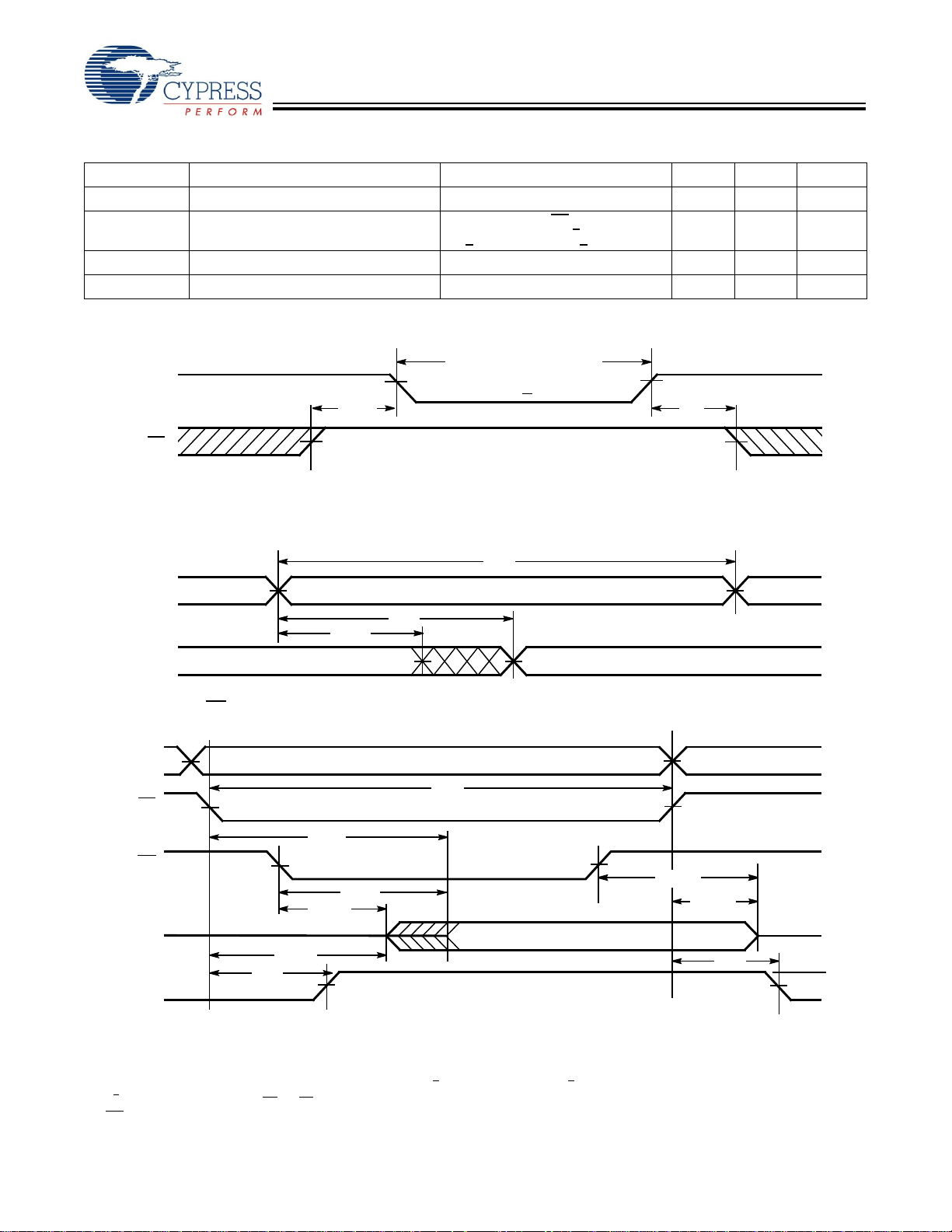
AC Test Loads and Waveforms
* CAPACITIVE LOAD CONSISTS
OF ALL COMPONENTS OF THE
TEST ENVIRONMENT
Output Capacitance 10 pF
[4]
300-Mil
Wide SOJ
Thermal Resistance
(Junction to Ambient)
Thermal Resistance
Still Air, soldered on a 3 × 4.5 inch,
four-layer printed circuit board
59.16 58.76 °C/W
40.84 40.54 °C/W
(Junction to Case)
[5]
ALL INPUT PULSES
90%
10%
(b)
OUTPUT
Z = 50
Ω
50 Ω
1.5V
30 pF*
3.0V
GND
Rise Time: ≤ 3 ns
(a)
400-Mil
Wide SOJ
90%
10%
Fall Time: ≤ 3 ns
Unit
High-Z characteristics:
5V
OUTPUT
INCLUDING
JIG AND
SCOPE
5 pF
R1 480Ω
R2
255Ω
(c)
Notes
4. Tested initially and after any design or process changes that may affect these parameters.
5. AC characteristics (except High-Z) are tested using the load conditions shown in Figure (a). High-Z characteristics are tested for all speeds using the test load
shown in Figure (c).
Document #: 38-05459 Rev. *E Page 4 of 11
[+] Feedback
Page 5

CY7C106D
CY7C1006D
Switching Characteristics (Over the Operating Range)
Parameter Description
Read Cycle
[7]
t
power
t
RC
t
AA
t
OHA
t
ACE
t
DOE
t
LZOE
t
HZOE
t
LZCE
t
HZCE
[10]
t
PU
[10]
t
PD
Write Cycle
t
WC
t
SCE
t
AW
t
HA
t
SA
t
PWE
t
SD
t
HD
t
LZWE
t
HZWE
VCC(typical) to the first access 100 µs
Read Cycle Time 10 ns
Address to Data Valid 10 ns
Data Hold from Address Change 3 ns
CE LOW to Data Valid 10 ns
OE LOW to Data Valid 5 ns
OE LOW to Low Z 0 ns
OE HIGH to High Z
CE LOW to Low Z
CE HIGH to High Z
[8, 9]
[9]
[8, 9]
CE LOW to Power-Up 0 ns
CE HIGH to Power-Down 10 ns
[11, 12]
Write Cycle Time 10 ns
CE LOW to Write End 7 ns
Address Set-Up to Write End 7 ns
Address Hold from Write End 0 ns
Address Set-Up to Write Start 0 ns
WE Pulse Width 7 ns
Data Set-Up to Write End 6 ns
Data Hold from Write End 0 ns
WE HIGH to Low Z
WE LOW to High Z
[9]
[8, 9]
[6]
7C106D-10
7C1006D-10
Unit
Min Max
5ns
3ns
5ns
3ns
5ns
Notes
6. Test conditions assume signal transition time of 3 ns or less, timing reference levels of 1.5V, input pulse levels of 0 to 3.0V, and output loading of the specified
7. t
8. t
9. At any given temperature and voltage condition, t
10. This parameter is guaranteed by design and is not tested.
11. The internal write time of the memory is defined by the overlap of CE
and 30-pF load capacitance.
I
OL/IOH
gives the minimum amount of time that the power supply should be at typical VCC values until the first memory access can be performed.
POWER
, t
HZCE
, and t
HZOE
enter a high impedance state.
can terminate the write. The input data set-up and hold timing should be referenced to the leading edge of the signal that terminates the write.
are specified with a load capacitance of 5 pF as in part (c) of “AC Test Loads and Waveforms
HZWE
is less than t
HZCE
, t
LZCE
is less than t
HZOE
and WE LOW. CE and WE must be LOW to initiate a write, and the transition of either of these signals
LZOE
, and t
HZWE
[5]
” on page 4. Transition is measured when the outputs
is less than t
for any given device.
LZWE
Document #: 38-05459 Rev. *E Page 5 of 11
[+] Feedback
Page 6
CY7C106D
CY7C1006D
Data Retention Characteristics (Over the Operating Range)
Parameter Description Conditions Min Max Unit
V
DR
I
CCDR
[4]
t
CDR
[13, 14]
t
R
Data Retention Waveform
V
Switching Waveforms
Read Cycle No.1 (Address Transition Controlled)
VCC for Data Retention 2.0 V
Data Retention Current VCC = VDR = 2.0V, CE > VCC – 0.3V,
V
> VCC – 0.3V or VIN < 0.3V
IN
Chip Deselect to Data Retention Time 0 ns
Operation Recovery Time t
DATA RETENTION MODE
CC
CE
t
CDR
[15, 16]
VDR> 2V
RC
4.5V4.5V
t
R
3mA
ns
ADDRESS
DATA OUT
PREVIOUS DATA VALID DATA VALID
Read Cycle No. 2 (OE Controlled)
ADDRESS
CE
OE
DATA OUT
V
CC
SUPPLY
CURRENT
HIGH IMPEDANCE
t
LZCE
t
PU
[16, 17]
t
ACE
t
LZOE
t
OHA
50%
t
DOE
t
RC
t
AA
t
RC
t
HZOE
t
DATA VALID
HZCE
t
PD
HIGH
IMPEDANCE
I
CC
50%
I
SB
Notes
13. Full device operation requires linear V
14. t
< 3 ns for all speeds.
r
15. Device is continuously selected, OE
16. WE
is HIGH for read cycle.
ramp from V
CC
and CE = VIL.
DR
to V
> 50 µs or stable at V
CC(min)
CC(min)
> 50 µs.
Document #: 38-05459 Rev. *E Page 6 of 11
[+] Feedback
Page 7
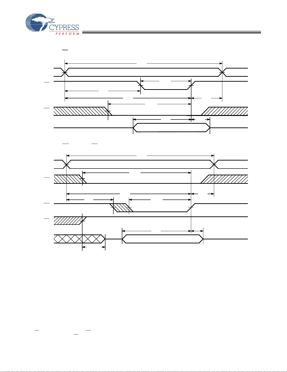
Switching Waveforms (continued)
Write Cycle No. 1 (CE
ADDRESS
CE
WE
Controlled)
[18, 19]
CY7C106D
CY7C1006D
t
WC
t
SCE
t
SA
t
AW
t
PWE
t
HA
DATA IO
Write Cycle No. 2 (WE Controlled, OE HIGH During Write)
ADDRESS
t
SCE
CE
t
AW
t
SA
WE
OE
DATA IO
t
HZOE
[18, 19]
t
WC
t
SD
DATA VALID
t
PWE
t
SD
DATA VALID
t
HD
t
HA
t
HD
Notes
18. If CE
goes HIGH simultaneously with WE going HIGH, the output remains in a high-impedance state.
19. Data IO is high impedance if OE
= VIH.
Document #: 38-05459 Rev. *E Page 7 of 11
[+] Feedback
Page 8

Switching Waveforms (continued)
Write Cycle No. 3 (WE
ADDRESS
CE
Controlled, OE LOW)
[12, 19]
t
SCE
CY7C106D
CY7C1006D
t
WC
t
HA
t
LZWE
t
HD
WE
DATA IO
t
AW
t
SA
t
HZWE
t
PWE
t
SD
DATA VALID
Truth Table
CE OE WE Input/Output Mode Power
H X X High Z Power-Down Standby (ISB)
L L H Data Out Read Active (I
CC
L X L Data In Write Active (ICC)
L H H High Z Selected, Outputs Disabled Active (ICC)
Ordering Information
Speed
(ns) Ordering Code
10 CY7C106D-10VXI 51-85032 28-pin (400-Mil) Molded SOJ (Pb-free) Industrial
CY7C1006D-10VXI 51-85031 28-pin (300-Mil) Molded SOJ (Pb-free)
Please contact your local Cypress sales representative for availability of these parts.
Package
Diagram
Package Type
)
Operating
Range
Document #: 38-05459 Rev. *E Page 8 of 11
[+] Feedback
Page 9

Package Diagrams
Figure 1. 28-pin (300-Mil) Molded SOJ, 51-85031
NOTE :
1. JEDEC STD REF MO088
2. BODY LENGTH DIMENSION DOES NOT INCLUDE MOLD PROTRUSION/END FLASH
MOLD PROTRUSION/END FLASH SHALL NOT EXCEED 0.006 in (0.152 mm) PER SIDE
3. DIMENSIONS IN INCHES
MIN.
MAX.
PIN 1 ID
114
DETAIL
EXTERNAL LEAD DESIGN
A
CY7C106D
CY7C1006D
0.050
TYP.
15 28
0.697
0.713
A
0.291
0.300
0.025 MIN.
0.120
0.140
0.330
0.350
SEATING PLANE
0.004
0.013
0.019
OPTION 1 OPTION 2
0.007
0.013
0.262
0.272
0.026
0.032
0.014
0.020
51-85031-*C
Document #: 38-05459 Rev. *E Page 9 of 11
[+] Feedback
Page 10

Package Diagrams
CY7C106D
CY7C1006D
Figure 2. 28-pin (400-Mil) Molded SOJ, 51-85032
PIN 1 I.D
114
DIMENSIONS IN INCHES
.395
.435
.445
.405
15 28
.720
.730
SEATING PLANE
.128
.148
.026
.032
.025 MIN.
0.004
.360
.380
.015
.020
All product and company names mentioned in this document may be the trademarks of their respective holders.
MIN.
MAX.
.007
.013
51-85032-*B
Document #: 38-05459 Rev. *E Page 10 of 11
© Cypress Semiconductor Corporation, 2006-2007. The information contained herein is subject to change without notice. Cypress Semiconductor Corporation assumes no responsibility for
the use of any circuitry other than circuitry embodied in a Cypress product. Nor does it convey or imply any license under patent or other rights. Cypress products are not warrant ed nor intended
to be used for medical, life support, life saving, critical control or safety applications, unless pursuant to an express written agreement with Cypress. Furthermore, Cypress does not authorize
its products for use as critical components in life-support systems where a malfunction or failure may reasonably be expected to result in significant injury to the user. The inclusion of Cypress
products in life-support systems application implies that the manufacturer assumes all risk of such use and in doing so indemnifies Cypress against all charges.
[+] Feedback
Page 11
Document History Page
Document Title: CY7C106D/CY7C1006D, 1-Mbit (256K x 4) Static RAM
Document Number: 38-05459
REV. ECN NO. Issue Date
** 201560 See ECN SWI Advance information data sheet for C9 IPP
*A 233693 See ECN RKF I
*B 262950 See ECN RKF Added T
*C See ECN See ECN RKF Reduced Speed bins to -10 and -12 ns
*D 560995 See ECN VKN Converted from Preliminary to Final
*E 802877 See ECN VKN Changed I
Orig. of
Change
Description of Change
CC,ISB1,ISB2
Pb-free offering in the ‘ordering information’
Shaded ‘Ordering Information’
Removed Commercial Operating range
Removed 12 ns speed bin
Added I
Updated Thermal Resistance table
Updated Ordering Information table
Changed Overshoot spec from V
83MHz, 45 mA to 58 mA for 66MHz, 30 mA to 37 mA for 40MHz
Specs are modified as per EROS (Spec # 01-2165)
Spec in Switching Characteristics table
power
values for the frequencies 83MHz, 66MHz and 40MHz
CC
spec from 60 mA to 80 mA for 100MHz, 55 mA to 72 mA for
CC
CY7C106D
CY7C1006D
+2V to VCC+1V in footnote #3
CC
Document #: 38-05459 Rev. *E Page 11 of 11
[+] Feedback
 Loading...