CY7C1041GN
4-Mbit (256K words × 16 bit) Static RAM
4-Mbit (256K words × 16 bit) Static RAM
Notes
1. Typical values are included only for reference and are not guaranteed or tested. Typical values are measured at V
CC
= 1.8 V (for a VCC range of 1.65 V–2.2 V),
V
CC
= 3 V (for a VCC range of 2.2 V–3.6 V), and VCC = 5 V (for a VCC range of 4.5 V–5.5 V), TA = 25 °C.
Features
Data writes are performed by asserting the Chip Enable (CE
Write Enable (WE) inputs LOW, while providing the data on I/O
■ High speed
❐ t
= 10 ns / 15 ns
AA
■ Low active and standby currents
❐ Active current: I
❐ Standby current: I
■ Operating voltage range: 1.65 V to 2.2 V, 2.2 V to 3.6 V, and
= 38-mA typical
CC
= 6-mA typical
SB2
4.5 V to 5.5 V
■ 1.0-V data retention
■ TTL-compatible inputs and outputs
■ Pb-free 44-pin SOJ, 44-pin TSOP II, and 48-ball VFBGA
packages
Functional Description
CY7C1041GN is high-performance CMOS fast static RAM
Organized as 256K words by 16-bits.
through I/O
and address on A0 through A17 pins. The Byte High
15
Enable (BHE) and Byte Low Enable (BLE) inputs control write
operations to the upper and lower bytes of the specified memory
location. BHE
controls I/O8 through I/O15 and BLE controls I/O
through I/O7.
Data reads are performed by asserting the Chip Enable (CE
Output Enable (OE) inputs LOW and providing the required
address on the address lines. Read data is accessible on the I/O
lines (I/O
through I/O15). Byte accesses can be performed by
0
asserting the required byte enable signal (BHE or BLE) to read
either the upper byte or the lower byte of data from the specified
address location.
All I/Os (I/O
through I/O15) are placed in a high-impedance state
0
during the following events:
■ The device is deselected (CE HIGH)
■ The control signals (OE, BLE, BHE) are de-asserted
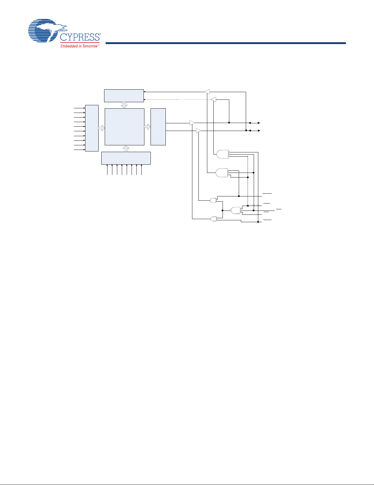
The logic block diagram is on page 2.
Product Portfolio
Power Dissipation
f = f
max
Max Typ
Product Range VCC Range (V)
CY7C1041GN18
Speed
(ns)
10/15
1.65 V–2.2 V 15 – 40
Operating ICC, (mA)
[1]
Typ
Industrial
CY7C1041GN 4.5 V–5.5 V 10 38 45
Standby, I
[1]
68CY7C1041GN30 2.2 V–3.6 V 10 38 45
SB2
) and
0
0
) and
(mA)
Max
Cypress Semiconductor Corporation • 198 Champion Court • San Jose, CA 95134-1709 • 408-943-2600
Document Number: 001-95413 Rev. *D Revised September 9, 2016

CY7C1041GN
Logic Block Diagram – CY7C1041GN
MEMORY
ARRAY
ROWDECODER
A1
A2
A3
A4
A5
A6
A7
A8
A9
A0
COLUMNDECODER
A10
SENSE
AMPLIFIERS
A11
A12
A13
A14
A15
A16
A17
INPUT BUFFER
I/O0‐I/O
7
I/O8‐I/O
15
BHE
WE
OE
BLE
CE
1
Document Number: 001-95413 Rev. *D Page 2 of 18

CY7C1041GN
Contents
Pin Configurations ........................................................... 4
Maximum Ratings .............................................................5
Operating Range ...............................................................5
DC Electrical Characteristics .......................................... 5
Capacitance ...................................................................... 6
Thermal Resistance .......................................................... 6
AC Test Loads and Waveforms .......................................6
Data Retention Characteristics .......................................7
Data Retention Waveform ................................................7
AC Switching Characteristics .........................................8
Switching Waveforms ......................................................9
Truth Table ......................................................................12
Ordering Information ......................................................13
Ordering Code Definitions .........................................13
Package Diagrams ..........................................................14
Acronyms ........................................................................16
Document Conventions .................................................16
Units of Measure ....................................................... 16
Document History Page ................................................. 17
Sales, Solutions, and Legal Information ...................... 18
Worldwide Sales and Design Support ....................... 18
Products ....................................................................18
PSoC® Solutions ......................................................18
Cypress Developer Community .................................18
Technical Support ..................................................... 18
Document Number: 001-95413 Rev. *D Page 3 of 18

CY7C1041GN
Pin Configurations
OEBLE A
0
A
2
A
1
NC
BHEI/O
0
A
3
CEA
4
I/O
8
I/O
2
I/O
1
A
5
I/O
10
A
6
I/O
9
I/O
3
VSS A
17
I/O
11
A
7
VCC
I/O
4
VCC NC I/O
12
A
16
VSS
I/O
5
I/O
6
A
14
I/O
13
A
15
I/O
14
NCI/O
7
A
12
WEA
13
I/O
15
A
8
NC A
9
A
11
A
10
NC
12 3456
A
B
C
D
E
F
G
H
OEBLE A
0
A
2
A
1
NC
BHEI/O
8
A
3
CEA
4
I/O
0
I/O
10
I/O
9
A
5
I/O
1
A
6
I/O
2
I/O
11
VSS A
17
I/O
3
A
7
VCC
I/O
12
VCC NC I/O
4
A
16
VSS
I/O
13
I/O
14
A
14
I/O
5
A
15
I/O
6
NCI/O
15
A
12
WEA
13
I/O
7
A
8
NC A
9
A
11
A
10
NC
12 3456
A
B
C
D
E
F
G
H
A1
243
A2
342
A3
441
A15
738
A16
639
/CE
I/O7
I/O0
936
I/O6
I/O1
10 35
VSSVCC
11 34
VCC
VSS
12 33
I/O4
I/O2
13 32
I/O5
I/O3
14 31
A14
/WE
15 30
A13
A5
16 29
A12
A6
17 28
A11
A7
18 27
A10
A8
19 26
A9
20 25
NC
21 24
22 23
A0
144
/OE
837
A17
A4
540
44- pin TSOP II
I/O8
I/O9
I/O10
I/O11
I/O12
I/O13
I/O14
I/O15
/BHE
/BLE
Notes
2. NC pins are not connected internally to the die.
3. Package type BVJXI is JEDEC compliant compared to package type BVXI. The difference between the two is that the higher and lower byte I/Os (I/O
[7:0]
and I/O
[15:8]
balls are swapped.
Figure 1. 48-ball VFBGA (6 × 8 × 1.0 mm) pinout,
Package/Grade ID: BVXI
[2, 3]
Figure 3. 44-pin TSOP II / 44-pin SOJ pinout
Figure 2. 48-ball VFBGA (6 × 8 × 1.0 mm) pinout,
Package/Grade ID: BVJXI
[2]
[2]
Document Number: 001-95413 Rev. *D Page 4 of 18

CY7C1041GN
Maximum Ratings
Notes
4. V
IL(min)
= –2.0 V and V
IH(max)
= VCC + 2 V for pulse durations of less than 20 ns.
5. Typical values are included for reference only and are not guaranteed or tested. Typical values are measured at V
CC
= 1.8 V (for VCC range of 1.65 V–2.2 V), VCC=3V
(for V
CC
range of 2.2 V–3.6 V), and VCC = 5 V (for VCC range of 4.5 V–5.5 V), TA = 25 °C.
6. This parameter is guaranteed by design and not tested.
Exceeding maximum ratings may impair the useful life of the
device. These user guidelines are not tested.
Storage temperature ................................ –65 C to +150 C
Ambient temperature
with power applied ................................... –55 C to +125 C
Supply voltage
relative to GND
on V
CC
DC voltage applied to outputs
in HI-Z State
[4]
.................................... –0.5 V to VCC + 0.5 V
DC input voltage
[4]
................... –0.5 V to V
[4]
..............................–0.5 V to VCC + 0.5 V
CC
+ 0.5 V
Current into outputs (in LOW state) ............................ 20 mA
Static discharge voltage
(MIL-STD-883, Method 3015) ................................. > 2001 V
Latch-up current ....................................................> 140 mA
Operating Range
DC Electrical Characteristics
Over the operating range of –40 C to 85 C
Parameter Description Test Conditions
V
V
V
V
I
I
I
I
I
OH
OL
IH
IL
IX
OZ
CC
SB1
SB2
1.65 V to 2.2 V V
2.2 V to 2.7 V V
Output HIGH
voltage
2.7 V to 3.0 V V
3.0 V to 3.6 V V
4.5 V to 5.5 V V
4.5 V to 5.5 V V
1.65 V to 2.2 V V
Output LOW
voltage
2.2 V to 2.7 V V
2.7 V to 3.6 V V
4.5 V to 5.5 V V
1.65 V to 2.2 V – 1.4 – V
Input HIGH
voltage
2.2 V to 2.7 V – 2 – V
2.7 V to 3.6 V – 2 – VCC + 0.3
4.5 V to 5.5 V – 2 – VCC + 0.5
1.65 V to 2.2 V – –0.2
Input LOW voltage
2.2 V to 2.7 V – –0.3
2.7 V to 3.6 V – –0.3
4.5 V to 5.5 V – –0.5
Input leakage current GND < VIN < V
Output leakage current GND < V
Operating supply current
Automatic CE power-down current –
TTL inputs
Automatic CE power-down current –
CMOS inputs
= Min, IOH = –0.1 mA 1.4 – –
CC
= Min, IOH = –1.0 mA 2 – –
CC
= Min, IOH = –4.0 mA 2.2 – –
CC
= Min, IOH = –4.0 mA 2.4 – –
CC
= Min, IOH = –4.0 mA 2.4 – –
CC
= Min, IOH = –0.1 mA VCC – 0.5
CC
= Min, IOL = 0.1 mA – – 0.2
CC
= Min, IOL = 2 mA – – 0.4
CC
= Min, IOL = 8 mA – – 0.4
CC
= Min, IOL = 8 mA – – 0.4
CC
CC
< VCC, Output disabled –1 – +1 A
OUT
Max V
CMOS levels
Max VCC, CE > VIH,
V
Max VCC, CE > VCC – 0.2 V,
V
, I
= 0 mA,
CC
OUT
> VIH or VIN < VIL, f = f
IN
> VCC – 0.2 V or VIN < 0.2 V, f = 0
IN
Grade Ambient Temperature V
1.65 V to 2.2 V,
Industrial –40 C to +85 C
2.2 V to 3.6 V,
4.5 V to 5.5 V
10 ns / 15 ns
Min Typ
[6]
[4]
[4]
[4]
[4]
–1 – +1 A
f = 100 MHz – 38 45
f = 66.7 MHz – – 40
MAX
––15mA
–68mA
[5]
Max
––
+ 0.2
CC
+ 0.3
CC
–0.4
–0.6
–0.8
–0.8
CC
[4]
[4]
[4]
[4]
Unit
V
V
V
V
mA
Document Number: 001-95413 Rev. *D Page 5 of 18

CY7C1041GN
Capacitance
90%
10%
V
HIGH
GND
90%
10%
All Input Pulses
V
CC
Output
5 pF*
* Including
jig and
scope
(b)
R1
R2
Rise Time:
Fall Time:
> 1 V/ns
(c)
Output
50
Z
0
= 50
V
TH
30 pF*
* Capacitive load consists
of all components of the
test environment
High-Z Characteristics:
(a)
> 1 V/ns
Notes
7. Tested initially and after any design or process changes that may affect these parameters.
8. Full-device AC operation assumes a 100-µs ramp time from 0 to V
CC(min)
and a 100-µs wait time after VCC stabilization.
Parameter
C
IN
C
OUT
[7]
Description Test Conditions 48-ball VFBGA 44-pin SOJ 44-pin TSOP II Unit
Input capacitance TA = 25 C, f = 1 MHz,
I/O capacitance 10 10 10 pF
Thermal Resistance
Parameter
JA
JC
[7]
Thermal resistance
(junction to ambient)
Thermal resistance
(junction to case)
Description Test Conditions 48-ball VFBGA 44-pin SOJ 44-pin TSOP II Unit
AC Test Loads and Waveforms
10 10 10 pF
V
= V
CC
CC(typ)
Still air, soldered on a
31.35 55.37 68.85 C/W
3 × 4.5 inch, four-layer
printed circuit board
14.74 30.41 15.97 C/W
Figure 4. AC Test Loads and Waveforms
[8]
Parameters 1.8 V 3.0 V 5.0 V Unit
R1 1667 317 317
R2 1538 351 351
0.9 1.5 1.5 V
1.8 3 3 V
V
V
TH
HIGH
Document Number: 001-95413 Rev. *D Page 6 of 18
 Loading...