

Page 1
CY7C1041DV33
4 Mbit (256K x 16) Static RAM
Features
14
15
A
1
A
2
A
3
A
4
A
5
A
6
A
7
A
8
COLUMN
DECODER
ROW DECODER
SENSE AMPS
INPUT BUFFER
256K × 16
A
0
A
11
A13A
12
AAA
16
A
17
A
9
A
10
IO0–IO
7
OE
IO8–IO
15
CE
WE
BLE
BHE
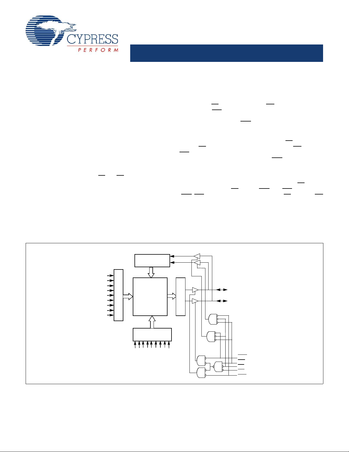
Logic Block Diagram
Note
1. For guidelines on SRAM system design, refer to the “System Design Guidelines” Cypress application note, availa ble at www.cypress.com.
■ Pin and function compatible with CY7C1041CV33
■ High speed
❐ t
= 10 ns
AA
■ Low active power
❐ I
= 90 mA at 10 ns (industrial)
CC
■ Low CMOS standby power
❐ I
= 10 mA
SB2
■ 2.0V data retention
■ Automatic power down when deselected
■ TTL compatible inputs and outputs
■ Easy memory expansion with CE and OE features
■ Available in Pb-free 48-ball VFBGA, 44-pin (400-mil) molded
SOJ, and 44-pin TSOP II packages
Functional Description
The CY7C1041DV33
organized as 256K words by 16 bits. T o write to the device, take
Chip Enable (CE) and Write Enable (WE) inputs LOW. If Byte
LOW Enable (BLE
is written into the location specified on the address pins (A
). If Byte HIGH Enable (BHE) is LOW, then data from IO pins
A
17
(IO
to IO15) is written into the location specified on the address
8
pins (A
to A17).
0
To read from the device, take Chip Enable (CE
Enable (OE
BLE
) LOW while forcing the Write Enable (WE) HIGH. If
is LOW, then data from the memory location specified by
the address pins appears on IO
from memory appears on IO
page 9 for a complete description of read and write modes.
The input and output pins (IO
impedance state when the device is deselected (CE
outputs are disabled (OE
(BHE
, BLE HIGH), or during a write operation (CE LOW and WE
LOW).
The CY7C1041DV33 is available in a standard 44-pin 400-mil
wide SOJ and 44-pin TSOP II package with center power and
ground (revolutionary) pinout and a 48-ball fine-pitch ball g rid
array (FBGA) package.
[1]
is a high performance CMOS Static RAM
) is LOW, then data from IO pins (IO0 to IO7)
to
0
) and Output
to IO7. If BHE is LOW, then data
0
to IO15. See the Truth Table on
8
to IO15) are placed in a high
0
HIGH),
HIGH), BHE and BLE are disabled
Cypress Semiconductor Corporation • 198 Champion Court • San Jose, CA 95134-1709 • 408-943-2600
Document #: 38-05473 Rev. *E Revised July 17, 2008
[+] Feedback [+] Feedback
Page 2
CY7C1041DV33
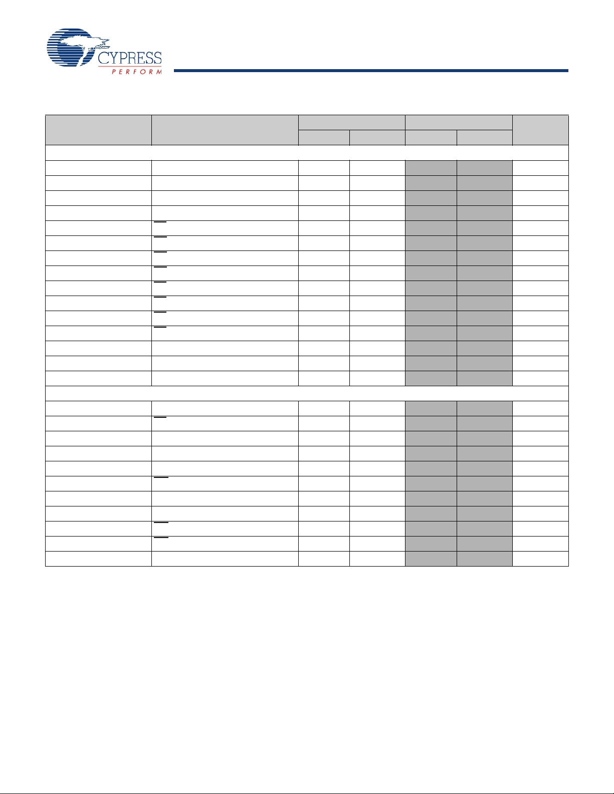
Selection Guide
1
2
3
4
5
6
7
8
9
11
14
31
32
36
35
34
33
37
40
39
38
12
13
41
44
43
42
16
15
29
30
A
17
18
17
20
19
27
28
25
26
22
21
23
24
A
16
A
15
A
0
A
1
A
2
A
3
A
4
A
7
A
6
A
14
A
13
A
12
A
11
A
9
A
8
A
10
OE
BHE
BLE
CE
WE
IO
0
IO
1
IO
2
IO
3
IO
4
IO
5
IO
6
IO
7
IO
8
IO
9
IO
10
IO
11
IO
12
IO
13
IO
14
IO
15
V
CC
V
CC
V
SS
V
SS
NC
10
A
5
WE
V
CC
A
11
A
10
NC
A
6
A
0
A
3
CE
IO
2
IO
0
IO
1
A
4
A
5
IO
3
IO
5
IO
4
IO
6
IO
7
V
SS
A
9
A
8
OE
V
SS
A
7
IO
8
BHE
NC
A
17
A
2
A
1
BLE
V
CC
IO
9
IO
10
IO
11
IO
12
IO
13
IO
14
IO
15
A
15
A
14
A
13
A
12
NC
NC
NC
3
2
6
5
4
1
D
E
B
A
C
F
G
H
A
16
WE
V
CC
A
11
A
10
NC
A
6
A
0
A
3
CE
IO
10
IO
8
IO
9
A
4
A
5
IO
11
IO
13
IO
12
IO
14
IO
15
V
SS
A
9
A
8
OE
V
SS
A
7
IO
0
BHE
NC
A
17
A
2
A
1
BLE
V
CC
IO
2
IO
1
IO
3
IO
4
IO
5
IO
6
IO
7
A
15
A
14
A
13
A
12
NC
NC
NC
3
2
6
5
4
1
D
E
B
A
C
F
G
H
A
16
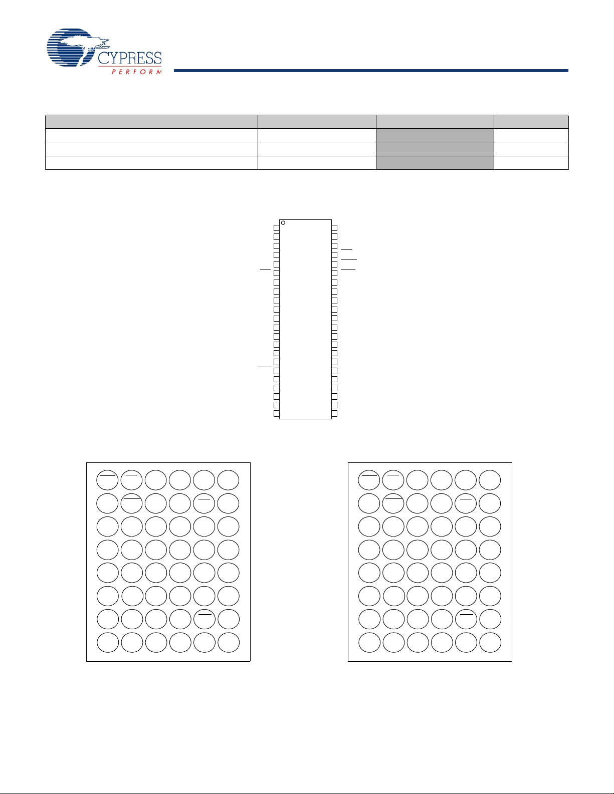
Notes
2. Automotive product information is Preliminary.
3. NC pins are not connected on the die.
4. Pinout 1 is compliant with CY7C1041CV33 and pinout 2 is JE DEC compliant . The diff erence betwe en the two is that the hig her and lower byte IOs (IO
[7:0]
and IO
[15:8]
balls) are swapped.
Description –10 (Industrial) –12 (Automotive)
Maximum Access Time 10 12 ns
Maximum Operating Current 90
95 mA
Maximum CMOS Standby Current 10 15 mA
[2]
Unit
Pin Configuration
Figure 1. 44-Pin SOJ/TSOP II
[3, 4]
Figure 2. 48-Ball VFBGA (Pinout 1)
Document #: 38-05473 Rev. *E Page 2 of 13
Figure 3. 48-Ball VFBGA (Pinout 2)
[3, 4]
[+] Feedback [+] Feedback
Page 3
CY7C1041DV33
Maximum Ratings
Exceeding maximum ratings may shorten the us eful life of the
device. These user guidelines are not tested.
Storage Temperature .................................–65°C to +150°C
Ambient Temperature with
Power Applied ............................................–55°C to +125°C
Supply Voltage on V
DC Voltage Applied to Outputs
in High-Z State
DC Input Voltage
Relative to GND
CC
[5]
.................................. ..–0.3V to VCC +0.3V
[5]
................................–0.3V to VCC +0.3V
[5]
....–0.3V to +4.6V
DC Electrical Characteristics
Over the Operating Range
Parameter Description Test Conditions
V
V
V
V
I
IX
I
OZ
I
CC
I
SB1
I
SB2
OH
OL
IH
IL
[5]
[5]
Output HIGH Voltage VCC = Min, IOH = –4.0 mA 2.4 2.4 V
Output LOW Voltage VCC = Min, IOL = 8.0 mA 0.4 0.4 V
Input HIGH Voltage 2.0 VCC + 0.3 2.0 VCC + 0.3 V
Input LOW Voltage –0.3 0.8 –0.3 0.8 V
Input Leakage Current GND < VI < V
Output Leakage
GND < V
Current
VCC Operating
VCC = Max, f = f
Supply Current
Automatic CE Power Down
Current—TTL Inputs
Automatic CE Power Down
Current—CMOS Inputs
Max VCC, CE > V
VIN > VIH or
< VIL, f = f
V
IN
Max VCC,
CE
> VCC – 0.3V,
V
> VCC – 0.3V,
IN
< 0.3V, f = 0
or V
IN
CC
< VCC, Output Disabled –1 +1 –1 +1 μA
OUT
= 1/tRC100 MHz 90 -mA
MAX
IH
MAX
Current into Outputs (LOW) ........................................20 mA
Static Discharge Voltage............................................>2001V
(MIL-STD-883, Method 3015)
Latch Up Current.....................................................>200 mA
Operating Range
Range
Industrial –40°C to +85°C3.3V ± 0.3V 10 ns
Automotive –40°C to +125°C 3.3V ± 0.3V 12 ns
83 MHz 80
66 MHz 70
40 MHz 60
Ambient
Temperature
V
CC
Speed
–10 (Industrial) –12 (Automotive)
Min Max Min Max
–1 +1 –1 +1 μA
95 mA
85 mA
75 mA
20 25 mA
10
15 mA
Unit
Note
5. Minimum voltage is –2.0V and V
(max) = VCC + 2V for pulse durations of less than 20 ns.
IH
Document #: 38-05473 Rev. *E Page 3 of 13
[+] Feedback [+] Feedback
Page 4
CY7C1041DV33
Capacitance
90%
10%
3.0V
GND
90%
10%
ALL INPUT PULSES
* CAPACITIVE LOAD CONSISTS
OF ALL COMPONENTS OF THE
TEST ENVIRONMENT
Rise Time: 1 V/ns
Fall Time: 1 V/ns
30 pF*
OUTPUT
Z = 50Ω
50Ω
1.5V
(b)
(a)
3.3V
OUTPUT
5 pF
(c)
R 317Ω
R2
351Ω
High-Z Characteristics
10 ns device
Notes
6. Tested initially and after any design or process changes that may affect these parameters.
7. AC characteristics (except High-Z) are tested using the load conditions shown in AC Test Loads and Waveforms (a). High-Z characteristics are tested for all speeds
using the test load shown in (c).
[6]
Parameter Description Test Conditions Max Unit
C
C
IN
OUT
Input Capacitance TA = 25°C, f = 1 MHz, VCC = 3.3V 8 pF
IO Capacitance 8 pF
Thermal Resistance
[6]
Parameter Description Test Condit ion s
Θ
Θ
Thermal Resistance (Junction
JA
to Ambient)
Thermal Resistance (Junction
JC
to Case)
Still Air, soldered on a 3 × 4.5 inch,
four layer printed circuit board
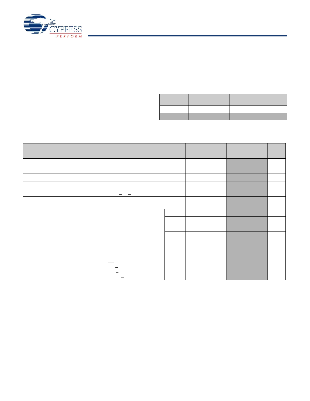
AC Test Loads and Waveforms
The AC test loads and waveform diagram follows.
[7]
FBGA
Package
SOJ
Package
TSOP II
Package
27.89 57.91 50.66 °C/W
14.74 36.73 17.17 °C/W
Unit
Document #: 38-05473 Rev. *E Page 4 of 13
[+] Feedback [+] Feedback
Page 5
CY7C1041DV33
AC Switching Characteristics Over the Operating Range
Notes
8. Test conditions assume signal transition time of 3 ns or less, timing reference levels of 1.5V, input pulse levels of 0 to 3.0V, and output loading of the specified I
OL/IOH
and 30-pF load capacitance.
9. t
POWER
gives the minimum amount of time that the power supply should be at typical VCC values until the first memory access is performed.
10.t
HZOE
, t
HZCE
, t
HZBE,
and t
HZWE
are specified with a load capacitance of 5 pF as in part (c) of AC Test Loads and Waveforms. Transition is measured when the outp uts enter
a high impedance state.
11.At any given temperature and voltage condition, t
HZCE
is less than t
LZCE
, t
HZOE
is less than t
LZOE
, t
HZBE
is less than t
LZBE
, and t
HZWE
is less than t
LZWE
for any given
device.
[8]
Parameter Description
Read Cycle
[9]
t
power
t
RC
t
AA
t
OHA
t
ACE
t
DOE
t
LZOE
t
HZOE
t
LZCE
t
HZCE
t
PU
t
PD
t
DBE
t
LZBE
t
HZBE
Write Cycle
t
WC
t
SCE
t
AW
t
HA
t
SA
t
PWE
t
SD
t
HD
t
LZWE
t
HZWE
t
BW
[12, 13]
VCC(Typical) to the First Access 100 100 μs
Read Cycle Time 10 12 ns
Address to Data Valid 10 12 ns
Data Hold from Address Change 3 3 ns
CE LOW to Data Valid 10 12 ns
OE LOW to Data Valid 5 6ns
OE LOW to Low-Z 0 0 ns
OE HIGH to High-Z
CE LOW to Low-Z
CE HIGH to High-Z
CE LOW to Power Up 0 0 ns
CE HIGH to Power Down 10 12 ns
Byte Enable to Data Valid 5 6ns
Byte Enable to Low-Z 0 0 ns
Byte Disable to High-Z 6 6ns
Write Cycle Time 10 12 ns
CE LOW to Write End 7 8 ns
Address Setup to Write End 7 8 ns
Address Hold from Write End 0 0 ns
Address Setup to Write Start 0 0 ns
WE Pulse Width 7 8 ns
Data Setup to Write End 5 6 ns
Data Hold from Write End 0 0 ns
WE HIGH to Low-Z
WE LOW to High-Z
Byte Enable to End of Write 7 8 ns
[10, 11]
[11]
[10, 11]
[11]
[10, 11]
–10 (Industrial) –12 (Automotive)
Min Max Min Max
5 6ns
3 3 ns
5 6ns
3 3 ns
5 6ns
Unit
Document #: 38-05473 Rev. *E Page 5 of 13
[+] Feedback [+] Feedback
Page 6

CY7C1041DV33
Data Retention Characteristics Over the Operating Range
3.0V3.0V
t
CDR
VDR> 2V
DATA RETENTION MODE
t
R
CE
V
CC
PREVIOUS DATA VALID DATA VALID
t
RC
t
AA
t
OHA
ADDRESS
DATA OUT
Notes
12.The internal write time of the memory is defined by the overlap of CE
LOW and WE LOW. CE and WE must be LOW to initiate a write and the transition of either of
these signals can terminate the write. The input data setup and hold timing should be referenced to the leading edge of the signal that terminates the write.
13.The minimum write cycle time for Write Cycle No. 4 (WE
controlled, OE LOW) is the sum of t
HZWE
and tSD.
14.No input may exceed V
CC
+ 0.3V.
15.Full device operation requires linear V
CC
ramp from V
DR
to V
CC(min.)
> 50 μs or stable at V
CC(min.)
> 50 μs.
16.Device is continuously selected. OE
, CE, BHE, and BHE = VIL.
17.WE
is HIGH for read cycle.
Parameter Description Conditions
V
DR
I
CCDR
t
CDR
[15]
t
R
[6]
VCC for Data Retention 2.0 V
Data Retention Current VCC = VDR = 2.0V,
CE
> VCC – 0.3V,
> VCC – 0.3V or VIN < 0.3V
V
IN
Chip Deselect to Data Retention Time 0 ns
Operation Recovery Time t
Data Retention Waveform
Switching Waveforms
Figure 4. Read Cycle No. 1
[16, 17]
[14]
Min Max Unit
Ind’l 10 mA
Auto 15
RC
mA
ns
Document #: 38-05473 Rev. *E Page 6 of 13
[+] Feedback [+] Feedback
Page 7

CY7C1041DV33
Switching Waveforms (continued)
50%
50%
DATA VALID
t
RC
t
ACE
t
DOE
t
LZOE
t
LZCE
t
PU
HIGH IMPEDANCE
t
HZOE
t
HZBE
t
PD
HIGH
OE
CE
ICC
ISB
IMPEDANCE
ADDRESS
DATA OUT
V
CC
SUPPLY
t
DBE
t
LZBE
t
HZCE
BHE, BLE
CURRENT
I
CC
I
SB
t
HD
t
SD
t
SCE
t
SA
t
HA
t
AW
t
PWE
t
WC
BW
DATAIO
ADDRESS
CE
WE
BHE, BLE
t
Notes
18.Address valid prior to or coincident with CE
transition LOW.
19.Data IO is high impedance if OE
or BHE and BLE = V
IH.
20.If CE goes HIGH simultaneously with WE going HIGH, the output remains in a high impedance state.
Figure 5. Read Cycle No. 2 (OE Controlled)
[17, 18]
Figure 6. Write Cycle No. 1 (CE Controlled)
Document #: 38-05473 Rev. *E Page 7 of 13
[19, 20]
[+] Feedback [+] Feedback
Page 8

CY7C1041DV33
Switching Waveforms (continued)
t
HD
t
SD
t
BW
t
SA
t
HA
t
AW
t
PWE
t
WC
t
SCE
DATAIO
ADDRESS
BHE
,BLE
WE
CE
t
HD
t
SD
t
PWE
t
SA
t
HA
t
AW
t
SCE
t
WC
t
HZOE
DATAIN VALID
CE
ADDRESS
WE
DATA IO
OE
NOTE 21
BHE,BLE
Note
21.During this period the IOs are in the output state and input signals should not be applied.
Figure 7. Write Cycle No. 2 (BLE or BHE Controlled)
Figure 8. Write Cycle No. 3 (WE Controlled, OE HIGH During Write)
[19, 20]
Document #: 38-05473 Rev. *E Page 8 of 13
[+] Feedback [+] Feedback
Page 9

CY7C1041DV33
Switching Waveforms (continued)
t
HD
t
SD
t
SCE
t
HA
t
AW
t
PWE
t
WC
t
BW
DATA IO
ADDRESS
CE
WE
BHE
,BLE
t
SA
t
LZWE
t
HZWE
NOTE 21
Figure 9. Write Cycle No. 4 (WE Controlled, OE LOW)
T ruth Table
CE OE WE BLE BHE
IO0–IO
7
IO8–IO
15
Mode Power
H X X X X High-Z High-Z Power Down Standby (I
L L H L L Data Out Data Out Read All Bits Active (I
L L H L H Data Out High-Z Read Lower Bits Only Active (I
L L H H L High-Z Data Out Read Upper Bits Only Active (I
L X L L L Data In Data In Write All Bits Active (I
L X L L H Data In High-Z Write Lower Bits Only Active (I
L X L H L High-Z Data In Write Upper Bits Only Active (I
L H H X X High-Z High-Z Selected, Outputs Disabled Active (I
CC
CC
CC
CC
CC
CC
CC
SB
)
)
)
)
)
)
)
)
Document #: 38-05473 Rev. *E Page 9 of 13
[+] Feedback [+] Feedback
Page 10

CY7C1041DV33
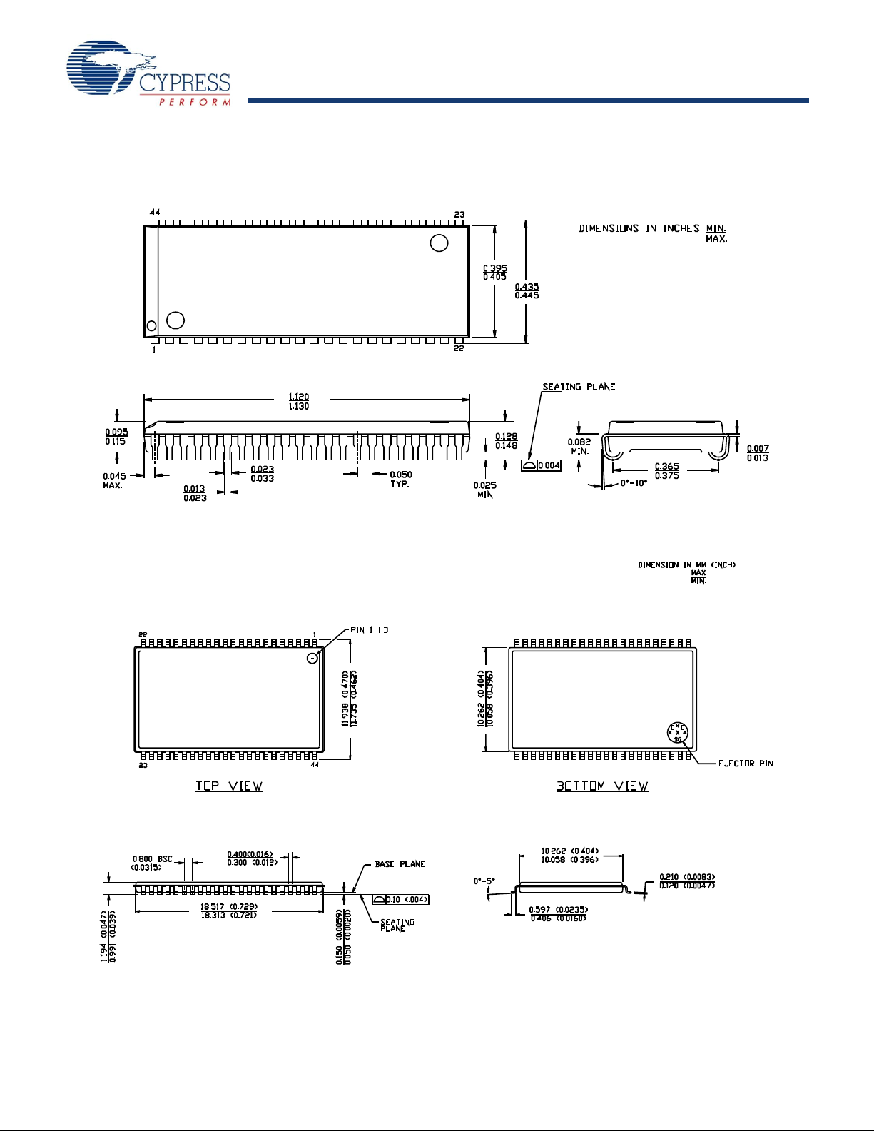
Ordering Information
A
1
A1 CORNER
0.75
0.75
Ø0.30±0.05(48X)
Ø0.25 M C A B
Ø0.05 M C
B
A
0.15(4X)
0.21±0.05
1.00 MAX
C
SEATING PLANE
0.55 MAX.
0.25 C
0.10 C
A1 CORNER
TOP VIEW
BOTTOM VIEW
234
3.75
5.25
B
C
D
E
F
G
H
65
465231
D
H
F
G
E
C
B
A
6.00±0.10
8.00±0.10
A
8.00±0.10
6.00±0.10
B
1.875
2.625
0.26 MAX.
51-85150-*D
Speed
(ns) Ordering Code
10 CY7C1041DV33-10BVI 51-85150 48-Ball VFBGA Industrial
CY7C1041DV33-10BVXI 48-Ball VFBGA (Pb-Free) Pinout - 1
CY7C1041DV33-10BVJXI 48-Ball VFBGA (Pb-Free) Pinout - 2
CY7C1041DV33-10VXI 51-85082 44-Pin (400-mil) Molded SOJ (Pb-Free)
CY7C1041DV33-10ZSXI 51-85087 44-Pin TSOP II (Pb-Free)
12 CY7C1041DV33-12BVXE 51-85150 48-Ball VFBGA (Pb-Free) Automotive
CY7C1041DV33-12VXE 51-85082 44-Pin (400-mil) Molded SOJ (Pb-Free)
CY7C1041DV33-12ZSXE 51-85087 44-Pin TSOP II (Pb-Free)
Please contact your local Cypress sales representative for availability of these parts
Package
Diagram Package Type
[4]
[4]
Package Diagrams
Figure 10. 48-Ball VFBGA (6 x 8 x 1 mm) (51-85150)
Operating
Range
a
Document #: 38-05473 Rev. *E Page 10 of 13
[+] Feedback [+] Feedback
Page 11
CY7C1041DV33
Package Diagrams(continued)
51-85082-*B
51-85087-*A
Figure 11. 44-Pin (400-mil) Molded SOJ (51-85082)
Figure 12. 44-Pin TSOP II (51-85087)
Document #: 38-05473 Rev. *E Page 1 1 of 13
[+] Feedback [+] Feedback
Page 12

CY7C1041DV33
Document History Page
Document Title: CY7C1041DV33 4 Mbit (256K x 16) Static RAM
Document Number: 38-05473
Rev. ECN No.
Orig. of
Change
** 201560 SWI See ECN Advance Data sheet for C9 IPP
*A 233729 RKF See ECN 1.AC, DC parameters are modified as per EROS(Spec # 01-2165)
*B 351117 PCI See ECN Changed from Advance to Preliminary
*C 446328 NXR See ECN Converted from Prelimi nary to Final
*D 480177 VKN See ECN Added -10BVI product ordering code in the Ordering Information table
*E 2541850 VKN/PYRS 07/22/08 Added -10BVJXI part
Submission
Date
Description of Change
2.Pb-free offering in the ‘Ordering information’
Removed 15 and 20 ns Speed bin
Corrected DC voltage (min) value in maximum ratings section from - 0.5 to
- 0.3V
Redefined I
(Com’l): Changed from 100, 80 and 67 mA to 90, 80 and 75 mA for 8, 10
I
CC
and 12ns speed bins respectively
I
(Ind’l): Changed from 80 and 67 mA to 90 and 85 mA for 10 and 12ns speed
CC
bins respectively
values for Com’l and Ind’l temperature ranges
CC
Added Static Discharge Voltage and latch-up current spec
Added V
Changed Note# 4 on AC Test Loads
) spec in Note# 2
IH(max
Changed reference voltage level for measurement of Hi-Z parameters from
±500 mV to ±200 mV
Added Data Retention Characteristics/Waveform and footnote # 11, 12
Added Write Cycle (WE
Controlled, OE HIGH During Write) Timing Diagram
Changed Package Diagram name from 44-Pin TSOP II Z44 to 44-Pin TSOP II
ZS44 and from 44-Pin (400-mil) Molded SOJ V34 to 44-Pin (400-mil) Molded
SOJ V44
Changed part names from Z to ZS in the Ordering Information Tabl e
Added 8 ns Product Information
Added Pin-Free Ordering Information
Shaded Ordering Information Table
Removed -8 speed bin
Removed Commercial Operating Range product information
Included Automotive Operating Range product information
Updated Thermal Resistance table
Updated footnote #8 on High-Z parameter measurement
Updated the ordering information and replaced Package Name column with
Package Diagram in the Ordering Information Table
Document #: 38-05473 Rev. *E Page 12 of 13
[+] Feedback [+] Feedback
Page 13

CY7C1041DV33
Sales, Solutions, and Legal Information
Worldwide Sales and Design Support
Cypress maintains a worldwide network of offices, solution centers, manufacturer’s representatives, and distributors. T o find the office
closest to you, visit us at cypress.com/sales.
Products
PSoC psoc.cypress.com
Clocks & Buffers clocks.cypress.com
Wireless wireless.cypress.com
Memories memory.cypress.com
Image Sensors image.cypress.com
PSoC Solutions
General psoc.cypress.com/solutions
Low Power/Low Voltage psoc.cypress.com/low-power
Precision Analog psoc.cypress.com/precision-analog
LCD Drive psoc.cypress.com/lcd-drive
CAN 2.0b psoc.cypress.com/can
USB psoc.cypress.com/usb
© Cypress Semiconductor Corporation, 2004-2008. The information contained herein is subject to change without notice. Cypress Semiconductor Corporation assumes no responsibility for the use
of any circuitry other than circuitry embodied in a Cypress product. Nor does it convey or imply any license under patent or other rights. Cypress products are not warranted nor intended to be used
for medical, life support, life sa vin g, critical control or safety applicati ons, un l ess p ur sua nt to an express written agreement wi th Cy press. Furthermore, Cypress does not authorize its products for use
as critical components in life-support systems where a malfunction or failure may reasonably be expected to result in significant injury to the user. The inclusion of Cypress products in life-support
systems application implies that the manufacturer assumes all risk of such use and in doing so indemnifies Cypress against all charges.
Any Source Code (software and/or firmware) is owned by Cypress Semiconductor Corporation (Cypress) and is protected by and subject to worldwide patent protection (United States and foreign),
United States co pyright la ws and inte rnatio na l tre aty prov isi ons. Cyp ress he reby g rant s to lice nsee a p erson al, no n-ex clusi ve, non-tra nsferable license to copy, use, modify, create derivative works of,
and compile the Cypress Source Code and derivative works for the sole purpo se of creating custom sof tware and or firm ware in support of licen see product to be use d only in conjunction with a Cypress
integrated circuit as specified in th e applicable agreement. Any reproductio n, modification, translation, co mpilation, o r representati on of this Sour ce Code except as specified above is prohibited without
the express written permission of Cypress.
Disclaimer: CYPRESS MAKES NO WARRANTY OF ANY KIND, EXPRESS OR IMPLIED, WITH REGARD TO THIS MATERIAL, INCLUDING, BUT NOT LIMITED TO, THE IMPLIED WARRANTIES
OF MERCHANTABILITY AND FITNESS FOR A PARTICULAR PURPOSE. Cypress reserves the right to make changes without further notice to the materials described herein. Cypress does not
assume any liability arising out of the ap plicati on or u se o f any pr oduct o r circui t descri bed h erein. Cypr ess does not aut horize it s product s for use a s critical compo nent s in life-support systems whe re
a malfunction or failure may reasonab ly be expected to resu lt in significant injury t o the user. The inclusion of Cypress’ prod uct in a life-support systems application implies that the manufacturer
assumes all risk of such use and in doing so indemnifies Cypress against all charges.
Use may be limited by and subject to the applicable Cypress software license agreement.
Document #: 38-05473 Rev. *E Revised July 17, 2008 Page 13 of 13
All product and company names mentioned in this document are the trademarks of their respective holders.
[+] Feedback [+] Feedback
 Loading...