

Page 1
CY7C1012DV33
12-Mbit (512K X 24) Static RAM
Features
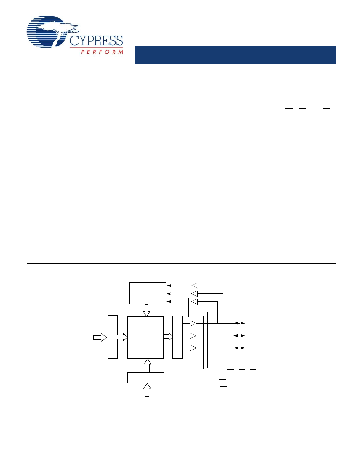
Logic Block Diagram
COLUMN
DECODER
ROW DECODER
SENSE AMPS
INPUT BUFFER
512K x 24
ARRAY
I/O0 – I/O
7
OE
I/O8 – I/O
15
CE1, CE2, CE
3
WE
I/O
16
– I/O
23
CONTROL LOGIC
A
(9:0)
A
(18:10)
■
High speed
❐
tAA = 10 ns
■
Low active power
❐
ICC = 175 mA at 10 ns
■
Low CMOS standby power
❐
I
= 25 mA
SB2
■
Operating voltages of 3.3 ± 0.3V
■
2.0V data retention
■
Automatic power down when deselected
■
TTL compatible inputs and outputs
■
Available in Pb-free standard 119-ball PBGA
Functional Description
The CY7C1012DV33 is a high performance CMOS static RAM
organized as 512K words by 24 bits. Each data byte is separately
controlled by the individual chip selects (CE1, CE2, and CE3).
CE
controls the data on the I/O0 – I/O7, while CE2 controls the
1
data on I/O
I/O
16
that significantly reduces power consumption when deselected.
Writing the data bytes into the SRAM is accomplished when the
chip select controlling that byte is LOW and the write enable input
(WE
) input is LOW. Data on the respective input and output (I/O)
pins is then written into the location specified on the address pins
(A0 – A18). Asserting all of the chip selects LOW and write enable
LOW writes all 24 bits of data into the SRAM. Output enable (OE
is ignored while in WRITE mode.
Data bytes are also individually read from the device. Reading a
byte is accomplished when the chip select cont rolling that byte
is LOW and write enable (WE
remains LOW. Under these conditions, the contents of the
memory location specified on the address pins appear on the
specified data input and output (I/O) pins. Asserting all the chip
selects LOW reads all 24 bits of data from the SRAM.
The 24 I/O pins (I/O
state when all the chip selects are HIGH or when the output
enable (OE) is HIGH during a READ mode. For more information, see the Truth Table on page 8.
– I/O15, and CE3 controls the data on the data pins
8
– I/O23. This device has an automatic power down feature
) HIGH, while output enable (OE)
– I/O23) are placed in a high impedance
0
)
Cypress Semiconductor Corporation • 198 Champion Court • San Jose,CA 95134-1709 • 408-943-2600
Document Number: 38-05610 Rev. *D Revised November 6, 2008
[+] Feedback
Page 2
CY7C1012DV33
Selection Guide
1 2 3 4 5 6 7
A NCAAAAANC
B NC A A CE
1
AANC
C I/O
12
NC CE
2
NC CE
3
NC I/O
0
D I/O
13
V
DD
V
SS
V
SS
V
SS
V
DD
I/O
1
E I/O
14
V
SS
V
DD
V
SS
V
DD
V
SS
I/O
2
F I/O
15
V
DD
V
SS
V
SS
V
SS
V
DD
I/O
3
G I/O
16
V
SS
V
DD
V
SS
V
DD
V
SS
I/O
4
H I/O
17
V
DD
V
SS
V
SS
V
SS
V
DD
I/O
5
J NC V
SS
V
DD
V
SS
V
DD
V
SS
NC
K I/O
18
V
DD
V
SS
V
SS
V
SS
V
DD
I/O
6
L I/O
19
V
SS
V
DD
V
SS
V
DD
V
SS
I/O
7
M I/O
20
V
DD
V
SS
V
SS
V
SS
V
DD
I/O
8
N I/O
21
V
SS
V
DD
V
SS
V
DD
V
SS
I/O
9
P I/O
22
V
DD
V
SS
V
SS
V
SS
V
DD
I/O
10
R I/O
23
A NCNCNC AI/O
11
T NC A A WE AANC
U NC A A OE AANC
Note
1. NC pins are not connected on the die.
Description –10 Unit
Maximum Access Time 10 ns
Maximum Operating Current 175 mA
Maximum CMOS Standby Current 25 mA
Pin Configuration
Figure 1. 119-Ball PBGA (
Top View)
[1]
Document Number: 38-05610 Rev. *D Page 2 of 11
[+] Feedback
Page 3
CY7C1012DV33
Maximum Ratings
Notes
2. V
IL
(min) = –2.0V and VIH(max) = VCC + 2V for pulse durations of less than 20 ns.
3. CE
indicates a combination of all three chip enables. When active LOW, CE indicates the CE1 or CE
2 ,
or CE3 is LOW. When HIGH, CE indicates the CE
1 , CE2 ,
and
CE
3
are HIGH.
Exceeding maximum ratings may impair the useful life of the
device. These user guidelines are not tested.
Storage Temperature .................................–65°C to +150°C
Ambient Temperature with
Power Applied ............................................–55°C to +125°C
Supply Voltage on V
DC Voltage Applied to Outputs
in High-Z State
DC Input Voltage
Relative to GND
CC
[2]
..................................–0.5V to VCC + 0.5V
[2]
...............................–0.5V to VCC + 0.5V
[2]
....–0.5V to +4.6V
Current into Outputs (LOW) ..................... ... ................20 mA
Static Discharge Voltage............................................>2001V
(MIL-STD-883, Method 3015)
Latch Up Current.....................................................>200 mA
Operating Range
Range
Industrial –40°C to +85°C3.3V ± 0.3V
Ambient
T emperature
V
CC
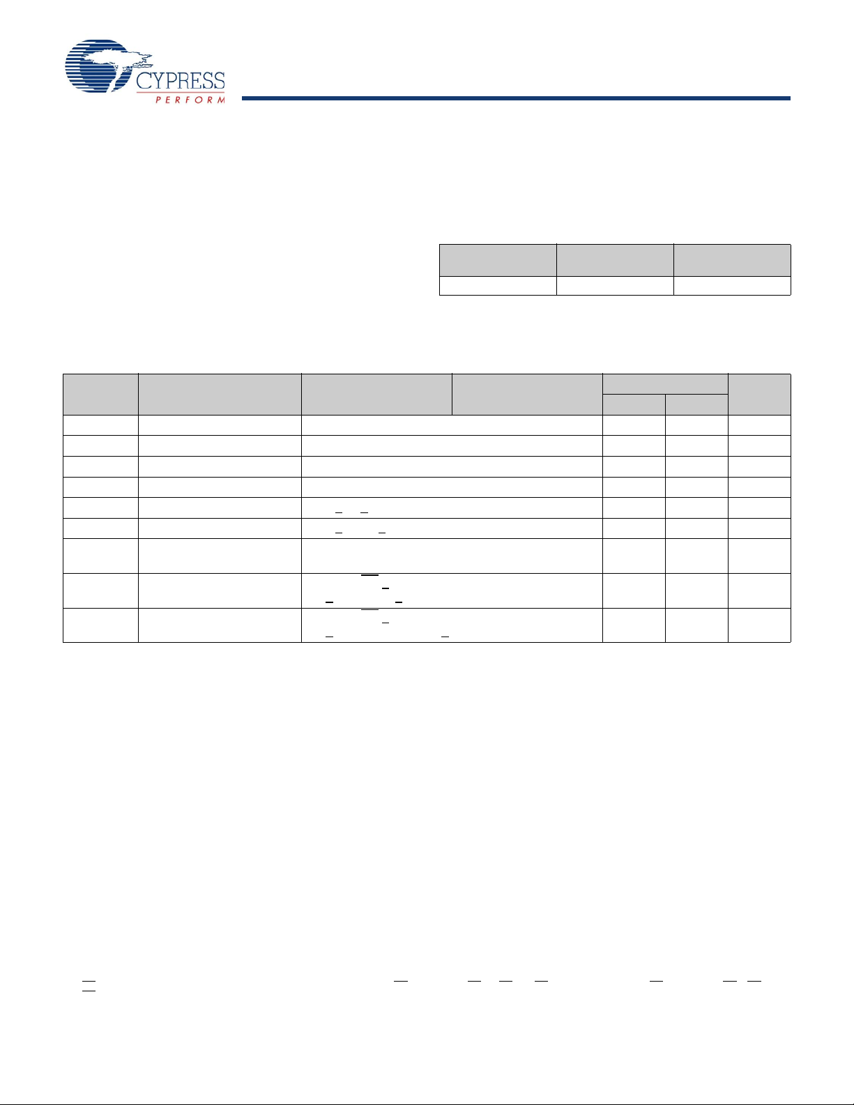
DC Electrical Characteristics
Over the Operating Range
Parameter Description Test Conditions
V
V
V
V
I
I
I
I
I
OH
OL
IH
IL
IX
OZ
CC
SB1
SB2
[2]
Output HIGH Voltage VCC = Min, IOH = –4.0 mA 2.4 V
Output LOW Voltage VCC = Min, IOL = 8.0 mA 0.4 V
Input HIGH Voltage 2.0 VCC + 0.3 V
Input LOW Voltage –0.3 0.8 V
Input Leakage Current GND < VI < V
Output Leakage Current GND < V
VCC Operating Supply
Current
Automatic CE Power Down
Current —TTL Inputs
Automatic CE Power Down
Current —CMOS Inputs
VCC = Max, f = f
I
= 0 mA CMOS levels
OUT
Max VCC, CE > V
VIN > VIH or VIN < VIL, f = f
Max VCC, CE > VCC – 0.3V,
V
> VCC – 0.3V, or VIN < 0.3V, f = 0
IN
CC
< VCC, output disabled –1 +1 μA
OUT
MAX
IH
[3]
= 1/t
RC
MAX
–10
Min Max
Unit
–1 +1 μA
175 mA
30 mA
25 mA
Document Number: 38-05610 Rev. *D Page 3 of 11
[+] Feedback
Page 4
CY7C1012DV33
Capacitance
90%
10%
3.0V
GND
90%
10%
All input pulses
3.3V
OUTPUT
5 pF*
(a)
(b)
R1 317 Ω
R2
351Ω
Fall Time:> 1V/ns
(c)
OUTPUT
50Ω
Z0= 50Ω
V
TH
= 1.5V
30 pF*
*
Capacitive Load consists of all
components of the test environment
Rise Time > 1V/ns
*Including jig
and scope
Note
4. Valid SRAM operation does not occur u ntil t he power sup plies ha ve rea ched t he minimum o peratin g V
DD
(3.0V). 100μs (t
power
) after reaching the minimum operating
V
DD
, normal SRAM operation begins including reduction in VDD to the data retention (V
CCDR
, 2.0V) voltage.
Tested initially and after any design or process chang es that may affect these parameters
.
Parameter Description Test Conditions Max Unit
C
C
IN
OUT
Input Capacitance TA = 25°C, f = 1 MHz, VCC = 3.3V 8 pF
I/O Capacitance 10 pF
Thermal Resistance
Tested initially and after any design or process changes that may affect these parameters.
Parameter Description Test Conditions
Θ
Θ
Thermal Resistance
JA
(junction to ambient)
Thermal Resistance
JC
(junction to case)
Still air, soldered on a 3 × 4.5 inch,
four layer printed circuit board
Figure 2. AC Test Loads and Waveforms
[4]
119-Ball
PBGA
20.31 °C/W
8.35 °C/W
Unit
Document Number: 38-05610 Rev. *D Page 4 of 11
[+] Feedback
Page 5

CY7C1012DV33
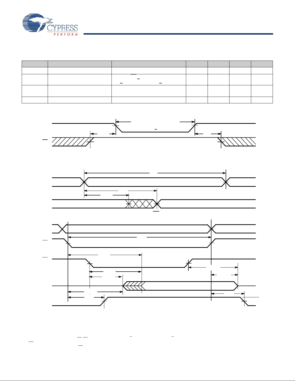
AC Switching Characteristics
Notes
5. T est condi tio ns assume signal transi tio n time of 3 ns or less , timing refe rence levels of 1.5V, and input pulse levels of 0 to 3.0V . Test conditions for the read cycle use
output loading as shown in part a) of Figure 2, unless specified otherw is e .
6. t
POWER
gives the minimum amount of time that the power supply is at typical VCC values until the first memory access is performed.
7. t
HZOE
, t
HZCE
, t
HZWE
, t
LZOE
, t
LZCE
, and t
LZWE
are specified with a load capacitance of 5 pF as in part (b) of Figure2. Transition is measured ±200 mV from steady stat e
voltage.
8. These parameters are guaranteed by design and are not tested.
9. The internal write time of the memory is defined by the overlap of CE
1
or CE2 or CE3 LOW and WE LOW. Chip enables must be active and WE must be LOW to initia te
a write. The transition of any of these signals termina te the wr ite. The input dat a se tup an d hold timing a re refe renced to t he lead ing edge of the signal t hat termin ates
the write.
10.The minimum write cycle time for Write Cycle No. 3 (WE
controlled, OE LOW) is the sum of t
HZWE
and tSD.
Over the Operating Range
Parameter Description
Read Cycle
[6]
t
power
t
RC
t
AA
t
OHA
t
ACE
t
DOE
t
LZOE
t
HZOE
t
LZCE
t
HZCE
t
PU
t
PD
Write Cycle
t
WC
t
SCE
t
AW
t
HA
t
SA
t
PWE
t
SD
t
HD
t
LZWE
t
HZWE
[9, 10]
[5]
VCC(Typical) to the First Access 100 μs
Read Cycle Time 10 ns
Address to Data Valid 10 ns
Data Hold from Address Change 3 ns
CE Active LOW to Data Va lid
OE LOW to Data Valid 5 ns
OE LOW to Low Z
OE HIGH to High Z
[7]
[7]
CE Active LOW to Low Z
CE Deselect HIGH to High Z
CE Active LOW to Power Up
CE Deselect HIGH to Power Down
Write Cycle Time 10 ns
CE Active LOW to Write End
Address Setup to Write End 7 ns
Address Hold from Write End 0 ns
Address Setup to Write Start 0 ns
WE Pulse Width 7 ns
Data Setup to Write End 5.5 ns
Data Hold from Write End 0 ns
WE HIGH to Low Z
WE LOW to High Z
[7]
[7]
[3, 7]
[3]
[3, 7]
[3, 8]
[3]
[3, 8]
–10
Min Max
Unit
10 ns
1ns
5ns
3ns
5ns
0ns
10 ns
7ns
3ns
5ns
Document Number: 38-05610 Rev. *D Page 5 of 11
[+] Feedback
Page 6
CY7C1012DV33
Data Retention Characteristics
3.0V3.0V
t
CDR
V
DR
>
2V
DATA RETENTION MODE
t
R
CE
V
CC
PREVIOUS DATA VALID DATA VALID
RC
t
AA
t
OHA
t
RC
ADDRESS
DATA OUT
50%
50%
DATA VALID
t
RC
t
ACE
t
DOE
t
LZOE
t
LZCE
t
PU
HIGH IMPEDANCE
t
HZOE
t
PD
t
HZCE
OE
CE
ADDRESS
DATA OUT
V
CC
SUPPLY
CURRENT
HIGH
IMPEDANCE
I
CC
I
SB
Notes
11.Tested initially and after any design or process changes that may affect these parameters.
12.Full device operation requires linear V
CC
ramp from V
DR
to V
CC(min)
> 50 μs or stable at V
CC(min)
> 50 μs.
13.Device is continuously selected. OE
, CE = VIL.
14.WE
is HIGH for read cycle.
15.Address valid before or similar to CE
transition LOW.
Over the Operating Range
Parameter Description Conditions
V
DR
I
CCDR
t
CDR
t
R
[11]
[12]
VCC for Data Retention 2 V
Data Retention Current V
= 2V , CE > VCC – 0.2V,
CC
VIN > VCC – 0.2V or VIN < 0.2V
Chip Deselect to Data Retention
Time
Operation Recovery Time t
Data Retention Waveform
Switching Waveforms
Figure 3. Read Cycle No. 1
[3]
[13, 14]
Min Typ Max Unit
25 mA
0ns
RC
ns
Figure 4. Read Cycle No. 2 (OE Controlled)
Document Number: 38-05610 Rev. *D Page 6 of 11
[3, 14, 15]
[+] Feedback
Page 7

CY7C1012DV33
Switching Waveforms
t
WC
DATA VALID
t
AW
t
SA
t
PWE
t
HA
t
HD
t
SD
t
SCE
t
SCE
CE
WE
DATA I/O
ADDRESS
t
HD
t
SD
t
PWE
t
SA
t
HA
t
AW
t
SCE
t
WC
t
HZOE
DATAINVALID
CE
ADDRESS
WE
DATA I/O
OE
NOTE 18
DATA VALID
t
HD
t
SD
t
LZWE
t
PWE
t
SA
t
HA
t
AW
t
SCE
t
WC
t
HZWE
CE
ADDRESS
WE
DATA I/O
NOTE
18
Notes
16.Data I/O is high impedance if OE
= VIH.
17.If CE
goes HIGH simultaneously with WE going HIGH, the output remains in a high impedance state.
18.During this period, the I/Os are in output state. Do not apply input signals.
(continued)
Figure 5. Write Cycle No. 1 (CE
Controlled)
[3, 16, 17]
Figure 6. Write Cycle No. 2 (W E Controlled, OE HIGH During Write)
Figure 7. Write Cycle No. 3 (WE Controlled, OE LOW)
[3, 17]
[3, 16, 17]
Document Number: 38-05610 Rev. *D Page 7 of 11
[+] Feedback
Page 8

CY7C1012DV33
T ruth Table
CE
H H H X X High Z High Z High Z Power Down Standby (I
H L H L H High Z Data Out High Z Read Active (I
H H L L H High Z High Z Data Out Read Active (I
H L H X L High Z Data In High Z Write Active (I
H H L X L High Z High Z Data In Write Active (I
CE
1
L H H L H Data Out High Z High Z Read Active (I
LLLLHFull Data OutFull Data OutFull Data OutRead Active (I
L H H X L Data In High Z High Z Write Active (I
L L L X L Full Data In Full Data In Full Data In Write Active (I
L L L H H High Z High Z High Z Selected,
CE
2
OE WE I/O0 – I/O7 I/O8 – I/O15 I/O
3
– I/O23 Mode Power
16
Active (I
Outputs Disabled
CC
CC
CC
CC
CC
CC
CC
CC
CC
SB
)
)
)
)
)
)
)
)
)
)
Document Number: 38-05610 Rev. *D Page 8 of 11
[+] Feedback
Page 9
CY7C1012DV33
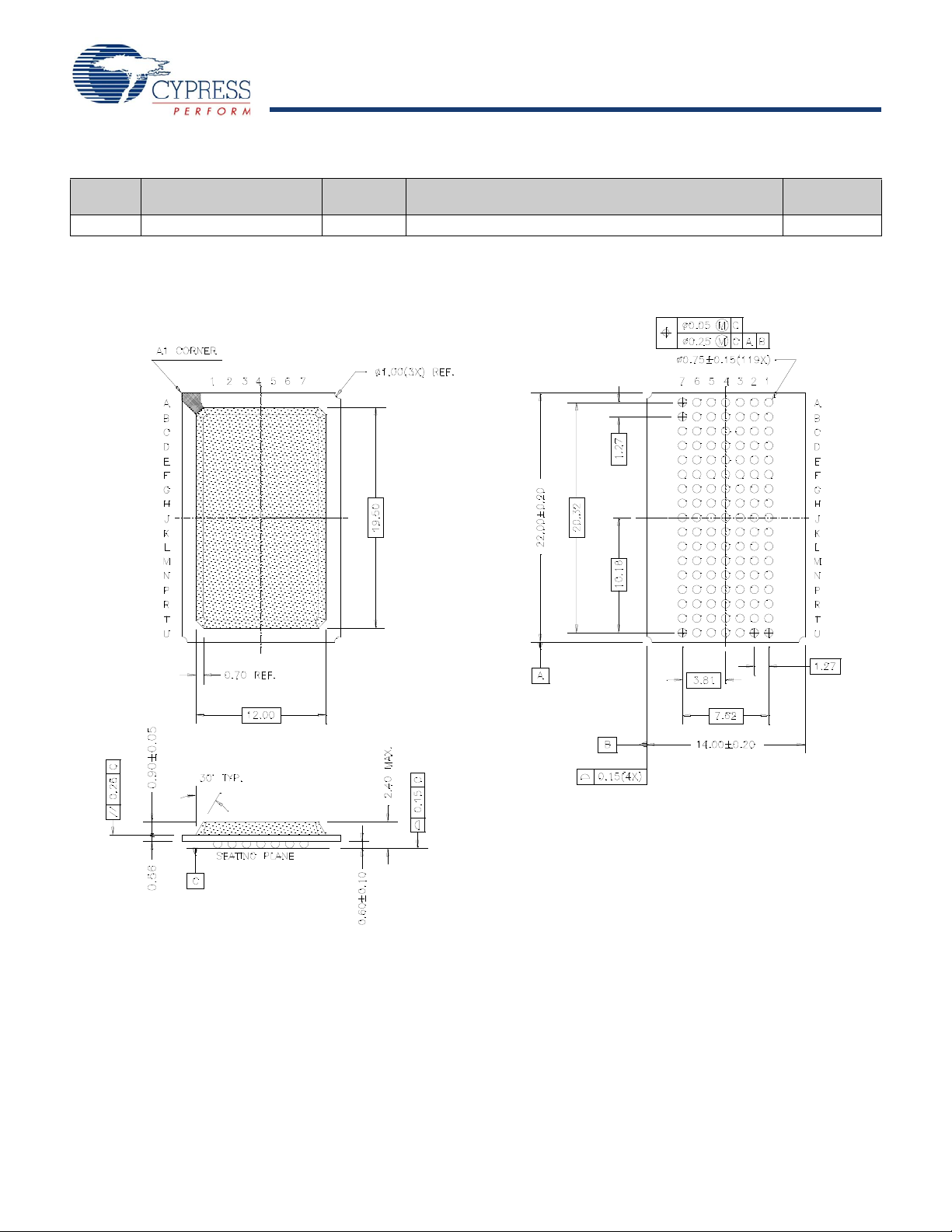
Ordering Information
51-85115-*B
Speed
(ns)
10 CY7C1012DV33-10BGXI 51-85115 1 19-Ball Plastic Ball Grid Array (14 x 22 x 2.4 mm) (Pb-Free) Industrial
Ordering Code
Package
Name
Package Type
Package Diagram
Figure 8. 119-Ball PBGA (14 x 22 x 2.4 mm)
Operating
Range
Document Number: 38-05610 Rev. *D Page 9 of 11
[+] Feedback
Page 10

CY7C1012DV33
Document History Page
Document Title: CY7C1012DV33 12-Mbit (512K X 24) Static RAM
Document Number: 38-05610
Rev. ECN No.
Orig. of
Change
** 250650 SYT See ECN New data sheet
*A 469517 NXR See ECN Converted from Advance Information to Preliminary
*B 499604 NXR See ECN Added note 1 for NC pins
*C 1462585 VKN See ECN Converted from preliminary to final
*D 2604677 VKN/PYRS 11/12/08 Removed Commercial operating range, Added Industrial operating range
Submission
Date
Description of Change
Corrected typo in the Document Title
Removed –10 and –12 speed bins from product offering
Changed J7 Ball of BGA from DNU to NC
Removed Industrial Operating range from product offering
Included the Maximum ratings for Static Discharge Voltage and Latch Up Current
on page 3
Changed I
Changed I
Changed I
Specified the Overshoot specification in footnote 1
from 220 mA to 150 mA
CC(Max)
SB1(Max)
SB2(Max)
from 70 mA to 30 mA
from 40 mA to 25 mA
Updated the Truth Table
Updated the Ordering Information table
Changed I
Updated Test Condition for I
Added note for t
Table on page 4
specification from 150 mA to 185 mA
CC
ACE
, t
LZCE
in DC Electrical Characteristics table
CC
, t
, tPU, tPD, and t
HZCE
in AC Switching Characteristics
SCE
Updated block diagram
Changed I
Updated thermal specs
specification from 185 mA to 225 mA
CC
Removed 8 ns speed bin, Added 10 ns speed bin,
Modified footnote# 3
Document Number: 38-05610 Rev. *D Page 10 of 1 1
[+] Feedback
Page 11

CY7C1012DV33
Sales, Solutions, and Legal Information
Worldwide Sales and Design Support
Cypress maintains a worldwide network of offices, solution centers, manufacturer’s representatives, and distributors. T o find the office
closest to you, visit us at cypress.com/sales.
Products
PSoC psoc.cypress.com
Clocks & Buffers clocks.cypress.com
Wireless wireless.cypress.com
Memories memory.cypress.com
Image Sensors image.cypress.com
PSoC Solutions
General psoc.cypress.com/solutions
Low Power/Low Voltage psoc.cypress.com/low-power
Precision Analog psoc.cypress.com/precision-analog
LCD Drive psoc.cypress.com/lcd-drive
CAN 2.0b psoc.cypress.com/can
USB psoc.cypress.com/usb
© Cypress Semiconductor Corporation, 2004-2008. The information contained herein is subject to change without notice. Cypress Semiconductor Corporation assumes no respo nsibili ty fo r the u se
of any circuitry other than circuitry embodied in a Cypress product. Nor does it convey or imply any license under patent or other rights. Cypress products are not warranted nor intended to be used
for medical, life support, life sa ving, critical control or safety applications, unless pursuant to an express wr it ten agreement with Cypress. Furthermore, Cyp ress does not authorize its products f or use
as critical components in life-support systems where a malfunction or failure may reasonably be expected to result in significant injury to the user. The inclusion of Cypress products in life-support
systems application implies that the manufacturer assumes all risk of such use and in doing so indemnifies Cypress against all charges.
Any Source Code (software and/ or firm ware) i s own ed by Cypre ss Se micond ucto r Corp oratio n (Cy press ) and is pr otec ted by and s ubj ect to worldwide patent protection (United States and foreign),
United States co pyri ght la ws and inte rnati ona l t reaty p rovis ions. Cyp ress he reby gr ant s to licensee a per sonal , non- exclu siv e, non-transferable license to copy, use, modify, create derivative works of,
and compile the Cypress Source Code and derivative works for the sole purpos e of creating custom sof tware and or firm ware in support of li censee product to be use d only in conjuncti on with a Cypress
integrated circuit as specified i n the applicable agreement. Any reproductio n, modification, translation , compilation, o r represent ation of this So urce Code except as specified above is prohibited without
the express written permission of Cypress.
Disclaimer: CYPRESS MAKES NO WARRANTY OF ANY KIND, EXPRESS OR IMPLIED, WITH REGARD TO THIS MATERIAL, INCLUDING, BUT NOT LIMITED T O , THE IMPLIED WARRANTIES
OF MERCHANTABILITY AND FITNESS FOR A PARTICULAR PURPOSE. Cypress reserves the right to make changes without further notice to the materials described herein. Cypress does not
assume any liability arising out of the ap plic ation or use o f an y product o r c ircuit describe d her ein. Cypress d oes not aut hori ze it s product s fo r use as critical component s in life-sup port systems whe re
a malfunction or failure may reasonably be expected to result in significant injury to the user. The inclusion of Cypress’ product in a life-support systems application implies that the manufacturer
assumes all risk of such use and in doing so indemnifies Cypress against all charges.
Use may be limited by and subject to the applicable Cypress software license agreement.
Document Number: 38-05610 Rev. *D Revised November 6, 2008 Page 11 of 11
All product and company names mentioned in this document are the trademarks of their respective holders
.
[+] Feedback
 Loading...