

25/0251
查询CY7C09279供应商
CY7C09279/89
CY7C09379/89
32K/64K x16/18
Synchronous Dual Port Static RAM
Features
• True dual-ported memory cells which allow simultaneous access of the same memory location
• Six Flow-Through/Pipelined devices
—32K x 16/18 organization (CY7C09279/379)
—64K x 16/18 organization (CY7C09289/389)
• Three Modes
—Flow-Through
—Pipelined
—Burst
• Pipelined output mode on both ports allows fast 100MHz cycle tim e
• 0.35-micron CMOS for optimum speed/power
• High-speed clock to data access 6.5
(max.)
[1]
/7.5/9/12 ns
• Low operating power
—Active = 195 mA (typical)
—Standby = 0.05 mA (typical)
• Fully synchronous interface for easier operation
• Burst counters increment addresses internally
—Shorten cycle times
—Minimize bus noise
—Supported in Flow-Through and Pipelined modes
• Dual Chip Enables for easy depth expansion
• Upper and Lower Byte Controls for Bus Matching
• Automatic power-down
• Commercial and Industrial temperature ranges
• Available in 100-pin TQFP
• Pin-compatible and functi onally equivalent to IDT70927
and IDT709279
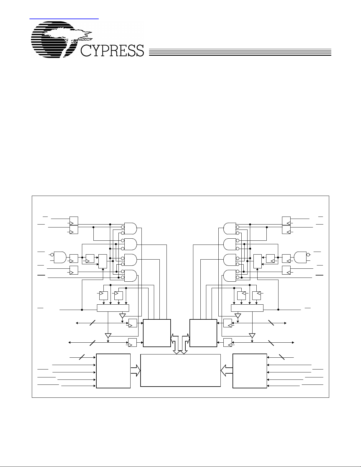
Logic Block Diagram
R/W
L
UB
L
CE
0L
CE
1L
LB
L
OE
L
FT/Pipe
I/O
I/O0L–I/O
A0L–A
CLK
ADS
CNTEN
CNTRST
L
[2]
–I/O
8/9L
15/17L
[3]
7/8L
[4] [4]
14/15L
L
L
L
L
8/9
8/9
15/16
1
0
0/1
1b
0b 1a 0a
0/1
ba
Counter/
Address
Register
Decode
I/O
Control
True Dual-Ported
RAM Array
I/O
Control
0/1
1b
0b1a0a
ba
Counter/
Address
Register
Decode
R/W
R
UB
R
CE
1
0
0/1
8/9
I/O
–I/O
8/9R
8/9
I/O0R–I/O
15/16
A0R–A
CNTRST
CE
LB
OE
FT/Pipe
[2]
15/17R
[3]
7/8R
14/15R
CLK
ADS
CNTEN
0R
1R
R
R
R
R
R
R
R
Notes:
1. See page 6 for Load Conditions.
–I/O15 for x16 devices; I/O9–I/O17 for x18 devices.
2. I/O
8
3. I/O
–I/O7 for x16 devices. I/O0–I/O8 for x18 devices.
0
4. A
for 32K; A0–A15 for 64K devices.
0–A14
For the most recent information, visit the Cypress web site at www.cypress.com
Cypress Semiconductor Corporation • 3901 North First Street • San Jose • CA 95134 • 408-943-2600
Document #: 38-06040 Rev. ** Revised September 19, 2001
CY7C09279/89
CY7C09379/89
Functional Description
The CY7C09279/89 and CY7C09379/89 are high-speed synchronous CMOS 32K, an d 64K x 16 /18 dual-p ort static RAMs.
Two po rts are prov ided, permitting i ndependent, s imultaneou s
access for reads and writes to any loca tion in mem ory.
[5]
Registers on control, address, a nd data li nes allow fo r minimal setup and hold times. In pipelin ed output mode, data is registered
for decreased cycle time. Clock to data valid t
(pipelined). Flow-through mode can also be used to bypass
CD2
= 6.5 ns
[1]
the pipelined output register to eliminate access latency. In
flow-through mode da ta will be avail able t
address is clocked into the device. Pipelined output or flowthrough mode is selected via the FT
/PIPE pin.
= 15 ns after the
CD1
Each port contains a bu rst co un ter on the i nput a ddress re gister. The internal write pulse width is independent of the LOWto-HIGH transition of the cl ock si gn al. The internal write puls e
is self-timed to allow the shortest possible cycle times.
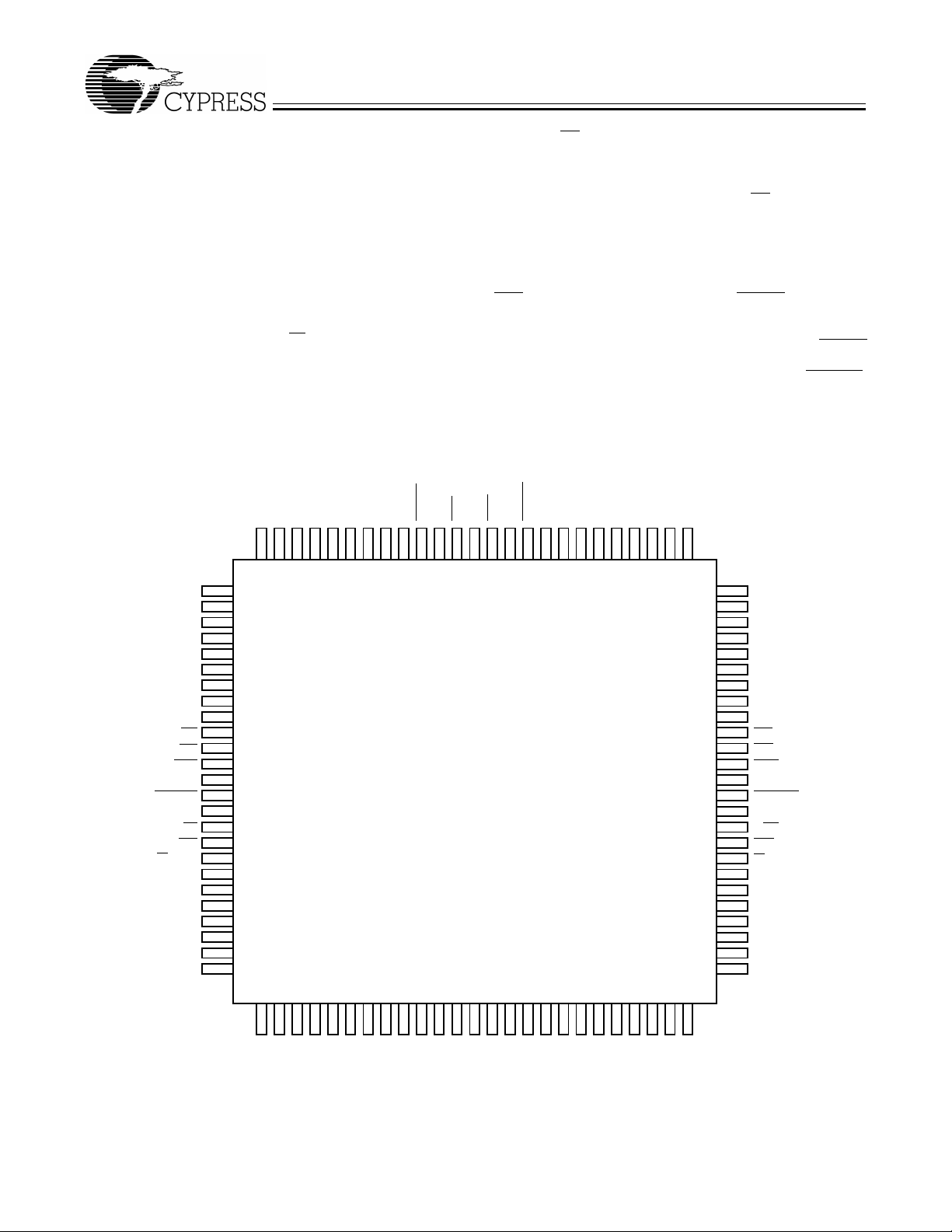
Pin Configurations
100-Pin TQFP (Top View)
A8L
A7L
A6L
A5L
A4L
CNTRSTL
[7]
FT/PIPEL
A10L
A11L
A12L
A13L
A14L
A15L
UBL
CE0L
CE1L
VCC
R/WL
OEL
GND
I/O15L
I/O14L
I/O13L
I/O12L
I/O11L
I/O10L
A9L
NC
NC
LBL
A3L
A1L
A2L
1
2
3
4
5
6
7
8
9
10
11
12
13
14
15
16
17
18
19
20
21
22
23
24
25
CY7C09289 (64K x 16)
CY7C09279 (32K x 16)
3332313029282726
CLKL
CNTENL
A0L
92 91 90 848587 868889 83 82 81 7678 77798093949596979899100
34 35 36 424139 403837 43 44 45 5048 494746
A HIGH on CE
down the internal circ uitry to reduce the static power consump-
or LOW on CE1 for one clock cycl e will po wer
0
tion. The use of multiple Chip Enables allows easier banking
of multiple chips for depth expansion configurations. In the
pipelined mode, one c ycl e is req uired wi th CE
HIGH to reactivate the outputs.
LOW and CE
0
Counter enable input s are provided to s tall the operation of the
address input and uti lize the internal address generated b y the
internal counter for fast interleaved memory applications. A
port’s burst counter is loaded with the port’s Address Strobe
). When the port’s Count Enable (CNTEN) is asserted,
(ADS
the address counter will increment on each LOW-to-HIGH
transition of that port’s clock signal. This will read/write one
word from/into each successive address location until CNTEN
is deasserted. The counter can address the entire memory
array and will loop back to the start. Counter Reset (CNTRST
is used to reset the burst counter.
All parts are available in 100-pin Thin Quad Plastic Flatpack
(TQFP) packages.
GND
ADSR
ADSL
CLKR
CNTENR
A0R
A1R
A2R
A3R
A4R
A5R
A6R
A7R
A8R
75
74
73
72
71
70
69
68
67
66
65
64
63
62
61
60
59
58
57
56
55
54
53
52
51
A9R
A10R
A11R
A12R
A13R
A14R
[6][6]
A15R
NC
NC
LBR
UBR
CE0R
CE1R
CNTRSTR
GND
R/WR
OER
FT/PIPER
GND
I/O15R
I/O14R
I/O13R
I/O12R
I/O11R
I/O10R
1
)
[7]
VCC
I/O7L
I/O8L
Notes:
5. When writing simultaneously to the same location, the final value cannot be guaranteed.
6. This pin is NC for CY7C09279.
7. For CY7C09279, pin #18 connected to V
through device.
I/O9L
is equivalent to an IDT x16 pipelined device; connecting pin #18 and #58 to GND is equivalent to an IDT x16 flow-
CC
I/O4L
I/O5L
I/O6L
GND
I/O2L
I/O3L
GND
I/O0L
I/O1L
I/O0R
I/01R
I/O4R
I/O2R
I/O3R
VCC
I/O7R
I/O6R
I/O5R
NC
I/O9R
I/O8R
Document #: 38-06040 Rev. ** Page 2 of 18
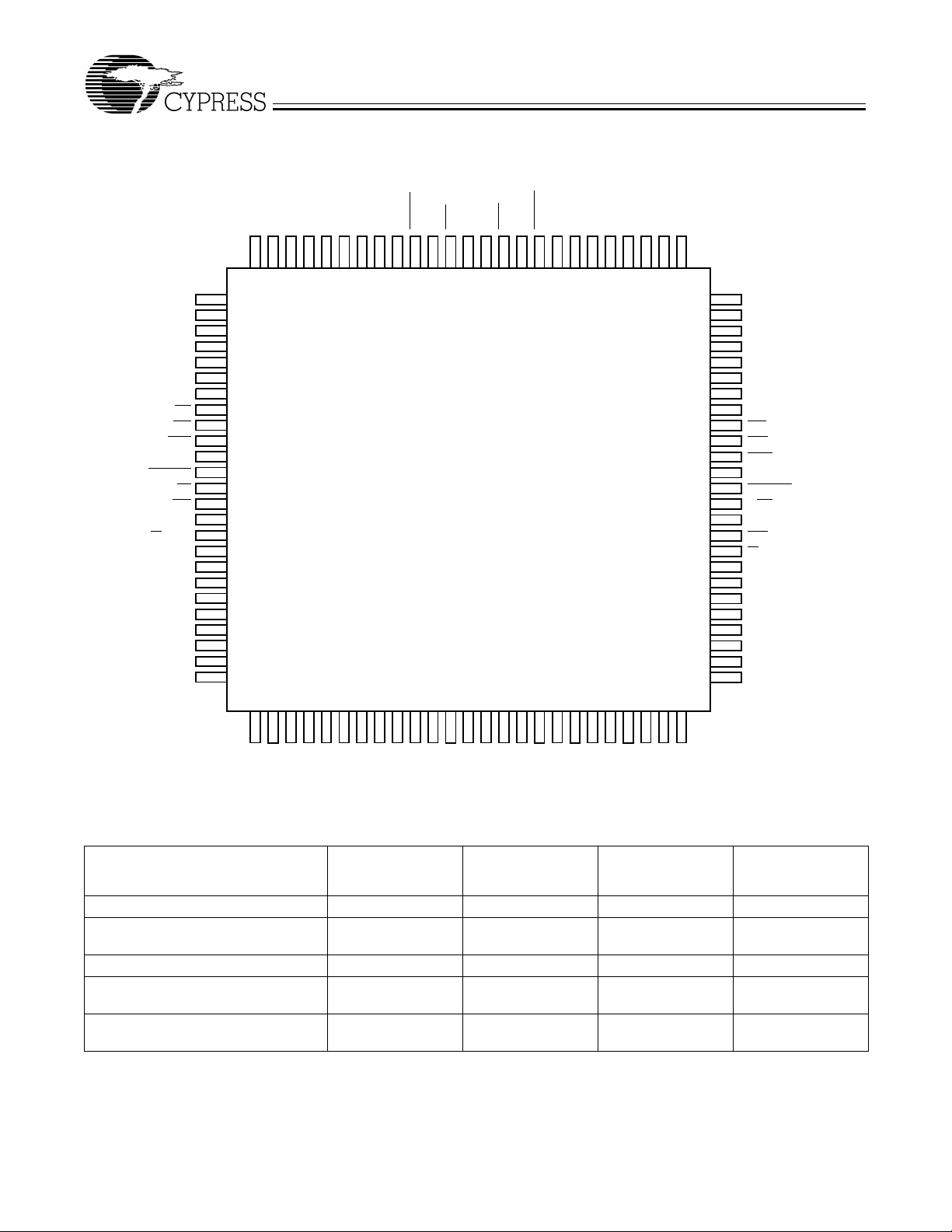
Pin Configurations (continued)
A8L
A7L
A6L
A9L
A10L
A11L
A12L
A13L
A14L
A15L
LBL
UBL
CE0L
CE1L
CNTRSTL
R/WL
OEL
VCC
FT/PIPEL
I/O17L
I/O16L
GND
I/O15L
I/O14L
I/O13L
1/012L
I/O11L
I/O10L
[8]
1
2
3
4
5
6
7
8
9
10
11
12
13
14
15
16
17
18
19
20
21
22
23
24
25
100-Pin TQFP (Top View)
A5L
A4L
A3L
A1L
A2L
CLKL
CNTENL
A0L
92 91 90 848587 868889 83 82 81 7678 77798093949596979899100
GND
ADSL
CY7C09389 (64K x 18)
CY7C09379 (32K x 18)
34 35 36 424139 403837 43 44 45 5048 494746
3332313029282726
GND
CY7C09279/89
CY7C09379/89
CNTENR
CLKR
A0R
A1R
A2R
A3R
A4R
A5R
A6R
A7R
75
74
73
72
71
70
69
68
67
66
65
64
63
62
61
60
59
58
57
56
55
54
53
52
51
A8R
A9R
A10R
A11R
A12R
A13R
A14R
[8]
A15R
LBR
UBR
CE0R
CE1R
CNTRSTR
R/WR
GND
OER
FT/PIPER
I/O17R
GND
I/O16R
I/O15R
I/O14R
I/O13R
I/O12R
I/O11R
ADSR
I/O9L
I/O8L
VCC
I/O7L
I/O6L
I/O5L
I/O4L
I/O3L
I/O2L
GND
I/O1L
I/O0L
GND
I/O0R
I/01R
I/O2R
I/O3R
I/O4R
I/O5R
I/O6R
VCC
I/O7R
I/O8R
I/O9R
I/10R
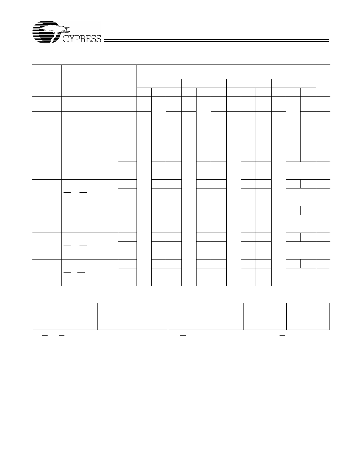
Selection Guide
CY7C09279/89
CY7C09379/89
(MHz) (Pipelined) 100 83 67 50
f
MAX2
Max Access Time (ns)
[1]
-6
6.5 7.5 9 12
(Clock to Data, Pipelined)
Typical Operating Current I
Typical Standby Current for I
(Both Ports TTL Level)
Typical Standby Current for I
(Both Ports CMOS Level)
Note:
8. This pin is NC for CY7C09379.
(mA) 250 235 215 195
CC
SB1
SB3
(mA)
(mA)
45 40 35 30
0.05 0.05 0.05 0.05
Document #: 38-06040 Rev. ** Page 3 of 18
CY7C09279/89
CY7C09379/89
-7
CY7C09279/89
CY7C09379/89
-9
CY7C09279/89
CY7C09379/89
-12
Pin Definitions
Left Port Right Port Description
A0L–A
15L
ADS
L
CE0L,CE
CLK
L
CNTEN
L
CNTRST
I/O0L–I/O
LB
L
UB
L
OE
L
R/W
L
FT/PIPE
GND Ground Input.
NC No Connect.
V
CC
L
1L
L
17L
A0R–A
15R
ADS
R
CE0R,CE
CLK
R
CNTEN
CNTRST
I/O0R–I/O
LB
R
UB
R
OE
R
R/W
R
FT/PIPE
Address Inputs (A0–A
for 32K, A0–A
14
for 64K devices).
15
Address Strobe Input. Used as an address qualifier. This signal should be asserted LOW to
access the part usin g an exter nally supplied address. Ass erting this s ignal LOW a lso loads t he
burst counter with the address present on the address pins.
Chip Enable Input. To select either the left or right port, both CE0 AND CE1 must be asserted
1R
to their active states (CE0 ≤ VIL and CE1 ≥ VIH).
Clock Signal. This input can be free running or strobed. Maximum clock input rate is f
R
Counter Enable Input. Asserting this signal LOW increments the burst address counter of its
respective port on each risi ng edge of CLK. CNTEN
LOW.
Counter Reset Input. As serting this s ignal LO W res ets th e burst a ddress counter of its respe c-
R
tive port to zero. CNTRST is not disabled by asserting ADS or CNTEN.
Data Bus Input/Output (I/O0–I/O15 for x16 devices).
17R
Lower Byte Select Input. Asserting this signal LOW enables read and write operations to the
lower byte. (I/O
and OE signals must be asserted t o drive output data on the lowe r byte o f the da ta pins.
the LB
–I/O8 for x18, I/O0–I/O7 for x16) of the memory array . For read operations both
0
Upper Byte Select Input. Same function as LB, but to the upper byte (I/O
Output Enable Input. This signa l must be asserted LOW to enable the I/O da ta pins during read
operations.
Read/Write Enable Inp ut. Thi s s ign al is asserte d LO W to write t o the du al po rt me mo ry arra y.
For read operations, assert this pin HIGH.
Flow-Through/Pipelined Select Input. For flow-through mode operation, assert this pin LOW.
R
For pipelined mode operation, assert this pin HIGH.
Power Input.
CY7C09279/89
CY7C09379/89
.
MAX
is disabled if ADS or CNTRST are asserted
8/9L
–I/O
15/17L
).
Maximum Ratings
(Above which the useful life may be im pai red. For user guidelines, not tested.)
Storage Temperature................................. –65
Ambient Temperature with Power Applied..–55°C to +125°C
Supply Voltage to Ground Potential...............–0.3V to +7.0V
DC Voltage Applied to
Outputs in High Z State.................................–0.5V to +7.0V
DC Input Voltage............................................–0.5V to +7.0V
Note:
9. Industrial parts are available in CY7C09289 and Cy7C09389 only
°C to +150°C
Output Current into Outputs (LOW).............................20 mA
Static Discharge Voltage ...........................................>1100V
Latch-Up Current.....................................................>200 mA
Operating Range
Range
Commercial 0°C to +70°C 5V ± 10%
Industrial
[9]
Ambient
Temperature V
CC
–40°C to +85°C 5V ± 10%
Document #: 38-06040 Rev. ** Page 4 of 18
Electrical Characteristics Ov er the Op erat ing Range
[1]
-6
Parameter Description
V
V
V
V
I
OZ
I
CC
I
SB1
OH
OL
IH
IL
Output HIGH Voltage
= Min., IOH= –4.0 mA)
(V
CC
Output LOW V o lta ge
(VCC= Min., IOH= +4.0 mA)
Input HIGH Vo ltage 2.2 2.2 2.2 2.2 V
Input LOW Voltage 0.8 0.8 0.8 0.8 V
Output Leakage Current –10 10 –10 10 –10 10 –10 10 µA
Operating Current
=Max.,
(V
CC
=0mA)
I
OUT
Outputs Disabled
Standby Current (Both
Ports TTL Level)
[10]
CEL & CER ≥ VIH,
f=f
MAX
I
SB2
Standby Current (One
Port TTL Level)
[10]
CEL | CER ≥ VIH,
f=f
MAX
I
SB3
I
SB4
Standby Current (Both
Ports CMOS Level)
CEL & CER ≥ V
0.2V, f = 0
Standby Current (One
Port CMOS Level)
CC
[10]
–
[10]
CEL | CER ≥ VIH,
f=f
MAX
Com’l. 250 450 235 420 215 360 195 300 mA
Ind.
Com’l. 45 115 40 105 35 95 30 85 mA
Ind.
Com’l. 175 235 160 220 145 205 125 190 mA
Ind.
Com’l. 0.05 0.5 0.05 0.5 0.05 0.5 0.05 0.5 mA
Ind.
Com’l. 160 200 145 185 130 170 110 150 mA
Ind.
Min. Typ. Max. Min. Typ. Max. Min. Typ. Max. Min. Typ. Max.
2.4 2.4 2.4 2.4 V
[9]
[9]
[9]
[9]
[9]
CY7C09279/89
CY7C09379/89
CY7C09279/89
CY7C09379/89
-7 -9 -12
Unit
0.4 0.4 0.4 0.4 V
245 410 mA
50 110 mA
160 220 mA
0.05 0.5 mA
145 185 mA
Capacitance
Parameter Description Test Conditions Max. Unit
C
IN
C
OUT
Note:
and CER are internal signals. To select either the left or right port, both CE0 AND CE1 must be asserted to their active states (CE0 ≤ VIL and CE1 ≥ VIH).
10. CE
L
Document #: 38-06040 Rev. ** Page 5 of 18
Input Capacitance TA = 25°C, f = 1 MHz,
Output Capacitance 10 pF
VCC = 5.0V
10 pF
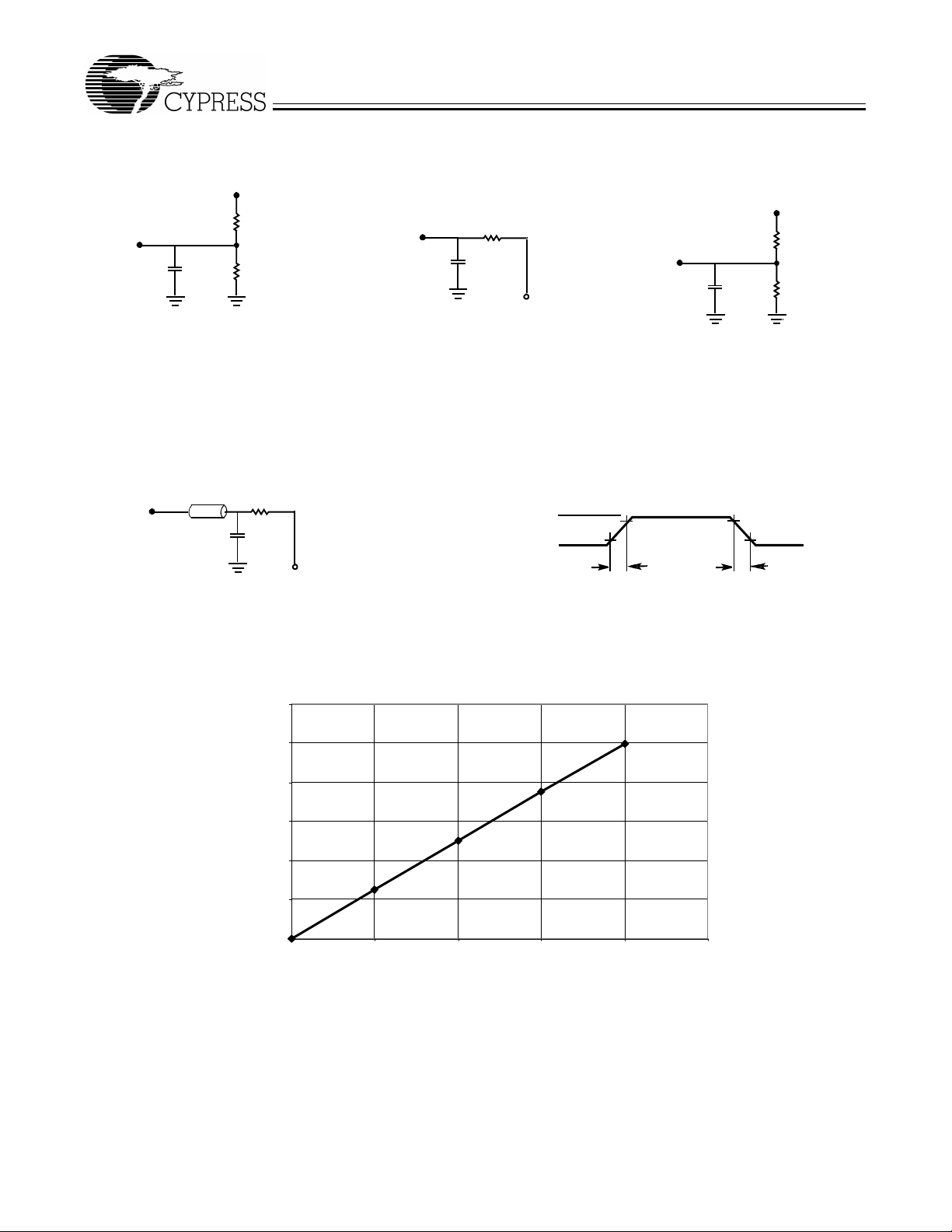
AC Test Loads
OUTPUT
C= 30pF
(a) Normal Load (Load 1)
5V
R1 = 893Ω
R2 = 347
CY7C09279/89
CY7C09379/89
5V
R
= 250Ω
OUTPUT
C=
30 pF
Ω
(b) Thévenin Equivalent (Load1)
TH
V
TH
=1.4V
OUTPUT
C= 5pF
(c)Three-State Delay(Load 2)
(Used for t
CKLZ
, t
OLZ
including scope and jig)
R1 = 893Ω
R2 = 347Ω
, & t
OHZ
AC Test Loads (Applicable to -6 only)
Z0 = 50
Ω
R = 50
OUTPUT
C
(a) Load 1 (-6 only)
Ω
VTH=1.4V
0.60
0.50
0.40
0.30
0.20
[11]
3.0V
GND
≤
3ns
ALL INPUTPULSES
10%
90%
90%
10%
ns
3
≤
0.1 0
(ns) for all -12 access ti mes
∆
0.00
1 0 1 5 20 25 30 35
Capacitance (pF)
(b) Load Derating Curve
Note:
11. Test Conditions: C = 10 pF.
Document #: 38-06040 Rev. ** Page 6 of 18

Switching Characteristics Over the Operating Range
Parameter Description
f
f
MAX1
f
MAX2
t
CYC1
t
CYC2
t
CH1
t
CL1
t
CH2
t
CL2
t
R
t
F
t
SA
t
HA
t
SC
t
HC
t
SW
t
HW
t
SD
t
HD
t
SAD
t
HAD
t
SCN
t
HCN
t
SRST
t
HRST
t
OE
[12, 13]
t
OLZ
[12, 13]
t
OZ
t
CD1
t
CD2
t
DC
[12, 13]
t
CKHZ
[12, 13]
t
CKLZ
Port to Port Delays
t
CWDD
t
CCS
Notes:
12. Test conditions used are Load 2.
13. This parameter is guaranteed by design, but it is not production tested.
Flow-Through 53 45 40 33 MHz
Max
f
Pipelined 100 83 67 50 MHz
Max
Clock Cycle Tim e - Flow-Throu gh 19 22 25 30 ns
Clock Cycle Tim e - Pipelin ed 10 12 15 20 ns
Clock HIGH Tim e - Flow-Through 6.5 7.5 12 12 ns
Clock LOW Time - Flow-Through 6.5 7.5 12 12 ns
Clock HIGH Time - Pipelined 4568ns
Clock LOW Time - Pipelined 4568ns
Clock Rise Time 3333ns
Clock Fall Time 3333ns
Address Set-Up Time 3.5 4 4 4 ns
Address Hold Time 0011ns
Chip Enable Set-Up Time 3.5 4 4 4 ns
Chip Enable Hold Time 0011ns
R/W Set-Up Time 3.5 4 4 4 ns
R/W Hold Time 0011ns
Input Data Set-Up Time 3.5 4 4 4 ns
Input Data Hold Time 0011ns
ADS Set-Up Time 3.5 4 4 4 ns
ADS Hold Time 0011ns
CNTEN Set-Up Time 3.5444ns
CNTEN Hold Time 0011ns
CNTRST Set-Up Time 3.5 4 4 4 ns
CNTRST Hold Time 0011ns
Output Enable to Data Valid 8 9 10 12 ns
OE to Low Z 2222ns
OE to High Z 17171717ns
Clock to Data Valid - Flow-Through 15 18 20 25 ns
Clock to Data Valid - Pipelined 6.5 7.5 9 12 ns
Data Output Hold After Clock HIGH2222ns
Clock HIGH to Output High Z 29292929ns
Clock HIGH to Output Low Z 2222ns
Write Port Clock HIGH to Read Data Delay 30 35 40 40 ns
Clock to Clock Set-Up Time 9 10 15 15 ns
CY7C09279/89
CY7C09379/89
CY7C09279/89
CY7C09379/89
[1]
-6
Min. Max. Min. Max. Min. Max. Min. Max.
-7 -9 -12
Unit
Document #: 38-06040 Rev. ** Page 7 of 18

Switching Waveforms
Read Cycle for Flow-Through Output (FT/PIPE = VIL)
t
CYC1
CLK
CE
CE
t
CH1
0
t
SC
1
t
HC
t
CL1
[14, 15, 16, 17]
CY7C09279/89
CY7C09379/89
t
SC
t
HC
R/W
ADDRESS
DATA
OUT
t
t
SW
SA
t
HW
t
HA
A
n
t
CD1
t
CKLZ
A
n+1
OE
Read Cycle for Pipelined Operation (FT/PIPE = VIH)
t
CYC2
CLK
CE
CE
t
CH2
0
t
SC
1
t
HC
t
CL2
t
DC
Q
n
[14, 15, 16, 17]
A
n+2
Q
n+1
t
OHZ
A
n+3
t
CKHZ
Q
n+2
t
t
OLZ
t
OE
t
SC
DC
t
HC
R/W
ADDRESS
DATA
OUT
t
SW
t
SA
t
HW
t
HA
A
n
1 Latency
t
CKLZ
A
n+1
t
CD2
A
n+2
t
DC
Q
n
A
n+3
Q
n+1
t
OHZ
t
OLZ
Q
n+2
OE
t
OE
Notes:
is asynchronously controlled; all other inputs are synchronous to the rising clock edge.
14. OE
= VIL, CNTEN and CNTRST = VIH.
15. ADS
16. The output is disabled (high-impedance state) by CE
17. Addresses do not have to be accessed sequentially since ADS
or CE1 = VIL following the next rising edge of the clock.
0=VIH
= VIL constantly loads the address on the rising edge of the CLK. Numbers are for reference only.
Document #: 38-06040 Rev. ** Page 8 of 18

Switching Waveforms (continued)
Bank Select Pipelined Read
CLK
L
t
SA
ADDRESS
CE
(B1)
0(B1)
t
SC
[18, 19]
t
CYC2
t
CH2
A
0
t
CL2
t
HA
t
HC
CY7C09279/89
CY7C09379/89
A
1
t
CD2
A
2
t
t
t
SC
HC
CD2
A
3
t
CKHZ
A
4
t
CD2
A
5
t
CKHZ
DATA
OUT(B1)
ADDRESS
CE
DATA
OUT(B2)
(B2)
0(B2)
t
SA
A
t
SC
t
HA
0
t
HC
A
1
Left Port Write to Flow-Through Right Port Read
CLK
L
R/W
L
ADDRESS
ADDRESS
DATA
Notes:
18. In this depth expansion example, B1 represents Bank #1 and B2 is Bank #2; each Bank consists of one Cypress dual-port device from this data sheet.
ADDRESS
19. UB
20. The same waveforms apply for a right port write to flow-through left port read.
21. CE
22. OE
23. It t
until t
L
DATA
INL
CLK
R
R/W
R
R
OUTR
(B1)
, LB, OE and ADS = VIL; CE
, UB, LB, and ADS = VIL; CE1, CNTEN, and CNTRST = VIH.
0
= VIL for the right port, which is being read from. OE = VIH for the left port, which is being written to.
≤ maximum specified, then data from right port READ is not valid until the maximum specified for t
CCS
+ t
CCS
CD1
t
SW
t
SA
MATCH
t
SD
= ADDRESS
. t
CWDD
(B2)
does not apply in this case.
VALID
.
1(B1)
t
CCS
t
SWtHW
t
SAtHA
MATCH
t
DC
, CE
1(B2)
t
HW
t
HA
t
HD
t
CWDD
, R/W, CNTEN, and CNTRST = VIH.
D
t
SC
[20, 21, 22, 23]
t
CD1
0
t
DC
A
2
t
HC
D
1
NO
MATCH
t
DC
A
3
t
CKLZ
NO
MATCH
t
CD2
t
CD1
t
CKLZ
A
4
t
CKHZ
D
2
VALID VALID
t
DC
. If t
CWDD
>maximum specified, then data is not valid
CCS
D
3
A
5
t
CD2
t
CKLZ
D
4
Document #: 38-06040 Rev. ** Page 9 of 18

Switching Waveforms (continued)
Pipelined Read-to-Write-to-Read (OE
t
CYC2
t
CL2
t
HC
CLK
CE
CE
t
CH2
0
t
SC
1
= VIL)
[17, 24, 25, 26]
t
SW
t
CY7C09279/89
CY7C09379/89
HW
R/W
t
HW
n
t
HA
A
n+1
t
CD2
ADDRESS
DATA
DATA
OUT
t
SW
A
t
SA
IN
Pipelined Read-to-Write-to-Read (OE Controlled)
t
CYC2
t
CL2
t
HC
t
HW
CLK
CE
CE
R/W
t
CH2
0
t
SC
1
t
SW
A
n+2
t
CKHZ
Q
n
NO OPERATION WRITEREAD READ
[17, 24, 25, 26]
t
t
HW
SW
A
n+2
tSDt
D
n+2
HD
A
n+3
t
CKLZ
A
n+4
t
CD2
Q
n+3
A
n
A
n+1
A
n+2
A
n+3
A
n+4
A
n+5
ADDRESS
t
HA
t
CD2
Q
n
t
OHZ
tSDt
D
n+2
HD
D
n+3
t
CKLZ
t
CD2
Q
n+4
DATA
DATA
OUT
t
SA
IN
OE
READ READWRITE
Notes:
24. Output state (HIGH, LOW, or High-Impedance) is determined by the previous cycle control signals.
and ADS = VIL; CE1, CNTEN, and CNTRST = VIH.
25. CE
0
26. During “No Operation,” data in memory at the selected address may be corrupted and should be rewritten to ensure data integrity.
Document #: 38-06040 Rev. ** Page 10 of 18

Switching Waveforms (continued)
Flow-Through Read-to-Write-to-Read (OE
t
CYC1
CLK
CE
CE
R/W
ADDRESS
DATA
t
CH1
0
t
SC
1
t
SW
A
n
t
SA
IN
t
CD1
t
t
HC
HW
t
HA
t
CL1
A
n+1
= VIL)
t
CD1
[15, 17, 24, 25]
A
n+2
CY7C09279/89
CY7C09379/89
t
SW
A
n+2
t
SD
D
n+2
t
t
HW
HD
A
n+3
t
CD1
A
n+4
t
CD1
DATA
OUT
Q
n
t
DC
t
CKHZ
READ
Flow-Through Read-to-Write-to-Read (OE Controlled)
t
CYC1
CLK
CE
CE
R/W
ADDRESS
DATA
DATA
OUT
OE
t
CH1
0
t
SC
1
t
SW
A
n
t
SA
IN
t
CD1
t
t
HC
HW
t
HA
t
CL1
t
SW
A
n+1
t
SD
t
DC
Q
n
t
OHZ
READ
Q
n+1
OPERATION
[15, 17, 24, 25]
A
n+2
D
n+2
NO
t
HW
t
HD
A
D
WRITE READ
n+3
n+3
A
n+4
t
WRITE READ
t
CKLZ
OE
t
t
CKLZ
CD1
Q
n+3
t
DC
A
n+5
t
CD1
Q
n+4
t
DC
Document #: 38-06040 Rev. ** P age 11 of 18

Switching Waveforms (continued)
Pipelined Read with Address Counter Advance
t
CYC2
CLK
t
CH2
t
CL2
CY7C09279/89
CY7C09379/89
[27]
ADDRESS
t
t
SAD
SA
A
t
HA
n
t
HAD
ADS
CNTEN
DATA
OUT
t
SCN
Q
x-1
READ
EXTERNAL
t
HCN
t
CD2
Q
x
t
DC
READ WITH COUNTER
ADDRESS
Flow-Through Read with Address Counter Advance
t
CYC1
CLK
ADDRESS
t
CH1
t
SA
A
n
t
CL1
t
HA
Q
n
[27]
t
SAD
t
SCN
t
HAD
t
HCN
Q
n+1
COUNTER HOLD
Q
n+2
READ WITH COUNTER
Q
n+3
t
SAD
t
HAD
ADS
t
SAD
t
HAD
CNTEN
t
SCN
DATA
OUT
Note:
and OE = VIL; CE1, R/W and CNTRST = VIH.
27. CE
0
Q
t
HCN
t
CD1
x
t
DC
READ
EXTERNAL
ADDRESS
t
SCN
Q
n
Q
n+1
Q
n+2
READ WITH COUNTER
t
HCN
Q
n+3
COUNTER HOLD
READ
WITH
COUNTER
Document #: 38-06040 Rev. ** Page 12 of 18

Switching Waveforms (continued)
Write with Address Counter Advance (Flow-Through or Pipelined Outputs)
t
CYC2
CLK
ADDRESS
t
CH2
t
SA
A
n
t
CL2
t
HA
CY7C09279/89
CY7C09379/89
[28, 29]
INTERNAL
ADDRESS
t
SAD
t
HAD
A
n
ADS
CNTEN
t
SCN
DATA
IN
t
SD
WRITE EXTERNAL
Notes:
, UB, LB, and R/W = VIL; CE1 and CNTRST = VIH.
28. CE
0
29. The “Internal Address” is equal to the “External Address” when ADS
D
n
ADDRESS
t
HCN
t
HD
D
n+1
WRITE WITH
COUNTER
A
n+1
D
n+1
WRITE COUNTER
HOLD
= VIL and equals the counter output when ADS = VIH.
D
n+2
A
n+2
D
n+3
WRITE WITH COUNTER
A
n+3
D
n+4
A
n+4
Document #: 38-06040 Rev. ** Page 13 of 18

Switching Waveforms (continued)
CYC2
[17, 29, 30, 31]
t
CL2
Counter Reset (Pipelined Outputs)
t
t
CH2
CLK
t
SAtHA
CY7C09279/89
CY7C09379/89
ADDRESS
INTERNAL
ADDRESS
A
X
t
SWtHW
01A
R/W
t
SAD
t
HAD
ADS
t
SCN
t
HCN
CNTEN
t
SRST
CNTRST
DATA
IN
DATA
OUT
Notes:
, UB, and LB = VIL; CE1 = VIH.
30. CE
0
31. No dead cycle exists during counter reset. A READ or WRITE cycle may be coincidental with the counter reset.
t
HRST
COUNTER
RESET
t
SDtHD
D
0
WRITE
ADDRESS 0
READ
ADDRESS 0
READ
ADDRESS 1
Q
0
A
n
n
READ
ADDRESS n
A
n+1
A
n+1
Q
1
Q
n
Document #: 38-06040 Rev. ** Page 14 of 18

CY7C09279/89
CY7C09379/89
Read/Write and Enable Operation
[32, 33, 34]
Inputs Outputs
OE CLK CE
0
CE
1
R/W I/O0–I/O
17
X H X X High-Z Deselected
X X L X High-Z Deselected
X L H L D
L L H H D
IN
OUT
Write
Read
H X L H X High-Z Outputs Disabled
Address Counter Control Operation
[32, 36, 37, 38]
Previous
Address
X X X X L D
A
X A
X A
Address CLK ADS CNTEN CNTRST I/O Mode Operation
out(0)
n
X L X H D
n
n
H H H D
H L H D
out(n)
out(n)
out(n+1)
Reset Counter Reset to Address 0
Load Address Load into Counter
Hold External Address Blocked—Counter
Disabled
Increment Counter Enabled—Internal Address
Generation
Operation
[35]
[35]
[34]
Notes:
32. “X” = “Don’t Care,” “H” = V
33. ADS
34. OE
35. When CE
36. CE
37. Data shown for flow-through mode; pipelined mode output will be delayed by one cycle.
38. Counter operation is independent of CE
, CNTEN, CNTRST = “Don’t Care.”
is an asynchronous input signal.
changes state in the pipelined mode, deselection and read happen in the following clock cycle.
and OE = VIL; CE1 and R/W = VIH.
0
, “L” = VIL.
IH
and CE1.
0
Document #: 38-06040 Rev. ** Page 15 of 18

CY7C09279/89
CY7C09379/89
Ordering Information
32K x16 Synchronous Dual-Port SRAM
Speed
(ns) Ordering Code
[1]
6.5
7.5 CY7C09279-7AC A100 100-Pin Thin Quad Flat Pack Commercial
9 CY7C09279-9AC A100 100-Pin Thin Quad Flat Pack Commercial
12 CY7C09279-12AC A100 100-Pin Thin Quad Flat Pack Commercial
64K x16 Synchronous Dual-Port SRAM
Speed
(ns) Ordering Code
6.5
7.5 CY7C09289-7AC A100 100-Pin Thin Quad Flat Pack Commercial
9 CY7C09289-9AC A100 100-Pin Thin Quad Flat Pack Commercial
12 CY7C09289-12AC A100 100-Pin Thin Quad Flat Pack Commercial
CY7C09279-6AC A100 100-Pin Thin Quad Flat Pack Commercial
[1]
CY7C09289-6AC A100 100-Pin Thin Quad Flat Pack Commercial
CY7C09289-9AI A100 100-Pin Thin Quad Flat Pack Industrial
Package
Name Package Type
Package
Name Package Type
Operating
Range
Operating
Range
32K x18 Synchronous Dual-Port SRAM
Speed
(ns) Ordering Code
[1]
6.5
7.5 CY7C09379-7AC A100 100-Pin Thin Quad Flat Pack Commercial
9 CY7C09379-9AC A100 100-Pin Thin Quad Flat Pack Commercial
12 CY7C09379-12AC A100 100-Pin Thin Quad Flat Pack Commercial
64K x18 Synchronous Dual-Port SRAM
Speed
(ns) Ordering Code
6.5
7.5 CY7C09389-7AC A100 100-Pin Thin Quad Flat Pack Commercial
9 CY7C09389-9AC A100 100-Pin Thin Quad Flat Pack Commercial
12 CY7C09389-12AC A100 100-Pin Thin Quad Flat Pack Commercial
CY7C09379-6AC A100 100-Pin Thin Quad Flat Pack Commercial
[1]
CY7C09389-6AC A100 100-Pin Thin Quad Flat Pack Commercial
CY7C09389-9AI A100 100-Pin Thin Quad Flat Pack Industrial
Package
Name Package Type
Package
Name Package Type
Operating
Range
Operating
Range
Document #: 38-06040 Rev. ** Page 16 of 18

ng so indemnifies Cypress Semiconductor against all charges.
Package Diagram
CY7C09279/89
CY7C09379/89
100-Pin Thin Plastic Quad Flat Pack (TQFP) A100
51-85048-B
Document #: 38-06040 Rev. ** Page 17 of 18
© Cypress Semiconductor Corporation, 2001. The information contained herein is subject to change without notice. Cypress Semiconductor Corporation assumes no responsibility for the use
of any circuitry other than circuitry embodied in a Cypress Semiconductor product. No r does it convey or imply any license under patent or other rights. Cypress Semiconductor does not autho rize
its products for use as critical components in life-support systems where a malfunction or failure may reasonably be expected to result in significant injury to the user. The inclusion of Cypress
Semiconductor products in life-support systems application implies that the manufacturer assume s all risk of such use and in doi

CY7C09279/89
CY7C09379/89
Document Title: CY7C09279/89, CY7C09379/89 32K/64K X 16/18 Synchronous Dual Port Static RAM
Document Number: 38-06040
REV. ECN NO.
** 110188 09/29/01 SZV Change from Spec number: 38-00664 to 38-06040
Issue
Date
Orig. of
Change Description of Change
Document #: 38-06040 Rev. ** Page 18 of 18
 Loading...