

1
查询CY7C09349A-6AC供应商
CY7C09349AV
CY7C09359AV
3.3V 4K /8K x 18
Synchronous Dual-Port Static RAM
Features
• True dual-ported memory cells which all ow simultaneous access of the same memory location
• Two Flow-Through/Pipelined devices
—4K x 18 organization (CY7C09349AV)
—8K x 18 organization (CY7C09359AV)
• Three Modes
—Flow-Through
—Pipelined
—Burst
• Pipelined outpu t mode on both ports allo ws fast 83-MHz
operation
• 0.35-micron CMOS for optimum speed/power
v
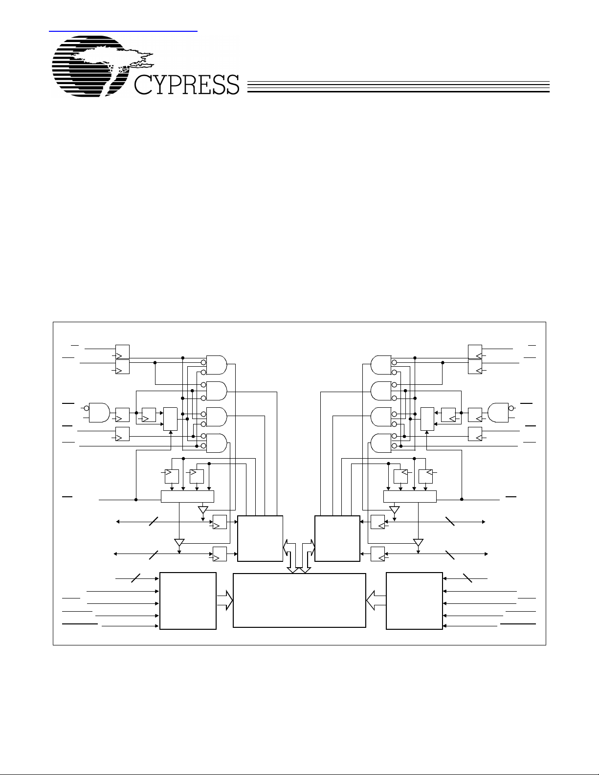
Logic Block Diagram
• High-speed clock to data access 9 and 12 ns (max.)
• 3.3V Low operating power
—A cti ve = 135 mA ( typi cal)
— Standby = 10 µA (typical)
• Fully synchronous int erf ace for easier operation
• Burst counters increment addresses internally
— Shorten cycle times
—Minimize bus noise
—Supported in Flow-Through and Pi peli ned m odes
• Dual Chip Enables f or easy depth expansi on
• Upper and lower byte controls for bus matching
• Aut omatic power-down
• Commercial and Industrial temperature ranges
Available in 100-pin TQFP
•
R/W
L
UB
L
CE
0L
CE
1L
LB
L
OE
L
FT/Pipe
I/O9L–I/O
I/O0L–I/O
A
CLK
ADS
CNTEN
CNTRST
L
17L
8L
[1] [1]
0L–A11/12L
L
L
L
12/13
L
0/1
9
9
1
0
0/1
1b
0b 1a 0a
ba
Counter/
Address
Register
Decode
I/O
Control
True Dual-Ported
RAM Array
I/O
Control
0/1
1b
0b1a0a
ba
Counter/
Address
Register
Decode
1
0
0/1
9
9
12/13
R/W
CE
CE
FT/Pipe
I/O9R–I/O
I/O0R–I/O
A0R–A
11/12R
CLK
ADS
CNTEN
CNTRST
UB
LB
OE
R
R
0R
1R
R
R
R
17R
8R
R
R
R
R
Notes:
1. A
for 4K; A0–A12 for 8K devices.
0–A11
For the most recent informati on, visit the Cypress web site at www .cypress. com
Cypress Semiconductor Corporation
• 3901 North First Street • San Jose • CA 95134 • 408-943-2600
Nove mber 13, 2000

CY7C09349AV
CY7C09359AV
Functional Description
A HIGH on CE
down the internal circu itry to reduce the static power consu mpThe CY7C09349AV and CY7C09359AV are high-speed 3.3V
synchronous CMOS 4K and 8K x 18 dual-port static RAMs.
Two ports are provide d, permitt ing i ndependent , si mul taneous
access for rea ds and writes to an y lo catio n in memory.
[2]
Registers on contr ol, addr ess, a nd data lin es allo w f o r mini mal setup and hold times . In pipelined out put mode, dat a is registere d
for decr ease d cycle t ime . Cloc k to dat a v ali d t
lined). Flow-through mode can also be used to bypass the
= 9 ns (pipe-
CD2
pipelined output register to eliminate access latency. In flowthrough mode data will be available t
dress is clocked into the device. Pipelined output or flowthrough mode is selected via the FT
= 18 ns after the ad-
CD1
/Pipe pin.
Each port contains a burs t co unter on the i nput address r egister. The internal write pulse width is indep endent of the LOWto-HIGH tra nsition of the clock signal . The internal write pulse
is self-t imed to allow the sho rtest possible cycle t ime s.
tion. The use of multiple Chip Enables allows easier banking
of multiple chips for depth expansion configurations. In the
pipelined mode, one cycle is required with CE
HIGH to reactivate the outputs.
Counter enabl e inputs are pro vided to sta ll the oper ation of the
address input an d utilize the internal address gener ated by t he
internal counter for fast interleaved memor y applications. A
port’s burst counter is loaded with the port’s Address Strobe
(ADS
the address counter will increment on each LOW-to-HIGH
transition of that port’s clock signal. This will read/write one
word from/into ea ch su cces siv e addres s locat ion unt il CNTEN
is deasserted. The counter can address the entire memory
array an d will loop back to the start. Counter Reset (CNTRST
is used to reset the burst counter.
All parts are available in 100-pin Thin Quad Plastic Flatpack
(TQFP) packages.
Note:
2. When simultaneously writing to the same location, final value cannot be guaranteed.
or LOW on CE1 for one clock cy cle will power
0
LOW and CE
0
). When the port’s Count Enable (CNTEN) is asserted,
1
)
2
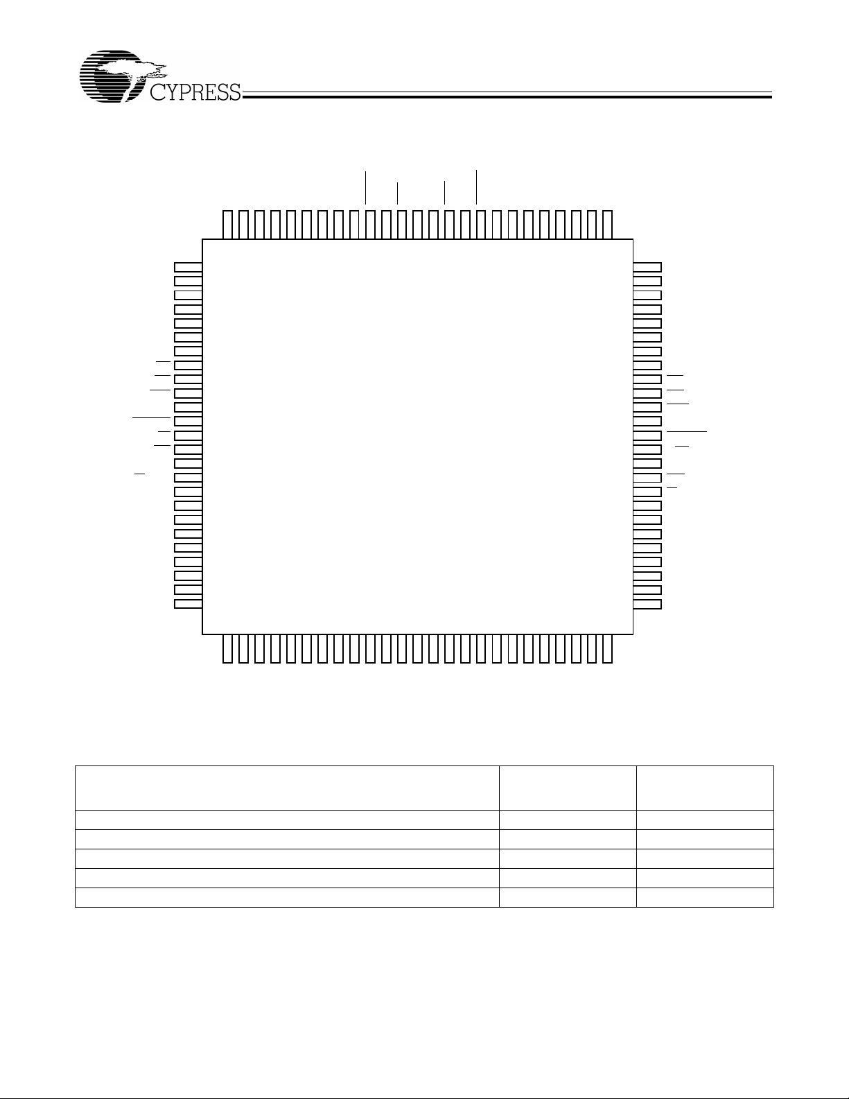
Pin Configuration
A9L
A10L
A11L
[3]
A12L
NC
NC
NC
LBL
UBL
CE0L
CE1L
CNTRSTL
R/WL
OEL
VCC
FT/PIPEL
I/O17L
I/O16L
GND
I/O15L
I/O14L
I/O13L
1/012L
I/O11L
I/O10L
CY7C09349AV
CY7C09359AV
100-Pin TQFP (Top View)
A8L
A7L
A6L
A5L
A4L
A3L
A1L
A2L
1
2
3
4
5
6
7
8
9
10
11
12
13
14
15
16
17
18
19
20
21
22
23
24
25
CY7C09359AV (8K x 18)
CY7C09349AV (4K x 18)
3332313029282726
CLKL
CNTENL
A0L
92 91 90 848587 868889 83 82 81 7678 77798093949596979899100
34 35 36 424139 403837 43 44 45 5048 494746
GND
GND
ADSL
ADSR
CNTENR
A0R
CLKR
A1R
A2R
A3R
A4R
A5R
A6R
A7R
75
74
73
72
71
70
69
68
67
66
65
64
63
62
61
60
59
58
57
56
55
54
53
52
51
A8R
A9R
A10R
A11R
[3]
A12R
NC
NC
NC
LBR
UBR
CE0R
CE1R
CNTRSTR
R/WR
GND
OER
FT/PIPER
I/O17R
GND
I/O16R
I/O15R
I/O14R
I/O13R
I/O12R
I/O11R
VCC
I/O7L
I/O8L
I/O9L
I/O4L
I/O5L
I/O6L
GND
I/O2L
I/O3L
GND
I/O0L
I/O1L
I/01R
I/O0R
I/O4R
I/O2R
I/O3R
VCC
I/O7R
I/O6R
I/O5R
I/10R
I/O9R
I/O8R
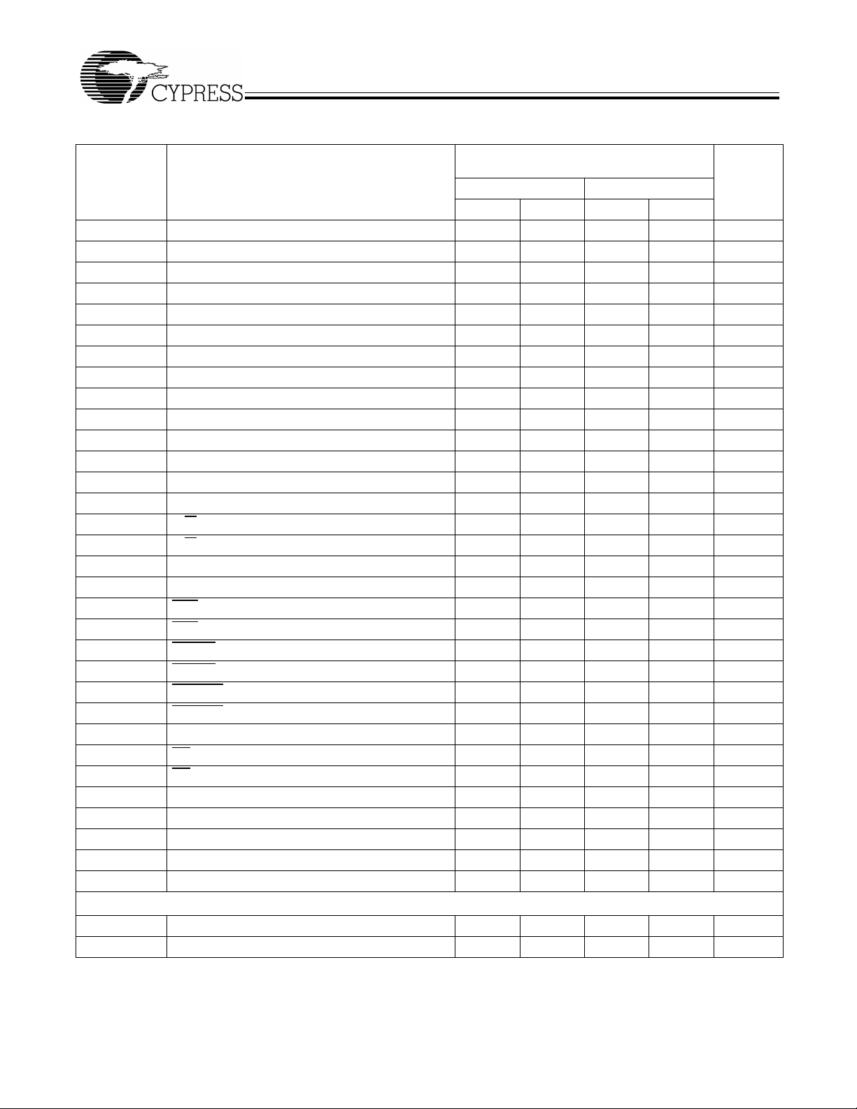
Selectio n Guide
CY7C09349AV
CY7C09359AV
-9
f
(MHz) (Pipelined) 67 50
MAX2
Max Access Time (ns) (Clock to Data, Pipelined) 9 12
Typical Operating Current I
Typical Standby Current for I
Typical Standby Current for I
Shaded areas contain advance information.
Note:
3. This pin is NC for CY7C09349AV.
(mA) 135 115
CC
(mA) (Both Ports TTL Level) 20 20
SB1
(µA) (Both P orts CMOS Lev el) 10 µA 10 µA
SB3
3
CY7C09349AV
CY7C09359AV
-12
Pin Definitions
Left Port Right Port Description
A0L–A
12L
ADS
L
CE0L,CE
CLK
L
CNTEN
L
CNTRST
I/O0L–I/O
LB
L
UB
L
OE
L
R/W
L
FT/PIPE
GND Ground Input.
NC No Connect.
V
CC
L
1L
L
17L
A0R–A
12R
ADS
R
CE0R,CE
CLK
R
CNTEN
CNTRST
I/O0R–I/O
LB
R
UB
R
OE
R
R/W
R
FT/PIPE
Address Inputs (A0–A
for 4K, A0–A
11
for 8K devices).
12
Address Strobe I nput. Used as an addr ess qualifier . This signal should be ass erted LOW during
normal read or write transactions. Asserting this signal LOW also loads the burst address
counter with data present on the I/O pins.
Chip Enable Inpu t. To select ei ther the left or right port, both CE0 AND CE1 must be asserted
1R
to their active states (C E
≤ VIL and CE1 ≥ VIH).
0
Clock Signal. This input can be free running or strobed. Maximum clock input rate is f
R
Counter Enable In put. Asserting this signal LOW increments the b urst address coun ter of it s
respectiv e port on each rising edge of CLK. CNTEN
LOW.
Counter Reset Input. Asserting thi s signal LO W resets t he burs t address count er of its res pec-
R
tive port to zero. CNTRST
Data Bus Input/Output (I/O0–I/O15 for x16 devi c es).
17R
is not disab led by asserting ADS or CNTEN.
Lower Byte Select Input. Asserting this signal LOW enables read and write oper ations to the
lower byte (I/O
the LB
and OE signals m ust be asserted to driv e out put dat a on the l ower b yte of the dat a pi ns.
–I/O8 for x18, I/O0–I/O7 for x16) of the memory arra y. For read oper ations both
0
Upper Byte Select Input. Same function as LB, but to the upper byte (I/O
Output Enable Input. Thi s signal must be ass erted LOW to enable t he I/O data pins during read
operations.
Read/Write Enable Input. This signal is asserted LOW to write to the dual port memory array.
For read operations, assert this pin HIGH.
Flow-Through/ Pipelined Select Input. For flow-through mode operation, assert this pin LOW.
R
For pipelined mode operation, assert this pin HIGH.
Power Input.
CY7C09349AV
CY7C09359AV
.
MAX
is disab led if ADS or CNTRST are as serted
8/9L
–I/O
15/17L
).
Maximum Ratings
(Abov e which the useful life may be impair ed. For user guidelines, not tested.)
Storage Temperature ............ .. .......... ... ...... –65
Ambient Temperature with
Power Applied .............................................–55
Supply Voltage to Gr o u nd Potent ia l ..... ......... . –0.5V to +4.6V
DC Voltage Applied to
Outputs in High Z State ...........................–0.5V to V
DC Input Voltage......................................–0.5V to V
Notes:
4. Industrial parts are available in CY7C09359AV only.
°
C to +150°C
°
C to +125°C
+0.5V
CC
+0.5V
CC
Output Current into Outputs (LOW)............................. 20 mA
Static Discharge Voltage .......... ............ ............ .........>2001V
Latch-Up Current .....................................................>200 mA
Operating Range
Range
Commercial 0°C to +70°C 3.3V ± 300 mV
Industrial
[4]
Ambient
Temperature V
CC
–40°C to +85°C 3.3V ± 300 mV
4
CY7C09349AV
CY7C09359AV
Electrical Characteristics
Over the Operating Range
Parameter Description
V
V
V
V
I
I
I
I
I
I
OH
OL
IH
IL
OZ
CC
SB1
SB2
SB3
SB4
Output HIGH Voltage (V
Output LOW Voltage (V
CC
= Min., I
CC
= Min., I
Input HIGH Voltage 2.0 2.0 V
Input LOW Voltage 0.8 0.8 V
Output Leakage Current –10 10 –10 10 µA
Operating Current (V
I
= 0 mA) Outputs Disabled
OUT
Standby Current (Both Ports TTL
[5]
Level)
CEL & CER ≥ VIH, f =f
CC
= Max.,
Standby Current (One Port TTL Lev el)
CE
≥ VIH, f =f
R
Standby Current (Bot h Ports CMOS
[5]
Level)
Standby Current (One Port CMOS
[5]
Level)
MAX
CEL & CER ≥ V
– 0.2V, f = 0
CC
CEL | CER ≥ VIH, f = f
MAX
MAX
CY7C09349AV
CY7C09359AV
-9 -12
Min. Typ. Max. Min. Typ. Max.
= –4.0 mA) 2.4 2.4 V
OH
= +4.0 mA) 0.4 0.4 V
OH
Com’l. 135 230 115 180 mA
Ind.
[4]
155 250 mA
Com’l. 20 75 20 70 mA
[5]
CEL |
[4]
Ind.
Com’l. 95 155 85 140 mA
[4]
Ind.
30 80 mA
95 150 mA
Com’l. 10 500 10 500 µA
Ind.
[4]
10 500 µA
Com’l. 85 115 75 100 mA
Ind.
[4]
85 110 mA
Unit
Capacitance
Parameter Description Test Conditions Max. Unit
C
IN
C
OUT
Note:
5. CE
and CER are internal signals. To select either the left or right port, both CE0 AND CE1 must be asserted to their active states (CE0 ≤ VIL and CE1 ≥ VIH).
L
Input Capacitance TA = 25°C, f = 1 MHz,
V
= 3.3V
Output Capacitance 10 pF
CC
10 pF
5

AC Test Loads
OUTPUT
pF
C= 30
3.3V
R1= 590
R2= 435
CY7C09349AV
CY7C09359AV
3.3V
R
=250
Ω
Ω
OUTPUT
C=
30 pF
TH
Ω
V
TH
=1.4V
OUTPUT
C= 5pF
R1= 590
R2= 435
Ω
Ω
(a) Normal Load(Load 1)
(b) Thévenin Equivalent (Load1)
(c)Three-State Delay(Load2)
(Used for t
CKLZ
, t
, & t
OLZ
OHZ
including scope and jig)
6
CY7C09349AV
CY7C09359AV
Switching Characteristics
Over the Operating Range
Parameter Description
f
MAX1
f
MAX2
t
CYC1
t
CYC2
t
CH1
t
CL1
t
CH2
t
CL2
t
R
t
F
t
SA
t
HA
t
SC
t
HC
t
SW
t
HW
t
SD
t
HD
t
SAD
t
HAD
t
SCN
t
HCN
t
SRST
t
HRST
t
OE
t
OLZ
t
OHZ
t
CD1
t
CD2
t
DC
t
CKHZ
t
CKLZ
f
Flow-Throug h 40 33 MHz
Max
f
Pipelined 67 50 MHz
Max
Clock Cycle Time - Flow-Through 25 30 ns
Clock Cycle Time - Pipelined 15 20 ns
Clock HIGH Time - Flow-Through 12 12 ns
Clock LOW Time - Flow-Through 12 12 ns
Clock HIGH Time - Pipelined 6 8 ns
Clock LOW Time - Pipelined 6 8 ns
Clock Rise Time 3 3 ns
Clock Fall Time 3 3 ns
Address Set-up Ti me 4 4 ns
Address Hold Time 1 1 ns
Chip Enable Set-up Time 4 4 ns
Chip Enable Hold Time 1 1 ns
R/W Set-up Time 4 4 ns
R/W Hold Time 1 1 ns
Input Data Set-up Time 4 4 ns
Inpu t D a ta Hold Ti me 1 1 ns
ADS Set-up Time 4 4 ns
ADS Hold Time 1 1 ns
CNTEN Set-up Time 4 4 ns
CNTEN Hold Time 1 1 ns
CNTRST Set-up Time 4 4 ns
CNTRST Hold Time 1 1 ns
Output Enable to Data Valid 10 12 ns
OE to Low Z 2 2 ns
OE to High Z 1 7 1 7 ns
Clock to Data Valid - Flow-Through 20 25 ns
Clock to Data Valid - Pipelined 9 12 ns
Data Output Hold After Clock HIGH 2 2 ns
Clock HIGH to Output High Z 2 9 2 9 ns
Clock HIGH to Output Low Z 2 2 ns
Port to Port Delay s
t
CWDD
t
CCS
Write Port Clock HIGH to Read Data Delay 40 40 ns
Clock to Clock Set-up Time 15 15 ns
CY7C09349AV
CY7C09359AV
-9 -12
Min. Max. Min. Max.
Unit
7

CY7C09349AV
CY7C09359AV
Switching Waveforms
Read Cycle for Flow-Through Output (FT/PIPE = VIL)
t
CYC1
CLK
CE
CE
R/W
ADDRESS
DATA
OUT
OE
t
CH1
0
t
SC
1
t
SW
t
SA
t
HC
t
HW
t
HA
A
n
t
CKLZ
t
CD1
t
CL1
A
n+1
[6, 7, 8, 9]
t
DC
Q
n
t
SC
A
n+2
Q
n+1
t
OHZ
t
OLZ
t
OE
t
HC
A
n+3
t
CKHZ
Q
n+2
t
DC
Read Cycle for P i p e l i ned Operation (FT/PIPE = VIH)
t
CYC2
t
CH2
t
CL2
[6, 7, 8, 9]
CLK
CE
0
CE
t
SC
1
t
HC
R/W
ADDRESS
DATA
OUT
t
t
SW
SA
t
HW
t
HA
A
n
1 Latency
t
CKLZ
A
n+1
t
CD2
OE
Notes:
6. OE
is asynchronously controlled; all other inputs are synchronous to the rising clock edge.
7. ADS = VIL, CNTEN and CNTRST = VIH.
8. The output is disabled (high-impedance state) by CE
9. Addresses do not have to be accessed sequentially since ADS
or CE1 = VIL following the next rising edge of the clock.
0=VIH
= VIL constantly loads the address on the rising edge of the CLK. Numbers are for reference only.
t
SC
A
n+2
t
DC
Q
n
Q
n+1
t
OHZ
t
HC
A
n+3
Q
n+2
t
OLZ
t
OE
8

CY7C09349AV
CY7C09359AV
Switching Waveforms
Bank Select Pipelined Read
t
CH2
CLK
L
t
SA
ADDRESS
CE
DATA
OUT(B1)
ADDRESS
CE
DATA
OUT(B2)
(B1)
t
0(B1)
t
(B2)
0(B2)
t
SC
SA
SC
A
0
A
0
(continued)
[10, 11]
t
CYC2
t
CL2
t
HA
t
HC
t
HA
t
HC
A
1
t
CD2
A
1
t
SC
A
2
t
t
t
SC
D
0
t
A
2
HC
DC
CD2
t
HC
A
3
t
CKHZ
D
1
t
DC
A
3
t
CD2
t
CKLZ
A
4
t
CD2
t
CKLZ
A
4
t
CKHZ
D
2
A
5
t
CKHZ
D
3
A
5
t
CD2
D
4
t
CKLZ
t
CWDD
[12, 13, 14 , 15 ]
t
CD1
NO
MATCH
NO
MATCH
t
CD1
VALID VALID
t
DC
. If t
CWDD
>maximum specified, then data is not valid
CCS
Left Port Write to Fl ow-Through Right Port Read
CLK
L
R/W
L
ADDRESS
ADDRESS
DATA
Notes:
10. In this depth expansion example, B1 represents Bank #1 and B2 is Bank #2. Each Bank consists of one Cypress dual-port device from this data sheet.
ADDRESS
11. UB
12. The same waveforms apply for a right port write to flow-through left port read.
13. CE
14. OE
15. It t
until t
L
DATA
INL
CLK
R
R/W
R
R
OUTR
(B1)
, LB, OE and ADS = VIL; CE
, UB, LB, and ADS = VIL; CE1, CNTEN, and CNTRST = VIH.
0
= VIL for the right port, which is being read from. OE = VIH for the left port, which is being written to.
≤ maximum specified, then data from right port READ is not valid until the maximum specified for t
CCS
+ t
CCS
CD1
t
SW
t
SA
MATCH
t
SD
= ADDRESS
. t
(B2)
does not apply in this case.
CWDD
VALID
.
1(B1)
t
t
CCS
t
SWtHW
t
SAtHA
MATCH
t
DC
, CE
1(B2)
HW
t
HA
t
HD
, R/W, CNTEN, and CNTRST = VIH.
9

CY7C09349AV
CY7C09359AV
Switching Waveforms
Pipelined Read-to-Write-to-Read (OE
(continued)
t
CYC2
t
CH2
t
CL2
= VIL)
[9, 16, 17, 18]
CLK
CE
0
t
HC
t
SW
CE
t
SC
1
R/W
t
HW
A
n
t
HA
A
n+1
t
CD2
ADDRESS
DATA
DATA
OUT
t
SW
t
SA
IN
Pipelined Read-to-Write-to-Read (OE Controlled)
t
CYC2
t
CH2
t
CL2
A
n+2
t
CKHZ
Q
n
NO OPERATION WRITEREAD READ
[9, 16, 17, 18]
t
HW
A
n+2
tSDt
D
n+2
HD
A
n+3
t
CKLZ
A
n+4
t
CD2
Q
n+3
CLK
CE
CE
R/W
0
t
SC
1
t
SW
A
t
HC
t
t
HW
SW
t
HW
n
A
n+1
A
n+2
A
n+3
A
n+4
ADDRESS
t
HA
t
CD2
Q
n
t
OHZ
tSDt
D
n+2
HD
D
n+3
t
CKLZ
DATA
DATA
OUT
t
SA
IN
OE
READ REA DWRITE
Notes:
16. Output state (HIGH, LOW, or High-Impedance) is determined by the previous cycle control signals.
17. CE
and ADS = VIL; CE1, CNTEN, and CNTRST = VIH.
0
18. During “No operation,” data in memory at the selected address may be corrupted and should be rewritten to ensure data integrity.
A
n+5
t
CD2
Q
n+4
10
CY7C09349AV
CY7C09359AV
Switching Waveforms
(continued)
Flow-Through Read-to-Write- to- R ead (OE
t
CYC1
CLK
CE
CE
R/W
ADDRESS
DATA
DATA
OUT
t
CH1
0
t
SC
1
t
SW
A
n
t
SA
IN
t
CD1
t
t
HW
t
HC
HA
t
CL1
Q
A
n+1
n
t
DC
READ
= VIL)
t
CD1
[7, 9, 17, 18]
A
n+2
Q
n+1
t
CKHZ
t
SW
t
SD
NO
OPERATION
t
HW
A
n+2
t
D
n+2
HD
A
n+3
t
CD1
t
CKLZ
A
n+4
t
CD1
Q
n+3
t
DC
WRITE READ
Flow-Through Read-to-Write- to- R ead (OE Controlled)
t
CYC1
CLK
CE
CE
R/W
ADDRESS
DATA
DATA
OUT
OE
t
CH1
0
t
SC
1
t
SW
A
n
t
SA
IN
t
CD1
t
CL1
t
HC
t
SW
t
HW
A
n+1
t
t
HA
Q
n
SD
t
DC
t
OHZ
READ
[7, 9, 16, 17, 18]
t
HW
A
n+2
t
HD
D
n+2
A
n+3
D
n+3
A
n+4
t
OE
t
CD1
Q
n+4
t
CKLZ
t
DC
WRITE READ
A
n+5
t
CD1
11
CY7C09349AV
CY7C09359AV
t
CH2
(continued)
t
CYC2
t
CL2
[19]
Switching Waveforms
Pipelined Read with Address Counter Advance
CLK
ADDRESS
t
t
SAD
SA
A
t
HA
n
t
HAD
ADS
CNTEN
DATA
OUT
t
SCN
Q
x-1
READ
EXTERNAL
t
HCN
t
CD2
Q
x
t
DC
READ WITH COUNTER
ADDRESS
Flow-Through Read with Address Counter Advance
t
CYC1
t
CH1
t
CL1
Q
n
[19]
t
SAD
t
SCN
t
HAD
t
HCN
Q
n+1
COUNTER HOLD
Q
n+2
READ WITH COUNTER
Q
n+3
CLK
t
SA
A
ADDRESS
t
SAD
n
ADS
CNTEN
t
SCN
Q
DATA
OUT
x
t
DC
EXTERNAL
ADDRESS
Note:
19. CE
and OE = VIL; CE1, R/W and CNTRST = VIH.
0
t
t
HAD
t
HCN
t
CD1
READ
HA
t
SAD
t
SCN
Q
n
Q
n+1
READ WITH COUNT ER
Q
n+2
COUNTER HOLD
t
HAD
t
HCN
READ
WITH
Q
n+3
COUNTER
12

CY7C09349AV
CY7C09359AV
Switching Waveforms
(continued)
Write with Address Counter Advance (Flow-Through or Pipelined Outputs)
t
CYC2
t
CH2
CLK
t
SA
ADDRESS
A
n
INTERNAL
ADDRESS
t
SAD
ADS
CNTEN
t
SCN
DATA
IN
t
SD
Notes:
20. CE
, UB, LB, and R/W = VIL; CE1 and CNTRST = VIH.
0
21. The “Internal Address” is equal to the “External Address” when ADS
D
n
WRITE EXTERNAL
ADDRESS
t
HA
t
HAD
t
HCN
t
HD
t
CL2
A
n
D
n+1
WRIT E WITH
COUNTER
A
n+1
D
n+1
WRITE COUNTER
HOLD
= VIL and equals the counter output when ADS = VIH.
D
n+2
[20, 21]
A
n+2
D
n+3
A
WRITE WITH COUNTER
n+3
A
n+4
D
n+4
13
CY7C09349AV
CY7C09359AV
Switching Waveforms
(continued)
Counter Reset (Pipelin e d Outputs)
t
CYC2
CLK
ADDRESS
INTERNAL
ADDRESS
R/W
ADS
CNTEN
CNTRST
DATA
t
CH2
A
X
t
SAD
t
SCN
t
SRST
IN
t
HAD
t
HCN
t
HRST
t
CL2
t
[9, 16 , 2 2, 23]
SWtHW
t
SDtHD
D
0
t
SAtHA
A
n
01A
A
n+1
n
A
n+1
DATA
OUT
COUNTER
RESET
Notes:
22. CE
, UB, and LB = VIL; CE1 = VIH.
0
23. No dead cycle exists during counter reset. A READ or WRITE cycle may be coincidental with the counter reset.
WRITE
ADDRESS 0
READ
ADDRESS 0
READ
ADDRESS 1
Q
0
READ
ADDRESS n
Q
1
Q
n
14
CY7C09349AV
CY7C09359AV
Read/W rite and Enable Operation
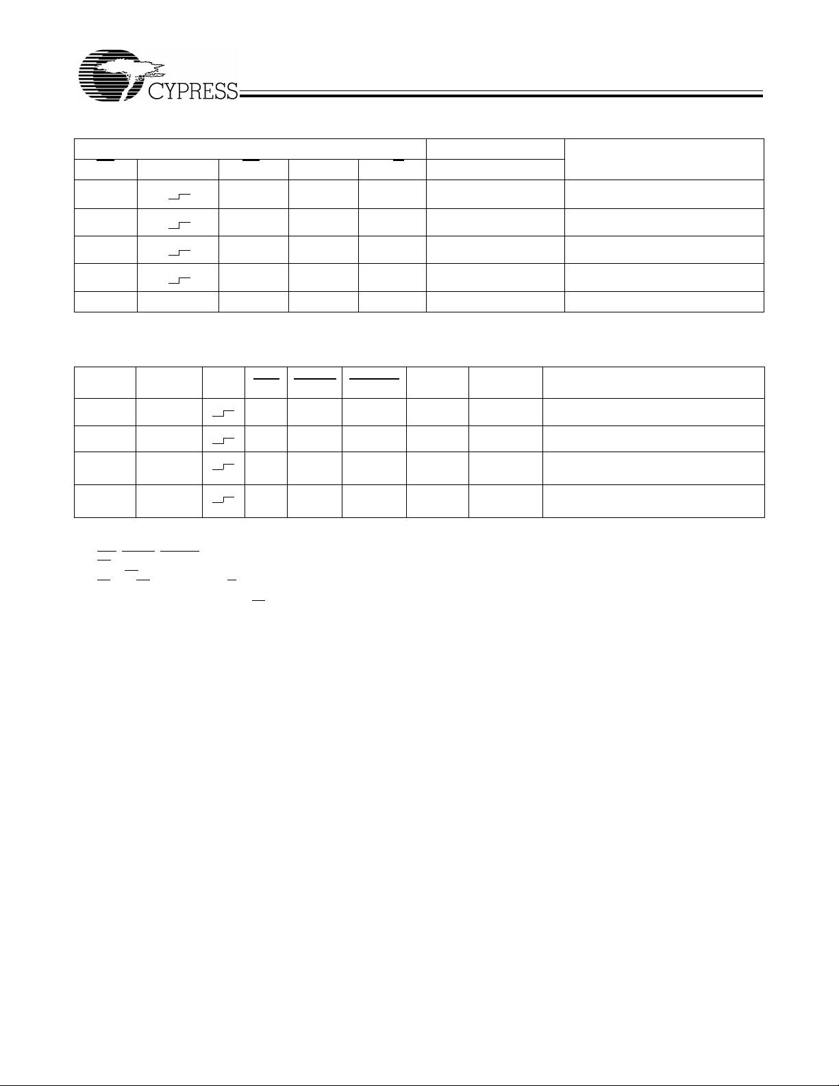
[24, 25, 26]
Inputs Outputs
OE CLK CE
0
CE
1
R/W I/O
I/O
–
0
17
X H X X High-Z Deselected
X X L X High-Z Deselected
X L H L D
L L H H D
IN
OUT
Write
Read
H X L H X High-Z Outputs Disabl ed
Address Counter Control Operation
[24, 28, 29 , 30]
Previous
Address
X X X X L D
A
X A
Address CLK ADS CNTEN CNTRST I/O Mode Operation
out(0)
n
X L X H D
n
H H H D
out(n)
out(n)
Reset Counter Reset to Address 0
Load Address Load into Counte r
Hold External Address Blocked—Counter
Disabled
X A
n
H L H D
out(n+1)
Increment Counter Enabled—Internal Address
Generation
Operation
[27]
[27]
[27]
Notes:
24. “X” = “Don’t Care,” “H” = V
, CNTEN, CNTRST = “Don’t Care.”
25. ADS
26. OE is an asynchronous input signal.
27. When CE changes state In the pipelined mode, deselection and read happen in the following clock cycle.
28. CE0 and OE = VIL; CE1 and R/W = VIH.
29. Data shown for flow-through mode; pipelined mode output will be delayed by one cycle.
30. Counter operation is independent of CE
, “L” = VIL.
IH
and CE1.
0
15

CY7C09349AV
CY7C09359AV
Ordering Information
4K x18 3.3V Synchronous Dual-Port SRAM
Speed
(ns) Ordering Code
9 CY7C09349AV–9AC A100 100-Pin Thin Quad Flat Pack Commercial
12 CY7C09349AV–12AC A100 100-Pin Thin Quad Flat Pack Commercial
8K x18 3.3V Synchronous Dual-Port SRAM
Speed
(ns)
Ordering Code
9 CY7C09359AV–9AC A100 100-Pin Thin Quad Flat Pack Commercial
12 CY7C09359AV–12AC A100 100-Pin Thin Quad Flat Pack Commercial
CY7C09359AV–12AI A100 100-Pin Thin Quad Flat Pack Industrial
Document #: 38—00840-A
Package Diagram
100-Pin Thin Plastic Quad Fl at Pack (T QF P) A100
Package
Name Package Type
Package
Name
Package Type
Operating
Range
Operating
Range
51-85048-B
© Cypress Semiconductor Corporation, 2000. The information contained herein is subject to change without notice. Cypress Semiconductor Corporation assumes no responsibility for the use
of any circuitry other than circuitry embodied in a Cypress Semiconductor product. Nor does it conv ey or imply any lice nse under patent or other rights. Cypress Semicondu ctor does not authorize
its products for use as critical components in life-support systems where a malfunction or failure may reasonably be expected to result in significant injury to the user. The inclusion of Cypress
Semiconductor products in life-support systems application implies that the manufacturer assumes all risk of such use and in doing so indemnifies Cypress Semiconductor against all charges.
 Loading...