

1
查询CY7C91079V供应商
CY7C09079V/89V/99V
PRELIMINARY
Features
• T rue Dual-P orted memory cell s which allow simultaneous access of the same memory location
• 6 Flow-Through/Pipelined devices
—32K x 8/9 organizations (CY7C09079V/179V)
—64K x 8/9 organizations (CY7C09089V/189V)
—128K x 8/9 organizations (CY7C09099V/199V)
• 3 Modes
—Flow-Through
—Pipelined
—Burst
• Pipelined output mode on both ports allows fast
100-MHz operation
• 0.35-micron CMOS for optimum speed/power
v
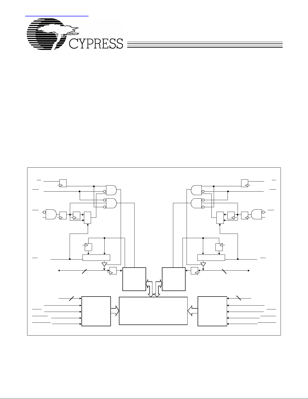
Logic Block Diagram
R/W
L
OE
L
CY7C09179V/89V/99V
3.3V 32K/64K/128K x 8/9
Synchronous Dual-Port Static RAM
• High-speed clock to data access 6.5
[1, 2]
(max.)
• 3.3V low operating power
—Active= 115 mA (typical)
— Standby= 10 µA (typ ical)
• Fully synchronous interfa ce for easier operatio n
• Burst coun ters increment addresses internally
—Shorten cycle times
—Minimize bus noise
—Supported in Flow-Through and Pip eli ned m odes
• Dual Chip Enables f or easy depth expansion
• Automatic power-down
• Commercial and Industrial temper ature ranges
Available in 100-pin TQFP
•
/7.5
[2]
/9/12 ns
R/W
OE
R
R
CE
0L
CE
1L
FT/Pipe
I/O0L–I/O
A
CLK
ADS
CNTEN
CNTRST
Notes:
1. Call for availability.
2. See page 6 for Load Conditions.
3. I/O
4. A
L
[3]
7/8L
[4]
0–A14/15/16L
L
L
L
–I/O7 for x8 devices; I/O0–I/O8 for x9 devices.
0
for 32K; A0–A15 for 64K; and A0–A16 for 128K devices.
0–A14
15/16/17
L
Counter/
Address
Register
Decode
1
0
0/1
1
0/1
1
0
0/1
1
0/1
8/9 8/9
0
I/O
Control
I/O
Control
0
Counter/
Address
Register
True Dual-Ported
RAM Array
Decode
15/16/17
CE
CE
FT/Pipe
I/O0R–I/O
[4]
A
0–A14/15/16R
CLK
ADS
CNTEN
CNTRST
0R
1R
R
[3]
7/8R
R
R
R
R
For the most recent information, visit the Cypress web sit e at www.cypress.com
Cypress Semiconductor Corporation
• 3901 North First Street • San Jose • CA 95134 • 408-943-2600
September 23, 1999
CY7C09079V/89V/99V
PRELIMINARY
Functional Description
The CY7C09079V/89V/99V and CY7C09179V/89V/99V are
high-speed synchronous CMOS 32K, 64K, and 128K x 8/9
dual-port static RAMs. Two ports are provided, permitting independent, simultaneous access for reads and writes to any
location in memory.
lines allow for m ini m al set-up and hold times. In pipelin ed output mode, data is registered for decreased cycle time. Clock
to data valid t
can also be used to bypass the pipelined output register to
eliminate access latency. In flow-through mode data will be
available t
CD1
device. Pipelined output or flow-through mode is selected via
the FT
/Pipe pin.
Each port contains a b urst co unter on t he input address register. The internal write pulse width is independent of the
LOW-to-HIGH transi tion of the clock signal. The internal write
pulse is self-t imed to allow the shortest possib le cycle times.
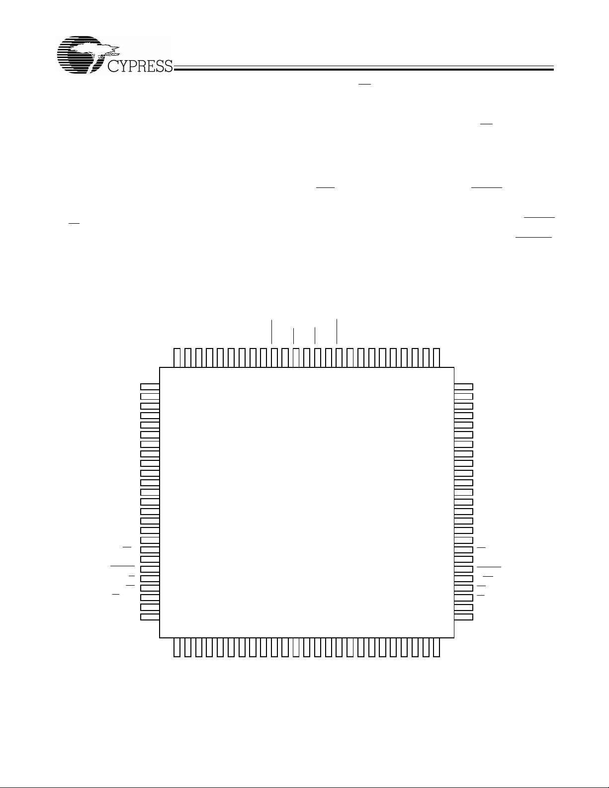
Pin Configurations
[5]
Registers on control, address , and data
CD2
= 6.5 ns
[1, 2]
(pipelined). Flow-thro ugh m ode
= 18 ns after the address is clocked into the
100-Pin TQFP
NCNCA6L
A5L
A4L
A3L
A1L
CNTENL
A0L
A2L
(Top View)
CY7C09179V/89V/99V
A HIGH on CE
down the in ternal ci rcuitry to r educe the static power consumption. The use of multiple Chip Enables allows easier banking
of multiple chips for depth expansion configurations. In the
pipelined mode, one cycle is requir ed with CE
HIGH to reactiv ate the outputs.
Counter enable inputs are pro vided to sta ll the oper ation of the
address input an d utilize the internal address gener ated b y the
internal counter for fast interleaved memory applications. A
port’s burst counter is loaded with the port’s Address Strobe
(ADS
). When the port’s Count Enable (CNTEN) is asserted,
the address counter will increment on each LOW-to-HIGH
transition of that port’s clock signal. This will read/write one
word from/in to each su cces siv e address locat io n until CNTEN
is deasserted. The counter can address the entire memory
array and will loop bac k to the start. Counter Reset (CNT RST
is used to reset the burst counter.
All parts are available in 100-pin Thin Quad Plastic Flatpack
(TQFP) packages.
CLKL
GND
ADSR
CLKR
ADSL
CNTENR
or LOW on CE1 for one clock cy cle will power
0
0
A0R
A1R
A2R
A3R
A4R
A5R
A6RNCNC
LOW and CE
1
)
CNTRSTL
[8]
FT
A10L
A11L
A12L
A13L
A14L
[6]
A15L
[7]
A16L
CE
CE1L
R/WL
/PIPEL
NC
NC
A7L
A8L
A9L
VCC
NC
NC
NC
NC
OE
NC
NC
92 91 90 848587 868889 83 82 81 7678 77798093949596979899100
1
2
3
4
5
6
7
8
9
10
11
12
13
14
15
16
0L
L
17
18
19
20
21
22
23
24
25
CY7C09099V (128K x 8)
CY7C09089V (64K x 8)
CY7C09079V (32K x 8)
34 35 36 424139 403837 43 44 45 5048 494746
3332313029282726
75
74
73
72
71
70
69
68
67
66
65
64
63
62
61
60
59
58
57
56
55
54
53
52
51
NC
NC
A7R
A8R
A9R
A10R
A11R
A12R
A13R
A14R
[6]
A15R
[7]
A16R
GND
NC
NC
NC
NC
0R
CE
CE1R
CNTRST
R/WR
OER
FT/PIPER
GND
NC
R
[8]
NC
GND
I/O7L
I/O4L
I/O5L
I/O6L
GND
I/O2L
I/O3L
VCC
GND
I/O0L
I/O1L
I/O0R
Notes:
5. When writing simultaneously to the same location, the final value cannot be guaranteed.
6. This pin is NC for CY7C09079V.
7. This pin is NC for CY7C09079V and CY7C09089V.
8. For CY7C09079V and CY7C09089V , pin #23 connected to V
compatible with an IDT 5V x16 flow-through device.
is pin compatible with an IDT 5V x8 pipelined device; connecting pin #23 and #53 to GND is pin
CC
2
I/01R
NC
NC
VCC
I/O2R
I/O5R
I/O3R
I/O4R
NC
I/O7R
I/O6R
CY7C09079V/89V/99V
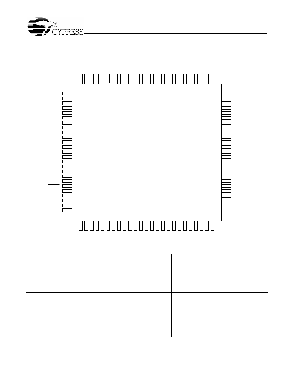
Pin Configurations
NC
NC
A7L
A8L
A9L
A10L
A11L
A12L
A13L
A14L
[9]
A15L
A16L
VCC
NC
NC
NC
NC
CE0L
CE1L
CNTRSTL
R/WL
OEL
FT/PIPEL
NC
NC
(continued)
NCNCA6L
1
2
3
4
5
6
7
8
9
10
11
12
13
14
15
16
17
18
19
20
21
22
23
24
25
PRELIMINARY
100-Pin TQFP
(Top View)
A5L
A4L
A3L
A1L
A2L
CLKL
CNTENL
A0L
92 91 90 848587 868889 83 82 81 7678 77798093949596979899100
GND
GND
ADSL
CY7C09199V (128K x 9)
CY7C09189V (64K x 9)
CY7C09179V (32K x 9)
34 35 36 424139 403837 43 44 45 5048 494746
3332313029282726
CY7C09179V/89V/99V
CNTENR
ADSR
A0R
CLKR
A1R
A2R
A3R
A4R
A5R
A6R
NC
75
74
73
72
71
70
69
68
67
66
65
64
63
62
61
60
59
58
57
56
55
54
53
52
51
NC
NC
A7R
A8R
A9R
A10R
A11R
A12R
A13R
A14R
[9]
A15R
[10][10]
A16R
GND
NC
NC
NC
NC
CE0R
CE1R
CNTRSTR
R/WR
OER
FT/PIPER
GND
NC
NC
VCC
GND
I/O7L
I/O8L
I/O4L
I/O5L
I/O6L
GND
I/O2L
I/O3L
I/O1L
GND
I/O0L
I/O0R
I/01R
VCC
I/O3R
I/O2R
I/O6R
I/O5R
I/O4R
NC
I/O8R
I/O7R
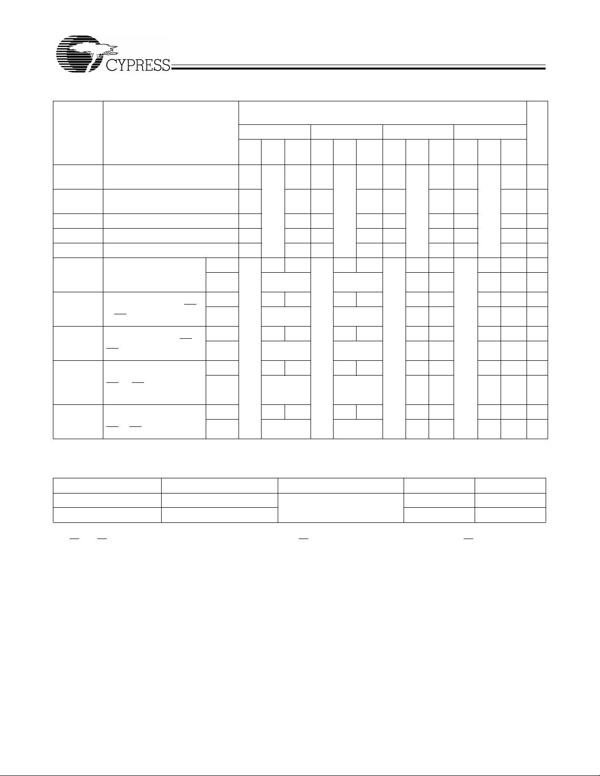
Selectio n Guide
CY7C09079V/89V/99V
CY7C09179V/89V/99V
f
(MHz) (Pipel ined) 100 83 67 50
MAX2
Max. Access Time (ns)
[1, 2]
-6
6.5 7.5 9 12
(Clock to Data,
Pipelined)
Typical Operating
Current I
CC
(mA)
T ypical Standby Curren t
for I
Port s TTL Level)
(mA) (Both
SB1
T ypical Standby Curren t
for I
(µA) (Both P orts
SB3
175 155 135 115
25 25 20 20
10 µA10 µA 10 µA10 µA
CMOS Level)
Notes:
9. This pin is NC for CY7C09179V.
10. This pin is NC for CY7C09179V and CY7C09189V.
CY7C09079V/89V/99V
CY7C09179V/89V/99V
[2]
-7
3
CY7C09079V/89V/99V
CY7C09179V/89V/99V
-9
CY7C09079V/89V/99V
CY7C09179V/89V/99V
-12
CY7C09079V/89V/99V
PRELIMINARY
Pin Definitions
Left Port Right Port Description
A0L–A
16L
ADS
L
CE0L,CE
CLK
L
CNTEN
CNTRST
I/O0L–I/O
OE
L
R/W
L
FT/PIPE
GND Ground Input.
NC No Connect.
V
CC
L
1L
L
8L
L
A0R–A
16R
ADS
R
CE0R,CE
CLK
R
CNTEN
CNTRST
I/O0R–I/O
OE
R
R/W
R
FT/PIPE
Address Inputs (A0–A14 for 32K; A0–A15 for 64K; and A0–A16 for 128K devices).
Address Strobe Input. Used as an address qualifier. This signal should be asserted LOW to
access the part using an e xternally supplied address. Asserting this signal LOW al so loads the
burst counter wit h the address present on the addr ess pins.
Chip Enable Input. To select either the l eft or right port, both CE0 AND CE1 must be asserted to
1R
their active states (CE
≤ VIL and CE1 ≥ VIH).
0
Clock Signal. This input can be free running or strobed. Ma ximum clock input rate is f
Counter Enable In put. Asserting this signal LO W increments the bur st address counter of its
R
respectiv e port on eac h rising ed ge of CLK. CNTEN
LOW.
Counter Reset I nput. Ass erting this si gnal LO W reset s the bu rst addre ss counter of its respecti ve
R
por t to zer o. CNTRS T
Data Bus Input/Output (I/O0–I/O7 for x8 de vices; I/O0–I/O8 for x9 de vices).
8R
is not disabled by asserting ADS or CNTEN.
Output Enable Input. This signal must be asserted LO W to enab le the I/O data pin s during read
operations.
Read/Write Enable I nput. This signal i s asserted LOW t o write to the dua l port memory array. For
read operation s, assert this pin HIGH.
Flow-Through/ Pipelined Sele ct Input. For flow -through mod e operatio n, assert this pin LOW. For
R
pipelined mode operation, assert this pin HIGH.
Power Input.
CY7C09179V/89V/99V
.
MAX
is disab led i f ADS or CNTRST are asse rted
Maximum Ratings
(Abov e which the useful life may be impaired. For user guidelines, not tested.)
Storage Temperature................ .. ............ ... –65
Ambient Temperature with Power Applied..–55
Supply Voltage to Ground Potential...............–0.5V to +4.6V
DC Voltage Applied to
Outputs in High Z State ...........................–0.5V to V
DC Input Voltage......................................–0.5V to V
°
C to +150°C
°
C to +125°C
+0.5V
CC
+0.5V
CC
Output Current into Outputs (LOW)............................. 20 mA
Static Discharge Voltage .......... ............ .....................>2001V
Latch -U p Cu rre n t....... ......... ... ......... ... .......... .. .......... . >200mA
Operating Range
Ambient
Range
Commercial 0°C to +70°C 3.3V ± 300 mV
Industrial –40
Temperature
°
C to +85°C 3.3V ± 300 mV
V
CC
4
CY7C09079V/89V/99V
Electrical Characteristics
Parameter Description
V
V
V
V
I
OZ
I
CC
I
SB1
I
SB2
I
SB3
I
SB4
OH
OL
IH
IL
Output HIGH Voltage (VCC=Min.,
I
= –4.0 mA)
OH
Output LOW Voltage (VCC=Min.,
I
= +4.0 mA)
OH
Input HIGH Voltage 2.0 2.0 2.0 2.0 V
Input LOW Voltage 0.8 0.8 0.8 0.8 V
Output Leakage Current –10 10 –10 10 –10 10 –10 10 µA
Operating Current
(V
=Max., I
CC
Outputs Disabled
Standby Current (Both
Ports TTL Level)
& CE
≥ VIH, f=f
R
Standby Current (One
Port TTL Level)
CE
≥ VIH, f=f
R
OUT
[11]
MAX
=0 mA)
[11]
MAX
Standby Current (Both
Ports CMOS Level)
CEL & CER ≥ VCC – 0.2V,
f=0
Standby Current (One
Port CMOS Level)
[11]
CEL | CER ≥ VIH, f=f
PRELIMINARY
CY7C09179V/89V/99V
Over the Operating Range
CY7C09079V/89V/99V
CY7C09179V/89V/99V
[1, 2]
-6
Min.
Typ.
Max.
[2]
-7
Min.
Typ.
Max.
-9 -12
Min.
Typ.
Max.
Min.
2.42.42.42.4 V
0.4 0.4 0.4 0.4 V
Com’l. 175 320 155 275 135 225 115 205 mA
Indust. 185 295 mA
Com’l. 25 95 25 85 20 65 20 50 mA
CEL
Indust. 35 75 mA
Com’l. 115 175 105 165 95 150 85 140 mA
CEL |
Indust. 105 160 mA
Com’l. 10 250 10 250 10 250 10 250 µA
[11]
Indust. 10 250 µA
Com’l. 105 135 95 125 85 115 75 100 mA
Indust. 95 125 mA
MAX
Typ.
Max.
Units
Capacitance
Parameter Description Te st Condi tions Max. Unit
C
IN
C
OUT
Note:
11. CE
and CER are internal signals. To select either the left or right port, both CE0 AND CE1 must be asserted to their active states (CE0 ≤ VIL and CE1 ≥ VIH).
L
Input Capacitance TA = 25°C, f = 1 MHz,
V
= 3.3V
Output Capacitance 10 pF
CC
10 pF
5
CY7C09079V/89V/99V
PRELIMINARY
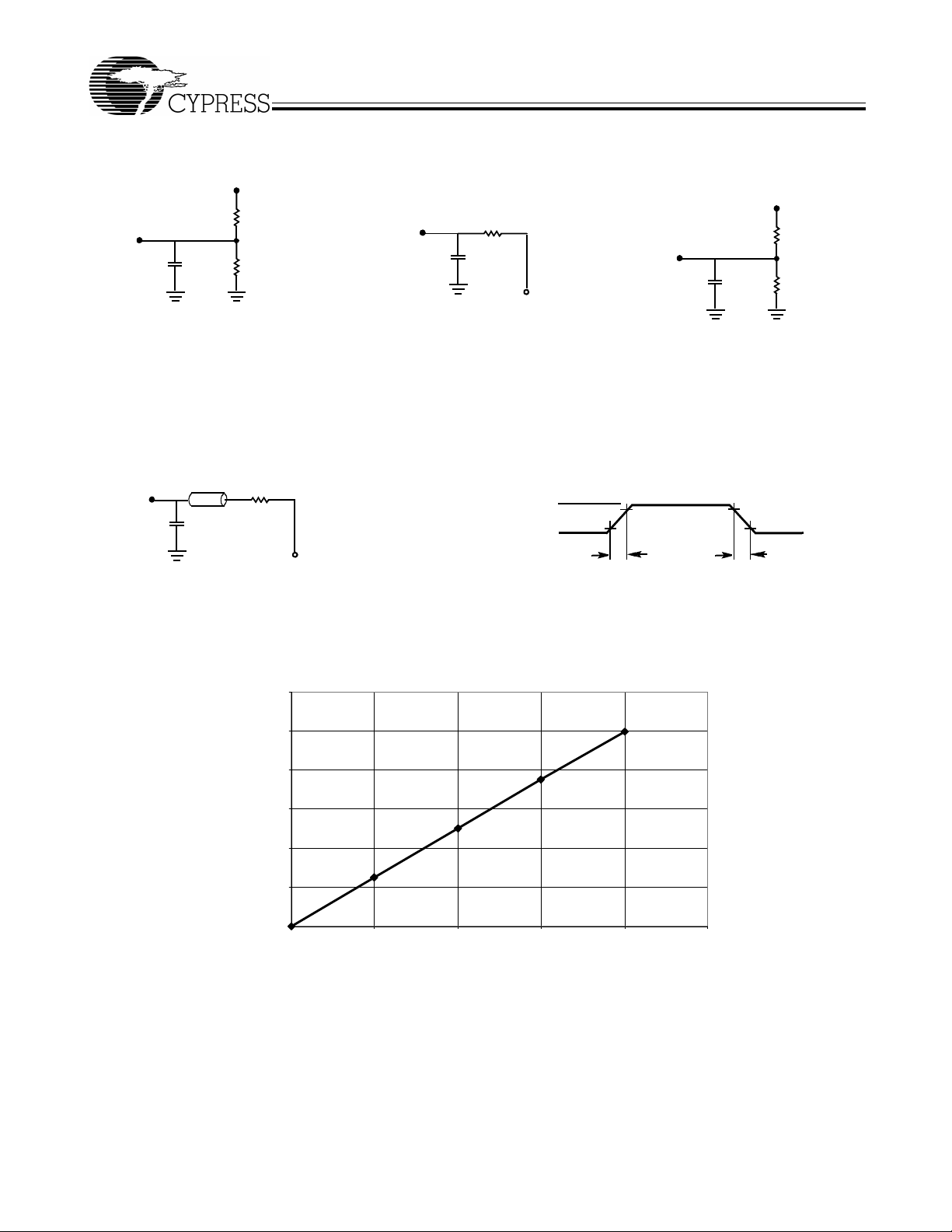
AC Test Loads
3.3V
R1= 590
OUTPUT
pF
C= 30
R2= 435
(a) Normal Load(Load 1)
AC Test Loads (Applicable to -6 and -7 only)
Z0 = 50
Ω
OUTPUT
C
R = 50
Ω
Ω
Ω
VTH=1.4V
OUTPUT
C=
30 pF
(b) Thévenin Equivalent (Load 1)
[12]
R
TH
=250
Ω
3.0V
GND
V
TH
≤
=1.4V
10%
3ns
CY7C09179V/89V/99V
3.3V
R1= 590
OUTPUT
C= 5pF
(c)Three-State Delay(Load 2)
(Used for t
CKLZ
including scope and jig)
ALL INPUTPULSES
90%
90%
, t
OLZ
10%
R2= 435
, & t
3
ns
≤
Ω
Ω
OHZ
(a) Load 1 (-6 and -7 only)
(ns) for al l -7 access times
∆
0.60
0.50
0.40
0.30
0.20
0.1 0
0.00
1 0 1 5 20 25 30 35
Capacitance (pF)
(b) Load Derating Curve
Note:
12. Test Conditions: C = 10 pF.
6

CY7C09079V/89V/99V
PRELIMINARY
Switching Characteristics
Parameter Description
f
MAX1
f
MAX2
t
CYC1
t
CYC2
t
CH1
t
CL1
t
CH2
t
CL2
t
R
t
F
t
SA
t
HA
t
SC
t
HC
t
SW
t
HW
t
SD
t
HD
t
SAD
t
HAD
t
SCN
t
HCN
t
SRST
t
HRST
t
OE
[13,14]
t
OLZ
[13,14]
t
OHZ
t
CD1
t
CD2
t
DC
[13,14]
t
CKHZ
[13,14]
t
CKLZ
Port to Port Delays
t
CWDD
t
CCS
Notes:
13. Test conditions used are Load 2.
14. This parameter is guaranteed by design, but it is not production tested.
f
Flow-Through 53 45 40 33 MHz
Max
f
Pipelined 100 83 67 50 MHz
Max
Clock Cycle Ti m e - Flo w -Through 19 22 25 30 ns
Clock Cycle Ti me - Pipelined 10 12 15 20 ns
Clock HIGH Time - Flow -Through 6 .5 7.5 12 12 ns
Clock LOW Time - Flow-Through 6.5 7.5 12 12 ns
Clock HIGH Time - Pipeli ned 4 5 6 8 ns
Clock LOW Time - Pi pelined 4 5 6 8 ns
Clock Rise Time 3 3 3 3 ns
Clock Fall Time 3 3 3 3 ns
Addr ess Set-Up Time 3. 5 4 4 4 ns
Address Hold Time 0 0 1 1 ns
Chip Enable Set-Up Time 3.5 4 4 4 ns
Chip Enable Hold Time 0 0 1 1 ns
R/W Set-Up Time 3.5 4 4 4 ns
R/W Hold Time 0 0 1 1 ns
Input Data Set-Up Time 3.5 4 4 4 ns
Input Data Hold Time 0 0 1 1 ns
ADS Set-Up Time 3.5 4 4 4 ns
ADS Hold Time 0 0 1 1 ns
CNTEN Set-Up Time 3.5 4.5 5 5 ns
CNTEN Hold Time 0 0 1 1 ns
CNTRST Set-Up Time 3.5 4 4 4 ns
CNTRST Hold Time 0 0 1 1 ns
Output Enable to Data Valid 8 9 10 12 ns
OE to Low Z 2 2 2 2 ns
OE to High Z 17171717ns
Clock to Data Valid - Flow-Through 15 18 20 25 ns
Clock to Data Valid - Pipelined 6.5 7.5 9 12 ns
Data Output Hold After Clock HIGH 2 2 2 2 ns
Clock HIGH to Output High Z 29292929ns
Clock HIGH to Output Low Z 2 2 2 2 ns
Write Port Cloc k HIGH to Read Data Dela y 30 35 40 40 ns
Clock to Clock Set-Up Time 9 10 15 15 ns
Over the Operating Range
-6
[1, 2]
Min.
CY7C09079V/89V/99V
CY7C09179V/89V/99V
[2]
-7
Min.
Max.
Max.
CY7C09179V/89V/99V
-9 -12
Min.
Max.
Min.
Max.
Units
7

CY7C09079V/89V/99V
PRELIMINARY
Switching Waveforms
Read Cycle for Flow-Through Output (FT
CLK
CE
0
t
SC
CE
1
R/W
ADDRESS
DATA
OUT
Read Cycle for Pipelined Operation (FT/PIPE = VIH)
CLK
OE
t
t
SW
SA
(continued )
t
CH1
t
HC
t
HW
t
HA
A
n
t
CKLZ
t
CH2
t
CD1
t
CYC2
t
CYC1
/PIPE = VIL)
t
CL1
A
n+1
t
CL2
[15, 16, 17, 18]
t
DC
Q
n
[15, 16, 17, 18]
CY7C09179V/89V/99V
t
SC
A
n+2
Q
n+1
t
OHZ
t
OLZ
t
OE
t
HC
A
n+3
t
CKHZ
Q
n+2
t
DC
CE
0
CE
t
SC
1
t
HC
R/W
ADDRESS
DATA
OUT
t
SW
t
SA
t
HW
t
HA
A
n
1 Latency
t
CKLZ
A
n+1
t
CD2
OE
Notes:
15. OE
is asynchronously controlled; all other inputs are synchronous to the rising clock edge.
= VIL, CNTEN and CNTRST = VIH.
16. ADS
17. The output is disabled (high-impedance state) by CE
18. Addresses do not have to be accessed sequentially since ADS
or CE1 = VIL following the next rising edge of the clock.
0=VIH
= VIL constantly loads the address on the rising edge of the CLK. Numbers are for reference only.
t
SC
A
n+2
t
DC
Q
n
Q
n+1
t
OHZ
t
HC
A
n+3
Q
n+2
t
OLZ
t
OE
8

CY7C09079V/89V/99V
PRELIMINARY
Switching Waveforms
Bank Select Pipelined Read
-
CLK
L
t
SA
ADDRESS
DATA
ADDRESS
DATA
Left Port Write to Flow-Through Right Port Read
(B1)
CE
0(B1)
OUT(B1)
(B2)
CE
0(B2)
OUT(B2)
t
SC
t
SA
t
SC
(continued )
[19, 20]
t
CH2
A
0
A
0
t
CYC2
t
HA
t
HC
t
HA
t
HC
t
CL2
A
1
t
CD2
A
1
A
2
t
SC
D
0
t
A
2
t
SC
[21, 22, 23, 24]
t
DC
HC
CY7C09179V/89V/99V
A
3
t
CD2
t
HC
t
CKHZ
D
1
t
DC
A
3
t
CD2
t
CKLZ
A
4
t
CD2
t
CKLZ
A
4
t
CKHZ
D
2
A
5
t
CKHZ
D
3
A
5
t
CD2
D
4
t
CKLZ
CLK
L
R/W
L
ADDRESS
ADDRESS
DATA
Notes:
19. In this depth expansion example, B1 represents Bank #1 and B2 is Bank #2; Each Bank consists of one Cypress dual-port device from this datasheet.
ADDRESS
20. OE
21. The same waveforms apply for a right port write to flow-through left port read.
22. CE
23. OE
24. It t
until t
L
DATA
INL
CLK
R
R/W
R
R
OUTR
(B1)
and ADS = VIL; CE
and ADS = VIL; CE1, CNTEN, and CNTRST = VIH.
0
= VIL for the right port, which is being read from. OE = VIH for the left port, which is being written to.
≤ maximum specified, then data from right port READ is not valid until the maximum specified for t
CCS
+ t
CCS
CD1
t
SW
t
SA
t
SD
= ADDRESS
. t
CWDD
(B2)
, CE
1(B1)
does not apply in this case.
MATCH
VALID
.
1(B2)
t
HW
t
HA
t
HD
t
CCS
t
CD1
t
SWtHW
t
SAtHA
MATCH
t
CWDD
t
DC
, R/W, CNTEN, and CNTRST = VIH.
NO
MATCH
NO
MATCH
t
CD1
VALID VALID
t
DC
. If t
CWDD
>maximum specified, then data is not valid
CCS
9

CY7C09079V/89V/99V
PRELIMINARY
t
A
n
(continued )
t
CYC2
CH2
t
HC
t
HW
t
HA
t
CL2
A
n+1
t
CD2
Switching Waveforms
Pipelined Read-to-Write-to-Read (OE = VIL)
CLK
CE
0
t
SC
CE
1
R/W
t
SW
ADDRESS
t
SA
DATA
IN
DATA
OUT
[18, 25, 26 , 27]
t
SW
Q
n
CY7C09179V/89V/99V
t
HW
A
n+2
t
CKHZ
A
n+2
tSDt
D
n+2
HD
A
n+3
t
CKLZ
A
n+4
t
CD2
Q
n+3
Pipelined Read-to-Write-to-Read (OE Controlled)
t
CYC2
t
t
t
HC
HW
HA
t
CL2
A
n+1
t
CD2
Q
t
OHZ
CLK
CE
CE
R/W
ADDRESS
DATA
DATA
OUT
t
CH2
0
t
SC
1
t
SW
A
n
t
SA
IN
[18, 25, 26, 27 ]
t
t
HW
SW
A
n+2
tSDt
D
n+2
n
NO OPERATION WRITEREAD READ
HD
A
n+3
D
n+3
A
n+4
t
CKLZ
A
n+5
t
CD2
Q
n+4
OE
READ READWRITE
Notes:
25. Output state (HIGH, LOW, or high-impedance) is determined by the previous cycle control signals.
26. CE
and ADS = VIL; CE1, CNTEN, and CNTRST = VIH.
0
27. During “No Operation”, data in memory at the selected address may be corrupted and should be re-written to ensure data integrity.
10

CY7C09079V/89V/99V
PRELIMINARY
t
CH1
A
n
t
CD1
t
CH1
(continued )
t
CYC1
t
CL1
t
HC
t
HW
t
HA
Q
n
t
t
CYC1
t
CL1
DC
A
n+1
t
READ
[16, 18, 25, 26, 27]
CD1
t
CKHZ
Switching Waveforms
Flow-Through Read-to-Write- to- R ead (OE = VIL)
CLK
CE
0
t
SC
CE
1
R/W
t
SW
ADDRESS
t
SA
DATA
IN
DATA
OUT
Flow-Through Read-to-Write- to- R ead (OE Controlled)
A
n+2
Q
n+1
NO
OPERATION
[16, 19, 25, 26, 27]
t
t
SW
SD
CY7C09179V/89V/99V
t
HW
A
n+2
t
D
n+2
WRITE READ
HD
A
n+3
t
CD1
t
CKLZ
A
n+4
t
CD1
Q
n+3
t
DC
CLK
CE
CE
R/W
ADDRESS
DATA
DATA
OUT
OE
0
t
SC
1
t
SW
A
t
SA
IN
t
HC
t
SW
t
HW
n
t
HA
t
CD1
A
n+1
t
t
DC
Q
n
SD
t
OHZ
A
n+2
D
n+2
READ
t
HW
A
n+3
t
HD
D
n+3
A
n+4
t
WRITE READ
OE
t
t
CKLZ
CD1
A
n+5
t
CD1
Q
n+4
t
DC
11

CY7C09079V/89V/99V
PRELIMINARY
t
CYC2
t
CH2
t
n
t
HAD
t
HCN
READ
EXTERNAL
ADDRESS
(continued )
t
CL2
HA
Q
t
CD2
x
t
DC
READ WITH COUNTER
Switching Waveforms
Pipelined Read with Address Counter Advance
CLK
t
SA
ADDRESS
ADS
CNTEN
DATA
OUT
t
SAD
t
SCN
A
Q
x-1
[28]
CY7C09179V/89V/99V
t
SAD
t
SCN
Q
n
Q
t
HAD
t
HCN
n+1
COUNTER HOLD
Q
n+2
READ WITH COUNTER
Q
n+3
Flow-Through Read with Address Counter Advance
t
CYC1
ADDRESS
CNTEN
DATA
Note:
28. CE
t
CH1
CLK
t
SA
A
n
t
SAD
ADS
t
SCN
OUT
Q
x
t
DC
EXTERNAL
ADDRESS
and OE = VIL; CE1, R/W and CNTRST = VIH.
0
t
t
HAD
t
HCN
t
CD1
READ
HA
t
CL1
Q
n
READ WITH COUNTER
[28]
t
SAD
t
SCN
Q
n+1
Q
n+2
COUN TER HOLD
t
HAD
t
HCN
READ
WITH
Q
n+3
COUNTER
12

CY7C09079V/89V/99V
PRELIMINARY
t
CH2
A
n
D
n
ADDRESS
(continued )
t
CYC2
t
CL2
t
HA
A
n
t
HAD
t
HCN
t
HD
D
n+1
WRIT E WITH
COUNTER
A
n+1
D
n+1
WRITE COUNTER
HOLD
D
n+2
Switching Waveforms
Write with Address Counter Advance (Flow-Through or Pipelined Outputs)
CLK
t
SA
ADDRESS
INTERNAL
ADDRESS
t
SAD
ADS
CNTEN
t
SCN
DATA
IN
t
SD
WRITE EXTERNAL
[29, 30]
CY7C09179V/89V/99V
A
n+2
D
n+3
WRITE WITH COUNTER
A
n+3
D
n+4
A
n+4
Notes:
29. CE
and R/W = VIL; CE1 and CNTRST = VIH.
0
30. The “Internal Addres s” is equal to the “External Address” when ADS
= VIL and equals the counter output when ADS = VIH.
13

CY7C09079V/89V/99V
Switching Waveforms
(continued )
Counter Reset (Pi p e lined Outputs)
t
CYC2
CLK
ADDRESS
INTERNAL
ADDRESS
R/W
ADS
CNTEN
CNTRST
t
SAD
t
SCN
t
SRST
t
CH2
A
X
t
HAD
t
HCN
t
HRST
t
CL2
t
PRELIMINARY
[18, 25, 31, 32 ]
01A
SWtHW
tSDt
HD
CY7C09179V/89V/99V
t
SAtHA
A
n
A
n+1
n
A
n+1
DATA
IN
DATA
OUT
COUNTER
RESET
Notes:
= VIL; CE1 = VIH.
31. CE
0
32. No dead cycle exists during counter reset. A READ or WRITE cycle may be coincidental with the counter reset.
D
0
WRITE
ADDRESS 0
READ
ADDRESS 0
READ
ADDRESS 1
Q
0
READ
ADDRESS n
Q
1
Q
n
14

CY7C09079V/89V/99V
PRELIMINARY
Read/W rite and Enable Operation
[33, 34, 35]
CY7C09179V/89V/99V
Inputs Outputs
OE CLK CE
0
CE
1
R/W I/O
I/O
–
0
9
X H X X High-Z Deselected
X X L X High-Z Deselected
X L H L D
L L H H D
IN
OUT
Write
Read
H X L H X High-Z Outputs Disabl ed
Address Counter Control Operation
[33, 37, 38, 39]
Previous
Address
X X X X L D
A
X A
Address
n
X L X H D
CLK ADS CNTEN CNTRST I/O Mode Operation
out(0)
out(n)
n
H H H D
out(n)
Reset Counter Reset to Address 0
Load Address Load into Counte r
Hold External Address Bloc ked—Counter
Disabled
X A
n
H L H D
out(n+1)
Increment Counter Enabled—Internal Address
Generation
Operation
[36]
[36]
[36]
Notes:
33. “X” = “don’t care”, “H” = V
, CNTEN, CNTRST = “don’t care”.
34. ADS
35. OE is an asynchronous input signal.
36. When CE changes state in the pipelined mode, deselection and read happen in the following clock cycle.
37. CE0 and OE = VIL; CE1 and R/W = VIH.
38. Data shown for flow-through mode; pipelined mode output will be delayed by one cycle.
39. Counter operation is independent of CE
, “L” = VIL.
IH
and CE1.
0
15

CY7C09079V/89V/99V
PRELIMINARY
CY7C09179V/89V/99V
Ordering Information
32K x8 3.3V Synchronous Dual -Port SRAM
Speed (ns) Ordering Code Package Name Pack ag e Type OperatingRange
[1, 2]
6.5
[2]
7.5
9 CY7C09079V-9AC A100 100-Pin Thin Quad Flat Pack Commercial
12 CY7C09079V-12AC A100 100-Pin Thin Quad Flat Pack Commercial
64K x8 3.3V Synchronous Dual -Port SRAM
Speed (ns) Ordering Code Package Name Package Type Operating Range
[1, 2]
6.5
[2]
7.5
9 CY7C09089V-9AC A100 100-Pin Thin Quad Flat Pac k Commercial
12 CY7C09089V-12AC A100 100-Pin Thin Quad Flat Pack Commercial
128K x8 3.3V Synchronous Dual-Port SRAM
Speed (ns) Ordering Code Package Name Package Type Operating Range
6.5
7.5
12 CY7C09099V-12AC A100 100-Pin Thin Quad Flat Pack Commercial
CY7C09079V-6AC A100 100-Pin Thin Quad Flat Pack Commercial
CY7C09079V-7AC A100 100-Pin Thin Quad Flat Pack Commercial
CY7C09079V-9AI A100 100-Pin Thin Quad Flat Pack Industrial
CY7C09089V-6AC A100 100-Pin Thin Quad Flat Pack Commercial
CY7C09089V-7AC A100 100-Pin Thin Quad Flat Pack Commercial
CY7C09089V-9AI A100 100-Pin Thin Quad Flat P ack Industrial
[1, 2]
[2]
CY7C09099V- 6AC A100 100-Pin Thin Quad Flat Pack Commercial
CY7C09099V- 7AC A100 100-Pin Thin Quad Flat Pack Commercial
9 CY7C09099V-9AC A100 100-Pin Thin Quad Flat Pack Commercial
CY7C09099V- 9AI A100 100-Pin Thin Quad Flat Pack Industrial
32K x9 3.3V Synchronous Dual -Port SRAM
Speed (ns) Ordering Code Package Name Pac kage Type Operating Range
6.5
7.5
[1, 2]
[2]
CY7C09179V- 6AC A100 100-Pin Thin Quad Flat Pack Commercial
CY7C09179V- 7AC A100 100-Pin Thin Quad Flat Pack Commercial
9 CY7C09179V-9C A100 100-Pin Thin Quad Flat Pack Commercial
CY7C09179V- 9AI A100 100-Pin Thin Quad Flat Pack Industrial
12 CY7C09179V-12AC A100 100-Pin Thin Quad Flat Pack Commercial
64K x9 3.3V Synchronous Dual -Port SRAM
Speed (ns) Ordering Code Package Name Package Type Operating Range
6.5
7.5
[1, 2]
[2]
CY7C09189V-6AC A100 100-Pin Thin Quad Flat P ack Commercial
CY7C09189V-7AC A100 100-Pin Thin Quad Flat P ack Commercial
9 CY7C09189V-9AC A100 100-Pin Thin Quad Flat Pack Commercial
CY7C09189V-9AI A100 100-Pin Thin Q uad Flat Pack Industrial
12 CY7C09189V- 12AC A100 100-Pin Thin Q uad Flat Pack Commercial
128K x9 3.3V Synchronous Dual-Port SRAM
Speed (ns) Ordering Code Package Name Package Type Operating Range
6.5
7.5
[1, 2]
[2]
CY7C09199V-6AC A100 100-Pin Thin Quad Flat Pack Commercial
CY7C09199V-7AC A100 100-Pin Thin Quad Flat Pack Commercial
9 CY7C09199V-9A C A100 100-Pin Thin Quad Flat Pack Commercial
CY7C09199V-9AI A100 100-Pin Thin Quad Flat Pack Industrial
12 CY7C09199V-12AC A100 100-Pin Thin Quad Flat Pac k Commercial
Document #: 38–00667–E
16

Package Diagram
PRELIMINARY
100-Pin Thin Plastic Quad Fl at Pack (T QF P) A100
CY7C09079V/89V/99V
CY7C09179V/89V/99V
51-85048-B
© Cypress Semiconductor Corporation, 1999. The information contained herein is subject to change without notice. Cypress Semiconductor Corporation assumes no responsibility for the use
of any circuitry other than circuitry embodied in a Cypress Semiconductor product. Nor does it con vey or imply any lice nse under patent or other rights. Cypress Semicondu ctor does not authorize
its products for use as critical components in life-support systems where a malfunction or failure may reasonably be expected to result in significant injury to the user. The inclusion of Cypress
Semiconductor products in life-support systems application implies that the manufacturer assumes all risk of such use and in doing so indemnifies Cypress Semiconductor against all charges.
 Loading...