

Page 1
FLEx36™ 3.3V 32K/64K/128K/256K x 36
Synchronous Dual-Port RAM
CY7C0850AV, CY7C0851AV
CY7C0852AV, CY7C0853AV
Features
Functional Description
■ True dual-ported memory cells that allow simultaneous access
of the same memory location
■ Synchronous pipelined operation
■ Organization of 1-Mbit, 2-Mbit, 4-Mbit, and 9-Mbit devices
■ Pipelined output mode allows fast operation
■ 0.18-micron CMOS for optimum speed and power
■ High-speed clock to data access
■ 3.3V low power
❐ Active as low as 225 mA (typ)
❐ Standby as low as 55 mA (typ)
■ Mailbox function for message passing
■ Global master reset
■ Separate byte enables on both ports
■ Commercial and industrial temperature ranges
■ IEEE 1149.1-compatible JTAG boundary scan
■ 172-Ball FBGA (1 mm pitch) (15 mm × 15 mm)
■ 176-Pin TQFP (24 mm × 24 mm × 1.4 mm)
■ Counter wrap around control
❐ Internal mask register controls counter wrap-around
❐ Counter-interrupt flags to indicate wrap-around
❐ Memory block retransmit operation
■ Counter readback on address lines
■ Mask register readback on address lines
■ Dual Chip Enables on both ports for easy depth expansion
The FLEx36™ family includes 1M, 2M, 4M, and 9M pipelined,
synchronous, true dual-port static RAMs that are high-speed,
low-power 3.3V CMOS. Two ports are provided, permitting
independent, simultaneous access to any location in memory.
The result of writing to the same location by more than one port
at the same time is undefined. Registers on control, address, and
data lines allow for minimal setup and hold time.
During a Read operation, data is registered for decreased cycle
time. Each port contains a burst counter on the input address
register. After externally loading the counter with the initial
address, the counter increments the address internally (more
details to follow). The internal Write pulse width is independent
of the duration of the R/W
input signal. The internal Write pulse
is self-timed to allow the shortest possible cycle times.
A HIGH on CE0
or LOW on CE1 for one clock cycle powers down
the internal circuitry to reduce the static power consumption. One
cycle with chip enables asserted is required to reactivate the
outputs.
Additional features include: readback of burst-counter internal
address value on address lines, counter-mask registers to
control the counter wrap-around, counter interrupt (CNTINT
flags, readback of mask register value on address lines,
retransmit functionality, interrupt flags for message passing,
JTAG for boundary scan, and asynchronous Master Reset
(MRST
).
The CY7C0853AV device in this family has limited features.
Please see See “Address Counter and Mask Register
Operations” on page 8. for details.
)
Table 1. Product Selection Guide
Density
1-Mbit
(32K x 36)
2-Mbit
(64K x 36)
4-Mbit
(128K x 36)
9-Mbit
(256K x 36)
Part Number CY7C0850AV CY7C0851AV CY7C0852AV CY7C0853AV
Max. Speed (MHz) 167 167 167 133
Max. Access Time - Clock to Data (ns) 4.0 4.0 4.0 4.7
Typical operating current (mA) 225 225 225 270
Package 176TQFP
172FBGA
176TQFP
172FBGA
176TQFP
172FBGA
172FBGA
Cypress Semiconductor Corporation • 198 Champion Court • San Jose, CA 95134-1709 • 408-943-2600
Document #: 38-06070 Rev. *H Revised July 29, 2008
[+] Feedback
Page 2
CY7C0850AV, CY7C0851AV
CY7C0852AV, CY7C0853AV
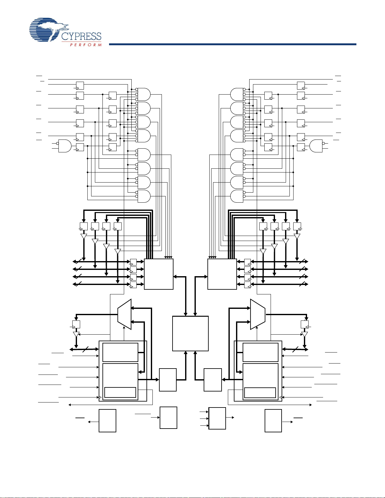
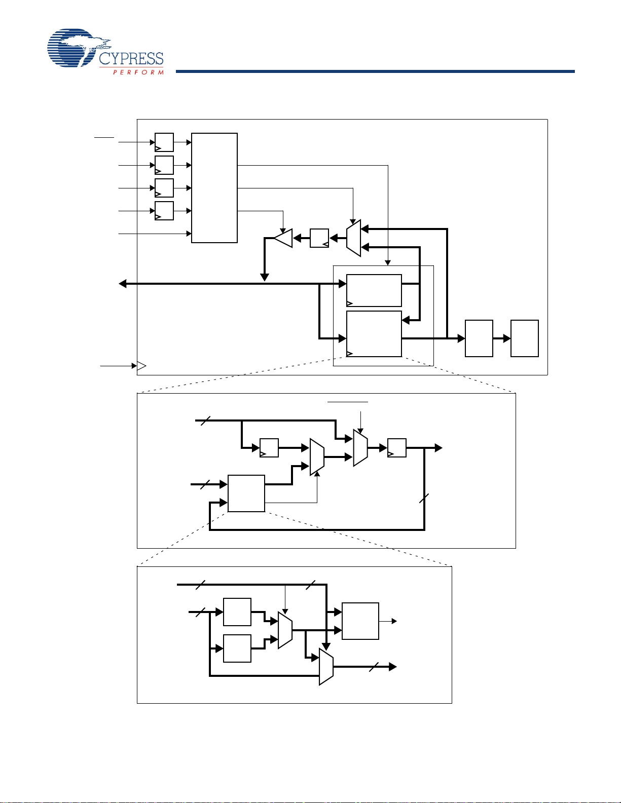
Logic Block Diagram
A0L–A
17L
CLK
L
ADS
L
CNTEN
L
CNTRST
L
True
RAM Array
18
Addr.
Read
Back
CNTINT
L
Mask Register
Counter/
Address
Register
CNT/MSK
L
Address
Decode
Dual-Ported
Interrupt
Logic
INT
L
Reset
Logic
JTAG
TDO
TMS
TCK
TDI
MRST
DQ9L–DQ
17L
DQ0L–DQ
8L
I/O
Control
9
9
9
9
DQ
18L
–DQ
26L
DQ
27L
–DQ
35L
CE
0L
CE
1L
R/W
L
B0
L
B1
L
B2
L
B3
L
OE
L
A0R–A
17R
CLK
R
ADS
CNTEN
CNTRST
R
18
Addr.
Read
Back
CNTINT
R
Mask Register
Counter/
Address
Register
CNT/MSK
R
Address
Decode
Interrupt
Logic
INT
R
DQ9R–DQ
17R
DQ0R–DQ
8R
I/O
Control
9
9
9
9
DQ
18R
–DQ
26R
DQ
27R
–DQ
35R
CE
0R
CE
1R
R/W
R
B0
R
B1
R
B2
R
B3
R
OE
R
Mirror Reg
Mirror Reg
Note
1. 9M device has 18 address bits, 4M device has 17 address bits, 2M device has 16 address bits, and 1M device has 15 address bits.
[1]
Document #: 38-06070 Rev. *H Page 2 of 32
[+] Feedback
Page 3
CY7C0850AV, CY7C0851AV
CY7C0852AV, CY7C0853AV
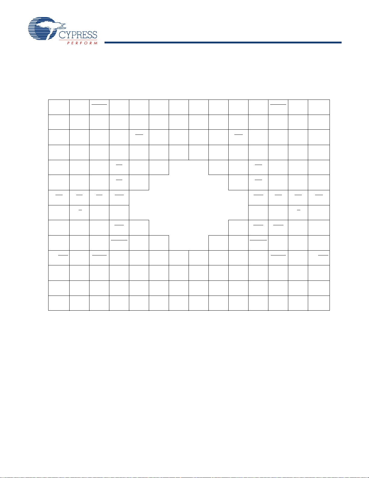
Pin Configurations
1234567891011121314
A
DQ32L DQ30L CNTINTL VSS DQ13L VDD DQ11L DQ11R VDD DQ13R VSS CNTINTR DQ30R DQ32R
B
A0L DQ33L DQ29L DQ17L DQ14L DQ12L DQ9L DQ9R DQ12R DQ14R DQ17R DQ29R DQ33R A0R
C
NC A1L DQ31L DQ27L INTL DQ15L DQ10L DQ10R DQ15R INTR DQ27R DQ31R A1R NC
D
A2L A3L DQ35L DQ34L DQ28L DQ16L VSS VSS DQ16R DQ28R DQ34R DQ35R A3R A2R
E
A4L A5L CE1L B0L VDD VSS VDD VDD B0R CE1R A5R A4R
F
VDD A6L A7L B1L VDD VSS B1R A7R A6R VDD
G
OEL B2L B3L CE0L
CY7C0850AV
CY7C0851AV
CY7C0852AV
CE0R B3R B2R OER
H
VSS R/WLA8LCLKL CLKR A8R R/WR VSS
J
A9L A10L VSS ADSL VSS VDD ADSR MRST A10R A9R
K
A11L A12L A15L
[2]
CNTRSTL VDD VDD VSS VDD CNTRSTR A15R
[2]
A12R A11R
L
CNT/MSKL A13L CNTENL DQ26L DQ25L DQ19L VSS VSS DQ19R DQ25R DQ26R CNTENR A13R CNT/MSKR
M
A16L
[2]
A14L DQ22L DQ18L TDI DQ7L DQ2L DQ2R DQ7R TCK DQ18R DQ22R A14R A16R
[2]
N
DQ24L DQ20L DQ8L DQ6L DQ5L DQ3L DQ0L DQ0R DQ3R DQ5R DQ6R DQ8R DQ20R DQ24R
P
DQ23L DQ21L TDO VSS DQ4L VDD DQ1L DQ1R VDD DQ4R VSS TMS DQ21R DQ23R
Note
2. For CY7C0851AV, pins M1 and M14 are NC. For CY7C0850AV, pins K3, K12 M1, and M14 are NC
Figure 1. 172-Ball BGA (Top View)
Document #: 38-06070 Rev. *H Page 3 of 32
[+] Feedback
Page 4

CY7C0850AV, CY7C0851AV
CY7C0852AV, CY7C0853AV
Pin Configurations (continued)
1234567891011121314
A
DQ32L DQ30L NC VSS DQ13L VDD DQ11L DQ11R VDD DQ13R VSS NC DQ30R DQ32R
B
A0L DQ33L DQ29L DQ17L DQ14L DQ12L DQ9L DQ9R DQ12R DQ14R DQ17R DQ29R DQ33R A0R
C
A17L A1L DQ31L DQ27L INTL DQ15L DQ10L DQ10R DQ15R INTR DQ27R DQ31R A1R A17R
D
A2L A3L DQ35L DQ34L DQ28L DQ16L VSS VSS DQ16R DQ28R DQ34R DQ35R A3R A2R
E
A4L A5L VDD B0L VDD VSS VDD VDD B0R VDD A5R A4R
F
VDD A6L A7L B1L VDD VSS B1R A7R A6R VDD
G
OEL B2L B3L VSS
CY7C0853AV
VSS B3R B2R OER
H
VSS R/WL A8L CLKL CLKR A8R R/WRVSS
J
A9L A10L VSS VSS VSS VDD VSS MRST A10R A9R
K
A11L A12L A15L VDD VDD VDD VSS VDD VDD A15R A12R A11R
L
VDD A13L VSS DQ26L DQ25L DQ19L VSS VSS DQ19R DQ25R DQ26R VSS A13R VDD
M
A16L A14L DQ22L DQ18L TDI DQ7L DQ2L DQ2R DQ7R TCK DQ18R DQ22R A14R A16R
N
DQ24L DQ20L DQ8L DQ6L DQ5L DQ3L DQ0L DQ0R DQ3R DQ5R DQ6R DQ8R DQ20R DQ24R
P
DQ23L DQ21L TDO VSS DQ4L VDD DQ1L DQ1R VDD DQ4R VSS TMS DQ21R DQ23R
Figure 2.
172-Ball BGA (Top View)
Document #: 38-06070 Rev. *H Page 4 of 32
[+] Feedback
Page 5
CY7C0850AV, CY7C0851AV
CY7C0852AV, CY7C0853AV
Pin Configurations (continued)
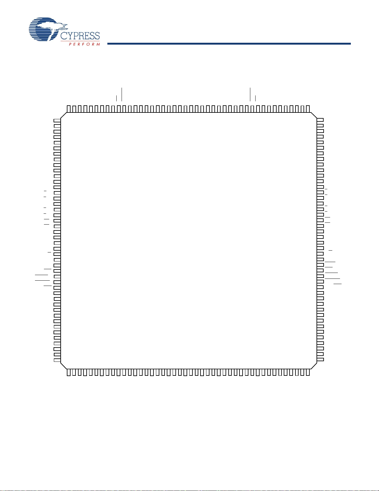
132
131
130
129
128
127
126
125
124
123
122
104
121
120
119
118
117
116
115
114
113
112
111
110
109
103
108
107
106
105
NC
A
6R
A
5R
A
4R
V
DD
V
SS
DQ
35R
DQ
34R
A
1R
A
2R
A
3R
A
0R
A
7R
B
0R
B
1R
CE
1R
B
2R
B
3R
OE
R
CE
0R
V
DD
V
DD
V
SS
V
SS
R/W
R
CLK
R
MRST
ADS
R
CNTEN
R
A
8R
CNTRST
R
CNT/MSK
R
A
9R
A
10R
A
11R
A
12R
V
SS
V
DD
A
13R
A
14R
A
15R
[2]
A
16R
[2]
DQ
24R
DQ
20R
NC
A
6L
A
5L
A
4L
V
DD
V
SS
DQ
35L
DQ
34L
A
1L
A
2L
A
3L
A
0L
A
7L
B
0L
B
1L
CE
1L
B
2L
B
3L
OE
L
CE
0L
V
DD
V
DD
V
SS
V
SS
R/W
L
CLK
L
V
SS
ADS
L
CNTEN
L
A
8L
CNTRST
L
CNT/MSK
L
A
9L
A
10L
A
11L
A
12L
V
SS
V
DD
A
13L
A
14L
A
15L
[2]
A
16L
[2]
DQ
24L
DQ
20L
DQ
33L
DQ
32L
DQ
31L
V
DD
V
SS
DQ
30L
DQ
28L
DQ
29L
DQ
27L
INT
L
CNTINT
L
DQ
16L
DQ
15L
DQ
17L
DQ
14L
DQ
13L
V
SS
V
DD
DQ
12L
DQ
11L
DQ
10L
DQ
9L
DQ
9R
DQ
10R
DQ
11R
DQ
12R
V
DD
V
SS
DQ
13R
DQ
14R
DQ
17R
DQ
15R
DQ
16R
CNTINT
R
INT
R
DQ
27R
DQ
29R
DQ
28R
DQ
30R
V
SS
V
DD
DQ
31R
DQ
32R
DQ
33R
DQ
26L
DQ
23L
DQ
22L
V
DD
V
SS
DQ
21L
DQ
25L
DQ
19L
DQ
18L
TDI
TDO
DQ
8L
DQ
7L
DQ
6L
DQ
5L
DQ
4L
V
SS
V
DD
DQ
3L
DQ
2L
DQ
1L
DQ
0L
DQ
0R
DQ
1R
DQ
2R
DQ
3R
V
DD
V
SS
DQ
4R
DQ
5R
DQ
6R
DQ
7R
DQ
8R
TMS
TCK
DQ
18R
DQ
19R
DQ
25R
DQ
21R
V
SS
V
DD
DQ
22R
DQ
23R
DQ
26R
102
91
101
100
99
98
97
96
90
95
94
93
92
89
1
2
3
4
5
6
7
8
9
10
11
29
12
13
14
15
16
17
18
19
20
21
22
23
24
30
25
26
27
28
31
42
32
33
34
35
36
37
43
38
39
40
41
44
176
175
174
173
172
171
170
169
168
167
166
165
164
163
162
161
160
159
158
157
156
155
154
153
152
151
150
149
148
147
146
145
144
143
142
141
140
139
138
137
136
135
134
133
45
46
47
48
49
50
51
52
53
54
55
56
57
58
59
60
61
62
63
64
65
66
67
68
69
70
71
727374
75
76
77
78
79
80
81
82
83
84
85
86
87
88
CY7C0850AV
CY7C0851AV
CY7C0852AV
Figure 3. 176-Pin Thin Quad Flat Pack (TQFP) (Top View)
Document #: 38-06070 Rev. *H Page 5 of 32
[+] Feedback
Page 6
CY7C0850AV, CY7C0851AV
CY7C0852AV, CY7C0853AV
Pin Definitions
Note
3. These pins are not available for CY7C0853AV device.
Left Port Right Port Description
A
0L–A17L
[3]
ADS
L
[3]
CE0
L
[3]
CE1
L
CLK
L
CNTEN
L
CNTRST
CNT/MSK
–DQ
DQ
0L
OE
L
[1]
[3]
[3]
L
L
35L
[3]
A0R–A
ADS
CE0
CE1
CLK
CNTEN
CNTRST
CNT/MSK
DQ0R–DQ
OE
INTLINTR Mailbox Interrupt Flag Output. The mailbox permits communications between ports. The upper
CNTINT
R/W
L
B
0L–B3L
[3]
L
CNTINT
R/W
B0R–B
MRST
TMS JTAG Test Mode Select Input. It controls the advance of JTAG TAP state machine. State
TDI JTAG Test Data Input. Data on the TDI input is shifted serially into selected registers.
TCK JTAG Test Clock Input.
TDO JTAG Test Data Output. TDO transitions occur on the falling edge of TCK. TDO is normally
V
SS
V
DD
[1]
17R
[3]
R
Address Inputs.
Address Strobe Input. Used as an address qualifier. This signal should be asserted LOW for
the part using the externally supplied address on the address pins and for loading this address
into the burst address counter.
[3]
R
[3]
R
R
[3]
R
Active LOW Chip Enable Input.
Active HIGH Chip Enable Input.
Clock Signal. Maximum clock input rate is f
MAX
.
Counter Enable Input. Asserting this signal LOW increments the burst address counter of its
respective port on each rising edge of CLK. The increment is disabled if ADS
or CNTRST are
asserted LOW.
[3]
R
R
Counter Reset Input. Asserting this signal LOW resets to zero the unmasked portion of the burst
address counter of its respective port. CNTRST
[3]
Address Counter Mask Register Enable Input. Asserting this signal LOW enables access to
is not disabled by asserting ADS or CNTEN.
the mask register. When tied HIGH, the mask register is not accessible and the address counter
operations are enabled based on the status of the counter control signals.
Data Bus Input/Output.
35R
R
Output Enable Input. This asynchronous signal must be asserted LOW to enable the DQ data
pins during Read operations.
two memory locations can be used for message passing. INT
port writes to the mailbox location of the left port, and vice versa. An interrupt to a port is
is asserted LOW when the right
L
deasserted HIGH when it reads the contents of its mailbox.
[3]
R
R
3R
Counter Interrupt Output. This pin is asserted LOW when the unmasked portion of the counter
is incremented to all “1s.”
Read/Write Enable Input. Assert this pin LOW to write to, or HIGH to Read from the dual port
memory array.
Byte Select Inputs. Asserting these signals enables Read and Write operations to the corresponding bytes of the memory array.
Master Reset Input. MRST is an asynchronous input signal and affects both ports. Asserting
MRST
LOW performs all of the reset functions as described in the text. A MRST operation is
required at power up.
machine transitions occur on the rising edge of TCK.
three-stated except when captured data is shifted out of the JTAG TAP.
Ground Inputs.
Power Inputs.
Document #: 38-06070 Rev. *H Page 6 of 32
[+] Feedback
Page 7
CY7C0850AV, CY7C0851AV
CY7C0852AV, CY7C0853AV
Master Reset
Notes
4. CE
is internal signal. CE = LOW if CE0 = LOW and CE1 = HIGH. For a single Read operation, CE only needs to be asserted once at the rising edge of the CLK and
can be deasserted after that. Data is out after the following CLK edge and is three-stated after the next CLK edge.
5. OE
is “Don’t Care” for mailbox operation.
6. At least one of B0
, B1, B2, or B3 must be LOW.
7. A16x is a NC for CY7C0851AV, therefore the Interrupt Addresses are FFFF and EFFF; A16x and A15x are NC for CY7C0850AV, therefore the Interrupt Addresses
are 7FFF and 6FFF.
8. “X” = “Don’t Care,” “H” = HIGH, “L” = LOW.
9. Counter operation and mask register operation is independent of chip enables.
The FLEx36 family devices undergo a complete reset by taking
its MRST
nously to the clocks. The MRST
counters to zero, and the counter mask registers to all ones
(completely unmasked). The MRST
Interrupt (INT
HIGH. The MRST
devices after power up.
input LOW. The MRST input can switch asynchro-
initializes the internal burst
also forces the Mailbox
) flags and the Counter Interrupt (CNTINT) flags
must be performed on the FLEx36 family
in order to set the INT
address 3FFFF asserts INT
active for a Write to generate an interrupt. A valid Read of the
3FFFF location by the right port resets INT
byte has to be active in order for a Read to reset the interrupt.
When one port Writes to the other port’s mailbox, the INT of the
port that the mailbox belongs to is asserted LOW. The INT
reset when the owner (port) of the mailbox Reads the contents
of the mailbox. The interrupt flag is set in a flow-thru mode (i.e.,
it follows the clock edge of the writing port). Also, the flag is reset
flag, a Write operation by the left port to
R
LOW. At least one byte has to be
R
HIGH. At least one
R
in a flow-thru mode (i.e., it follows the clock edge of the reading
Mailbox Interrupts
The upper two memory locations may be used for message
passing and permit communications between ports. Table 2
shows the interrupt operation for both ports of CY7C0853AV.
The highest memory location, 3FFFF is the mailbox for the right
port).
Each port can read the other port’s mailbox without resetting the
interrupt. And each port can write to its own mailbox without
setting the interrupt. If an application does not require message
passing, INT
pins should be left open.
port and 3FFFE is the mailbox for the left port. Ta bl e 2 shows that
L
[1, 4, 5, 6, 7]
CE
L
Left Port Right Port
A
0L–17L
INT
R/W
L
CE
R
R
A
0R–17R
INT
Table 2. Interrupt Operation Example
Function
R/W
Set Right INTR Flag L L 3FFFF X X X X L
Reset Right INTR Flag X X X X H L 3FFFF H
Set Left INTL Flag X X X L L L 3FFFE X
Reset Left INTL Flag H L 3FFFE H X X X X
is
R
Table 3. Address Counter and Counter-Mask Register Control Operation (Any Port)
[8, 9]
CLK MRST CNT/MSK CNTRST ADS CNTEN Operation Description
X L X X X X Master Reset Reset address counter to all 0s and mask
register to all 1s.
H H L X X Counter Reset Reset counter unmasked portion to all 0s.
H H H L L Counter Load Load counter with external address value
presented on address lines.
H H H L H Counter Readback Read out counter internal value on address
lines.
H H H H L Counter Increment Internally increment address counter value.
H H H H H Counter Hold Constantly hold the address value for
multiple clock cycles.
H L L X X Mask Reset Reset mask register to all 1s.
H L H L L Mask Load Load mask register with value presented on
the address lines.
H L H L H Mask Readback Read out mask register value on address
lines.
H L H H X Reserved Operation undefined
Document #: 38-06070 Rev. *H Page 7 of 32
[+] Feedback
Page 8

CY7C0850AV, CY7C0851AV
CY7C0852AV, CY7C0853AV
Address Counter and Mask Register
Notes
10. This section describes the CY7C0852AV, which have 17 address bits and a maximum address value of 1FFFF. The CY7C0851AV has 16 address bits, register lengths
of 16 bits, and a maximum address value of FFFF. The CY7C0850AV has 15 address bits, register lengths of 15 bits, and a maximum address value of 7FFF.
11. CNTINT
and CNTRST specs are guaranteed by design to operate properly at speed grade operating frequency when tied together.
Operations
This section
CY7C0850AV/CY7C0851AV/CY7C0852AV devices, but not to
the CY7C0853AV device. Each port of these devices has a
programmable burst address counter. The burst counter
contains three registers: a counter register, a mask register, and
a mirror register.
The counter register contains the address used to access the
RAM array. It is changed only by the Counter Load, Increment,
Counter Reset, and by master reset (MRST
The mask register value affects the Increment and Counter
Reset operations by preventing the corresponding bits of the
counter register from changing. It also affects the counter
interrupt output (CNTINT
the Mask Load and Mask Reset operations, and by the MRST
The mask register defines the counting range of the counter
register. It divides the counter register into two regions: zero or
more “0s” in the most significant bits define the masked region,
one or more “1s” in the least significant bits define the unmasked
region. Bit 0 may also be “0,” masking the least significant
counter bit and causing the counter to increment by two instead
of one.
The mirror register is used to reload the counter register on
increment operations (see “retransmit,” below). It always
contains the value last loaded into the counter register, and is
changed only by the Counter Load operation, and by the MRST
Table 3 on page 7 summarizes the operation of these registers
and the required input control signals. The MRST
is asynchronous. All the other control signals in Table 3 on page
7 (CNT/MSK, CNTRST, ADS, CNTEN) are synchronized to the
port’s CLK. All these counter and mask operations are
independent of the port’s chip enable inputs (CE0 and CE1).
Counter enable (CNTEN) inputs are provided to stall the
operation of the address input and utilize the internal address
generated by the internal counter for fast, interleaved memory
applications. A port’s burst counter is loaded when the port’s
address strobe (ADS
port’s CNTEN
address counter increments on each LOW to HIGH transition of
that port’s clock signal. This will Read/Write one word from/into
each successive address location until CNTEN
The counter can address the entire memory array, and loops
back to the start. Counter reset (CNTRST
unmasked portion of the burst counter to 0s. A counter-mask
register is used to control the counter wrap.
Counter Reset Operation
All unmasked bits of the counter are reset to “0.” All masked bits
remain unchanged. The mirror register is loaded with the value
of the burst counter. A Mask Reset followed by a Counter Reset
[10]
describes the features only apply to
) operations.
). The mask register is changed only by
control signal
) and CNTEN signals are LOW. When the
is asserted and the ADS is deasserted, the
is deasserted.
) is used to reset the
will reset the counter and mirror registers to 00000, as will master
reset (MRST
).
Counter Load Operation
The address counter and mirror registers are both loaded with
the address value presented at the address lines.
Counter Readback Operation
The internal value of the counter register can be read out on the
address lines. Readback is pipelined; the address is valid t
after the next rising edge of the port’s clock. If address readback
occurs while the port is enabled (CE0
data lines (DQs) is three-stated. Figure 4 on page 10 shows a
block diagram of the operation.
LOW and CE1 HIGH), the
Counter Increment Operation
Once the address counter register is initially loaded with an
.
external address, the counter can internally increment the
address value, potentially addressing the entire memory array.
Only the unmasked bits of the counter register are incremented.
The corresponding bit in the mask register must be a “1” for a
counter bit to change. The counter register is incremented by 1
if the least significant bit is unmasked, and by 2 if it is masked. If
all unmasked bits are “1,” the next increment wraps the counter
back to the initially loaded value. If an Increment results in all the
unmasked bits of the counter being “1s,” a counter interrupt flag
(CNTINT
register to its initial value, which was stored in the mirror register.
.
The counter address can instead be forced to loop to 00000 by
externally connecting CNTINT
results in one or more of the unmasked bits of the counter being
“0” deasserts the counter interrupt flag. The example in Figure 5
on page 11 shows the counter mask register loaded with a mask
value of 0003Fh unmasking the first 6 bits with bit “0” as the LSB
and bit “16” as the MSB. The maximum value the mask register
can be loaded with is 1FFFFh. Setting the mask register to this
value allows the counter to access the entire memory space. The
address counter is then loaded with an initial value of 8h. The
base address bits (in this case, the 6th address through the 16th
address) are loaded with an address value but do not increment
once the counter is configured for increment operation. The
counter address starts at address 8h. The counter increments its
internal address value till it reaches the mask register value of
3Fh. The counter wraps around the memory block to location 8h
at the next count. CNTINT
its maximum value.
) is asserted. The next Increment returns the counter
to CNTRST.
is issued when the counter reaches
[11]
An increment that
Counter Hold Operation
The value of all three registers can be constantly maintained
unchanged for an unlimited number of clock cycles. Such
operation is useful in applications where wait states are needed,
or when address is available a few cycles ahead of data in a
shared bus interface.
CA2
Document #: 38-06070 Rev. *H Page 8 of 32
[+] Feedback
Page 9

CY7C0850AV, CY7C0851AV
CY7C0852AV, CY7C0853AV
Counter Interrupt
The counter interrupt (CNTINT) is asserted LOW when an
increment operation results in the unmasked portion of the
counter register being all “1s.” It is deasserted HIGH when an
Increment operation results in any other value. It is also
de-asserted by Counter Reset, Counter Load, Mask Reset and
Mask Load operations, and by MRST
.
Retransmit
Retransmit is a feature that allows the Read of a block of memory
more than once without the need to reload the initial address.
This eliminates the need for external logic to store and route
data. It also reduces the complexity of the system design and
saves board space. An internal “mirror register” is used to store
the initially loaded address counter value. When the counter
unmasked portion reaches its maximum value set by the mask
register, it wraps back to the initial value stored in this “mirror
register.” If the counter is continuously configured in increment
mode, it increments again to its maximum value and wraps back
to the value initially stored into the “mirror register.” Thus, the
repeated access of the same data is allowed without the need
for any external logic.
Mask Reset Operation
The mask register is reset to all “1s,” which unmasks every bit of
the counter. Master reset (MRST
to all “1s.”
) also resets the mask register
Mask Load Operation
The mask register is loaded with the address value presented at
the address lines. Not all values permit correct increment operations. Permitted values are of the form 2n – 1 or 2n – 2. From the
most significant bit to the least significant bit, permitted values
have zero or more “0s,” one or more “1s,” or one “0.” Thus
1FFFF, 003FE, and 00001 are permitted values, but 1F0FF,
003FC, and 00000 are not.
Mask Readback Operation
The internal value of the mask register can be read out on the
address lines. Readback is pipelined; the address is valid t
after the next rising edge of the port’s clock. If mask readback
occurs while the port is enabled (CE0
data lines (DQs) is three-stated. Figure 4 on page 10 shows a
block diagram of the operation.
LOW and CE1 HIGH), the
CM2
Counting by Two
When the least significant bit of the mask register is “0,” the
counter increments by two. This may be used to connect the
CY7C0850AV/CY7C0851AV/CY7C0852AV as a 72-bit single
port SRAM in which the counter of one port counts even
addresses and the counter of the other port counts odd
addresses. This even-odd address scheme stores one half of the
72-bit data in even memory locations, and the other half in odd
memory locations.
Document #: 38-06070 Rev. *H Page 9 of 32
[+] Feedback
Page 10
CY7C0850AV, CY7C0851AV
CY7C0852AV, CY7C0853AV
From
Mask
Register
Mirror Counter
Address
Decode
RAM
Array
Wrap
1
0
Increment
Logic
1
0
+1
+2
1
0
Wrap
Detect
From
Mask
From
Counter
To
Counter
Bit 0
Wrap
17 17
17
17
17
1
0
Load/Increment
CNT/MSK
CNTEN
ADS
CNTRST
CLK
Decode
Logic
Bidirectional
Address
Lines
Mask
Register
Counter/
Address
Register
From
Address
Lines
To Readback
and Address
Decode
17
17
MRST
Figure 4. Counter, Mask, and Mirror Logic Block Diagram
[1]
Document #: 38-06070 Rev. *H Page 10 of 32
[+] Feedback
Page 11

CY7C0850AV, CY7C0851AV
CY7C0852AV, CY7C0853AV
Figure 5. Programmable Counter-Mask Register Operation
2162
15
2
6
2
1
2
5
2
2
242
3
2
0
2162
15
2
6
2
1
2
5
2
2
242
3
2
0
2162
15
2
6
2
1
2
5
2
2
242
3
2
0
2162
15
2
6
2
1
2
5
2
2
242
3
2
0
H
H
L
H
110s1010101
00Xs1X0X0X0
11Xs1X1X1X1
00Xs1X0X0X0
Masked Address Unmasked Address
Mask
Register
bit-0
Address
Counter
bit-0
CNTINT
Example:
Load
Counter-Mask
Register = 3F
Load
Address
Counter = 8
Max
Address
Register
Max + 1
Address
Register
[1, 12]
Document #: 38-06070 Rev. *H Page 11 of 32
[+] Feedback
Page 12

CY7C0850AV, CY7C0851AV
CY7C0852AV, CY7C0853AV
[13]
Notes
12. The “X” in this diagram represents the counter upper bits.
13. Boundary scan is IEEE 1149.1-compatible. See “Performing a Pause/Restart” for deviation from strict 1149.1 compliance.
14. See details in the device BSDL files.
IEEE 1149.1 Serial Boundary Scan (JTAG)
The CY7C0850AV/CY7C0851AV/CY7C0852AV/CY7C0853AV
incorporates an IEEE 1149.1 serial boundary scan test access
port (TAP). The TAP controller functions in a manner that does
not conflict with the operation of other devices using
1149.1-compliant TAPs. The TAP operates using
JEDEC-standard 3.3V I/O logic levels. It is composed of three
input connections and one output connection required by the test
logic defined by the standard.
Table 4. Identification Register Definitions
Instruction Field Value Description
Revision Number (31:28) 0h Reserved for version number.
Cypress Device ID
Cypress JEDEC ID (11:1) 034h Allows unique identification of the DP family device vendor.
ID Register Presence (0) 1 Indicates the presence of an ID register.
Table 5. Scan Registers Sizes
(27:12) C001h Defines Cypress part number for the CY7C0851AV
C002h Defines Cypress part number for the CY7C0852AV and CY7C0853AV
C092h Defines Cypress part number for the CY7C0850AV
Register Name Bit Size
Instruction 4
Bypass 1
Identification 32
Boundary Scan n
Performing a TAP Reset
A reset is performed by forcing TMS HIGH (VDD) for five rising
edges of TCK. This reset does not affect the operation of the
devices, and may be performed while the devices are operating.
An MRST
Performing a Pause/Restart
When a SHIFT-DR PAUSE-DR SHIFT-DR is performed the scan
chain outputs the next bit in the chain twice. For example, if the
value expected from the chain is 1010101, the device outputs a
11010101. This extra bit causes some testers to report an
erroneous failure for the devices in a scan test. Therefore the
tester should be configured to never enter the PAUSE-DR state.
must be performed on the devices after power up.
[14]
Table 6. Instruction Identification Codes
Instruction Code Description
EXTEST 0000 Captures the Input/Output ring contents. Places the BSR between the TDI and TDO.
BYPASS 1111 Places the BYR between TDI and TDO.
IDCODE 1011 Loads the IDR with the vendor ID code and places the register between TDI and TDO.
HIGHZ 0111 Places BYR between TDI and TDO. Forces all CY7C0851AV/CY7C0852AV/
CLAMP 0100 Controls boundary to 1/0. Places BYR between TDI and TDO.
SAMPLE/PRELOAD 1000 Captures the input/output ring contents. Places BSR between TDI and TDO.
NBSRST 1100 Resets the non-boundary scan logic. Places BYR between TDI and TDO.
RESERVED All other codes Other combinations are reserved. Do not use other than the above.
Document #: 38-06070 Rev. *H Page 12 of 32
CY7C0853AV output drivers to a High-Z state.
[+] Feedback
Page 13

CY7C0850AV, CY7C0851AV
CY7C0852AV, CY7C0853AV
Maximum Ratings
Notes
15. The voltage on any input or I/O pin can not exceed the power pin during power up.
16. Pulse width < 20 ns.
17. C
OUT
also references C
I/O
.
18. I
SB1
, I
SB2
, I
SB3
and I
SB4
are not applicable for CY7C0853AV because it can not be powered down by using chip enable pins.
Exceeding maximum ratings
device. These user guidelines are not tested.
Storage Temperature................................ –65
Ambient Temperature with
Power Applied ...........................................–55
Supply Voltage to Ground Potential...............–0.5V to + 4.6V
DC Voltage Applied to
Outputs in High-Z State ......................... –0.5V to V
[15]
may impair the useful life of the
°C to + 150°C
°C to + 125°C
+ 0.5V
DD
Electrical Characteristics
Over the Operating Range
Parameter Description
V
V
V
V
I
OZ
I
IX1
I
IX2
I
CC
I
SB1
I
SB2
I
SB3
I
SB4
I
SB5
OH
OL
IH
IL
[18]
[18]
[18]
[18]
Output HIGH Voltage (V
Output LOW Voltage (V
= Min., IOH= –4.0 mA) 2.4 2.4 2.4 V
DD
= Min., IOL= +4.0 mA) 0.4 0.4 0.4 V
DD
Input HIGH Voltage 2.0 2.0 2.0 V
Input LOW Voltage 0.8 0.8 0.8 V
Output Leakage Current –10 10 –10 10 –10 10 μA
Input Leakage Current Except TDI, TMS, MRST –10 10 –10 10 –10 10 μA
Input Leakage Current TDI, TMS, MRST –0.1 1.0 –0.1 1.0 –0.1 1.0 mA
Operating Current for
(V
= Max.,I
DD
Outputs Disabled
OUT
= 0 mA),
CY7C0850AV
CY7C0851AV
CY7C0852AV
CY7C0853AV 270 400 200 310
Standby Current (Both Ports TTL Level)
CEL and CER ≥ VIH, f = f
MAX
Standby Current (One Port TTL Level)
CEL | CER ≥ VIH, f = f
MAX
Standby Current (Both Ports CMOS Level)
CE
and CER ≥ V
L
Standby Current (One Port CMOS Level)
CEL | CER ≥ VIH, f = f
Operating Current
(V
= Max, I
DD
Outputs Disabled
– 0.2V, f = 0
DD
MAX
= 0 mA, f = 0)
OUT
CY7C0853AV 70 100 70 100 mA
DC Input Voltage .............................. –0.5V to V
+ 0.5V
DD
Output Current into Outputs (LOW)............................. 20 mA
Static Discharge Voltage........................................... > 2000V
(JEDEC JESD22-A114-2000B)
Latch-up Current .................................................... > 200 mA
Operating Range
Range Ambient Temperature V
Commercial 0°C to +70°C 3.3V ± 165 mV
Industrial –40
°C to +85°C 3.3V ± 165 mV
-167 -133 -100
Min Typ. Max Min Typ. Max Min Typ. Max
225 300 225 300 mA
90 115 90 115 90 115 mA
160 210 160 210 160 210 mA
55 75 55 75 55 75 mA
160 210 160 210 160 210 mA
DD
[16]
Unit
Capacitance
Part Number
CY7C0850AV,
CY7C0851AV, CY7C0852AV
CY7C0853AV C
Document #: 38-06070 Rev. *H Page 13 of 32
[17]
Parameter Description Test Conditions Max Unit
C
IN
C
OUT
IN
C
OUT
Input Capacitance TA = 25°C, f = 1 MHz,
Output Capacitance 10 pF
Input Capacitance 22 pF
Output Capacitance 20 pF
V
= 3.3V
DD
13 pF
[+] Feedback
Page 14

CY7C0850AV, CY7C0851AV
CY7C0852AV, CY7C0853AV
Switching Characteristics
R1 = 590 Ω
R2 = 435 Ω
C = 5 pF
(b) Three-state Delay (Load 2)
90%
10%
3.0V
V
SS
90%
10%
<2ns <2ns
ALL INPUT PULSES
3.3V
VTH = 1.5V
R = 50Ω
Z0 = 50Ω
(a) Normal Load (Load 1)
C = 10 pF
OUTPUT
OUTPUT
Note
19. Except JTAG signals (t
r
and tf < 10 ns [max.]).
Over the Operating Range
Parameter Description
f
MAX2
t
CYC2
t
CH2
t
CL2
[19]
t
R
[19]
t
F
t
SA
t
HA
t
SB
t
HB
t
SC
t
HC
t
SW
t
HW
t
SD
t
HD
t
SAD
t
HAD
t
SCN
t
HCN
t
SRST
t
HRST
t
SCM
t
HCM
Maximum Operating Frequency 167 133 133 100 MHz
Clock Cycle Time 6.0 7.5 7.5 10.0 ns
Clock HIGH Time 2.7 3.0 3.0 4.0 ns
Clock LOW Time 2.7 3.0 3.0 4.0 ns
Clock Rise Time 2.0 2.0 2.0 3.0 ns
Clock Fall Time 2.0 2.0 2.0 3.0 ns
Address Setup Time 2.3 2.5 2.5 3.0 ns
Address Hold Time 0.6 0.6 0.6 0.6 ns
Byte Select Setup Time 2.3 2.5 2.5 3.0 ns
Byte Select Hold Time 0.6 0.6 0.6 0.6 ns
Chip Enable Setup Time 2.3 2.5 NA NA ns
Chip Enable Hold Time 0.6 0.6 NA NA ns
R/W Setup Time 2.3 2.5 2.5 3.0 ns
R/W Hold Time 0.6 0.6 0.6 0.6 ns
Input Data Setup Time 2.3 2.5 2.5 3.0 ns
Input Data Hold Time 0.6 0.6 0.6 0.6 ns
ADS Setup Time 2.3 2.5 NA NA ns
ADS Hold Time 0.6 0.6 NA NA ns
CNTEN Setup Time 2.3 2.5 NA NA ns
CNTEN Hold Time 0.6 0.6 NA NA ns
CNTRST Setup Time 2.3 2.5 NA NA ns
CNTRST Hold Time 0.6 0.6 NA NA ns
CNT/MSK Setup Time 2.3 2.5 NA NA ns
CNT/MSK Hold Time 0.6 0.6 NA NA ns
Figure 6. AC Test Load and Waveforms
-167 -133 -100
CY7C0850AV
CY7C0851AV
CY7C0852AV
CY7C0850AV
CY7C0851AV
CY7C0852AV
Min Max Min Max Min Max Min Max
CY7C0853AV CY7C0853AV
Unit
Document #: 38-06070 Rev. *H Page 14 of 32
[+] Feedback
Page 15

CY7C0850AV, CY7C0851AV
CY7C0852AV, CY7C0853AV
Switching Characteristics
Notes
20. This parameter is guaranteed by design, but it is not production tested.
21. Test conditions used are Load 2.
Over the Operating Range (continued)
Parameter Description
t
OE
[20, 21]
t
OLZ
[20, 21]
t
OHZ
t
CD2
t
CA2
t
CM2
t
DC
[20, 21]
t
CKHZ
[20, 21]
t
CKLZ
t
SINT
t
RINT
t
SCINT
t
RCINT
Port to Port Delays
t
CCS
Master Reset Timing
t
RS
t
RSS
t
RSR
t
RSF
t
RSCNTINT
Output Enable to Data Valid 4.0 4.4 4.7 5.0 ns
OE to Low Z 0 0 0 0 ns
OE to High Z 04.004.404.705.0ns
Clock to Data Valid 4.0 4.4 4.7 5.0 ns
Clock to Counter Address Valid 4.0 4.4 NA NA ns
Clock to Mask Register Readback Valid 4.0 4.4 NA NA ns
Data Output Hold After Clock HIGH 1.0 1.0 1.0 1.0 ns
Clock HIGH to Output High Z 0 4.0 0 4.4 0 4.7 0 5.0 ns
Clock HIGH to Output Low Z 1.0 4.0 1.0 4.4 1.0 4.7 1.0 5.0 ns
Clock to INT Set Time 0.5 6.7 0.5 7.5 0.5 7.5 0.5 10 ns
Clock to INT Reset Time 0.5 6.7 0.5 7.5 0.5 7.5 0.5 10 ns
Clock to CNTINT Set Time 0.5 5.0 0.5 5.7 NA NA NA NA ns
Clock to CNTINT Reset time 0.5 5.0 0.5 5.7 NA NA NA NA ns
Clock to Clock Skew 5.2 6.0 6.0 8.0 ns
Master Reset Pulse Width 7.0 7.5 7.5 10.0 ns
Master Reset Setup Time 6.0 6.0 6.0 8.5 ns
Master Reset Recovery Time 6.0 7.5 7.5 10.0 ns
Master Reset to Outputs Inactive 10.0 10.0 10.0 10.0 ns
Master Reset to Counter Interrupt Flag
Reset Time
-167 -133 -100
CY7C0850AV
CY7C0851AV
CY7C0852AV
CY7C0850AV
CY7C0851AV
CY7C0852AV
CY7C0853AV CY7C0853AV
Min Max Min Max Min Max Min Max
10.0 10.0 NA NA ns
Unit
Document #: 38-06070 Rev. *H Page 15 of 32
[+] Feedback
Page 16

CY7C0850AV, CY7C0851AV
CY7C0852AV, CY7C0853AV
JTAG Timing
Test Clock
Test Mode Select
TCK
TMS
Test Data-In
TDI
Te s t D a t a-O u t
TDO
t
TCYC
t
TMSH
t
TL
t
TH
t
TMSS
t
TDIS
t
TDIH
t
TDOX
t
TDOV
Parameter Description
f
JTAG
t
TCYC
t
TH
t
TL
t
TMSS
t
TMSH
t
TDIS
t
TDIH
t
TDOV
t
TDOX
Maximum JTAG TAP Controller Frequency 10 MHz
TCK Clock Cycle Time 100 ns
TCK Clock HIGH Time 40 ns
TCK Clock LOW Time 40 ns
TMS Setup to TCK Clock Rise 10 ns
TMS Hold After TCK Clock Rise 10 ns
TDI Setup to TCK Clock Rise 10 ns
TDI Hold After TCK Clock Rise 10 ns
TCK Clock LOW to TDO Valid 30 ns
TCK Clock LOW to TDO Invalid 0 ns
Figure 7. JTAG Switching Waveform
167/133/100
Min Max
Unit
Document #: 38-06070 Rev. *H Page 16 of 32
[+] Feedback
Page 17

CY7C0850AV, CY7C0851AV
CY7C0852AV, CY7C0853AV
Switching Waveforms
MRST
t
RSR
t
RS
INACTIVE
ACTIVE
TMS
TDO
INT
CNTINT
t
RSF
t
RSS
ALL
ADDRESS/
DATA
LINES
ALL
OTHER
INPUTS
t
CH2
t
CL2
t
CYC2
t
SC
t
HC
t
SW
t
HW
t
SA
t
HA
A
n
A
n+1
CLK
CE
R/W
ADDRESS
DATA
OUT
OE
A
n+2
A
n+3
t
SC
t
HC
t
OHZ
t
OE
t
OLZ
t
DC
t
CD2
t
CKLZ
Q
n
Q
n+1
Q
n+2
1 Latency
B0
–B3
t
SB
t
HB
Notes
22. OE
is asynchronously controlled; all other inputs (excluding MRST and JTAG) are synchronous to the rising clock edge.
23. ADS
= CNTEN = LOW, and MRST = CNTRST = CNT/MSK = HIGH.
24. The output is disabled (high-impedance state) by CE
= VIH following the next rising edge of the clock.
25. Addresses do not have to be accessed sequentially since ADS
= CNTEN = VIL with CNT/MSK = VIH constantly loads the address on the rising edge of the CLK.
Numbers are for reference only.
Figure 8. Master Reset
Figure 9. Read Cycle
[4, 22, 23, 24, 25]
Document #: 38-06070 Rev. *H Page 17 of 32
[+] Feedback
Page 18

CY7C0850AV, CY7C0851AV
CY7C0852AV, CY7C0853AV
Switching Waveforms (continued)
Q
3
Q
1
Q
0
Q
2
A
0
A
1
A
2
A
3
A
4
A
5
Q
4
A
0
A
1
A
2
A
3
A
4
A
5
t
SA
t
HA
t
SC
t
HC
t
SA
t
HA
t
SC
t
HC
t
SC
t
HC
t
SC
t
HC
t
CKHZ
t
DC
t
DC
t
CD2
t
CKLZ
t
CD2
t
CD2
t
CKHZ
t
CKLZ
t
CD2
t
CKHZ
t
CKLZ
t
CD2
t
CH2
t
CL2
t
CYC2
CLK
ADDRESS
(B1)
CE
(B1)
DATA
OUT(B2)
DATA
OUT(B1)
ADDRESS
(B2)
CE
(B2)
t
CYC2
t
CL2
t
CH2
t
HC
t
SC
t
HW
t
SW
t
HA
t
SA
t
HW
t
SW
t
CD2
t
CKHZ
tSDt
HD
NO OPERATION WRITEREAD READ
CLK
CE
R/W
ADDRESS
DATA
IN
DATA
OUT
A
n
A
n+1
A
n+2
A
n+2
D
n+2
A
n+3
A
n+4
Q
n
Q
n+3
Q
n+1
t
CD2
t
CD2
t
CKLZ
Notes
26. In this depth-expansion example, B1 represents Bank #1 and B2 is Bank #2; each bank consists of one Cypress CY7C0851AV/CY7C0852AV device from this data
sheet. ADDRESS
(B1)
= ADDRESS
(B2)
.
27. ADS
= CNTEN= B0 – B3 = OE = LOW; MRST = CNTRST = CNT/MSK = HIGH.
28. Output state (HIGH, LOW, or high-impedance) is determined by the previous cycle control signals.
29. During “No Operation,” data in memory at the selected address may be corrupted and should be rewritten to ensure data integrity.
30. CE
0
= OE = B0 – B3 = LOW; CE1 = R/W = CNTRST = MRST = HIGH.
31. CE
0
= B0 – B3 = R/W = LOW; CE1 = CNTRST = MRST = CNT/MSK = HIGH. When R/W first switches low, since OE = LOW, the Write operation cannot be completed
(labelled as no operation). One clock cycle is required to three-state the I/O for the Write operation on the next rising edge of CLK.
Figure 10. Bank Select Read
[26, 27]
[25, 28, 29, 30, 31]
Figure 11. Read-to-Write-to-Read (OE = LOW)
Document #: 38-06070 Rev. *H Page 18 of 32
[+] Feedback
Page 19

CY7C0850AV, CY7C0851AV
CY7C0852AV, CY7C0853AV
Switching Waveforms (continued)
t
CYC2
t
CL2
t
CH2
t
HC
t
SC
t
HW
t
SW
t
HA
t
SA
A
n
A
n+1
A
n+2
A
n+3
A
n+4
A
n+5
t
HW
t
SW
tSDt
HD
D
n+2
t
CD2
t
OHZ
READ READWRITE
D
n+3
Q
n
CLK
CE
R/W
ADDRESS
DATA
IN
DATA
OUT
OE
Q
n+4
t
CD2
Q
n+1
t
CD2
t
SA
t
HA
t
CH2
t
CL2
t
CYC2
CLK
ADDRESS
A
n
COUNTER HOLD
READ WITH COUNTER
t
SAD
t
HAD
t
SCN
t
HCN
t
SAD
t
HAD
t
SCN
t
HCN
Q
x–1
Q
x
Q
n
Q
n+1
Q
n+2
Q
n+3
t
DC
t
CD2
READ WITH COUNTER
READ
EXTERNAL
ADDRESS
ADS
CNTEN
DATA
OUT
Figure 12. Read-to-Write-to-Read (OE
Controlled)
[25, 28, 30, 31]
[30]
Figure 13. Read with Address Counter Advance
Document #: 38-06070 Rev. *H Page 19 of 32
[+] Feedback
Page 20

CY7C0850AV, CY7C0851AV
CY7C0852AV, CY7C0853AV
Switching Waveforms (continued)
t
CH2
t
CL2
t
CYC2
A
n
A
n+1
A
n+2
A
n+3
A
n+4
D
n+1
D
n+1
D
n+2
D
n+3
D
n+4
A
n
D
n
t
SAD
t
HAD
t
SCN
t
HCN
t
SD
t
HD
WRITE EXTERNAL
WRITE WITH COUNTER
ADDRESS
WRITE WITH
COUNTER
WRITE COUNTER
HOLD
CLK
ADDRESS
INTERNAL
DATA
IN
ADDRESS
t
SA
t
HA
CNTEN
ADS
t
CD2
CLK
CE
R/W
ADDRESS
DATA
OUT
OE
A
n
A
n+1
A
n+2
A
n+3
A
n+4
Q
n
Q
n+1
Q
n+2
t
CL2
t
CH2
t
CYC2
t
SA
t
HA
t
SC
t
HC
t
HW
t
SW
t
HW
t
SW
t
SA
t
HA
DISABLED
READ
WRITE
READ
READREAD
DATA
IN
D
n+3
t
SD
t
HD
Figure 14. Write with Address Counter Advance
[31]
Figure 15. Disabled-to-Read-to-Read-to-Read-to-Write
Document #: 38-06070 Rev. *H Page 20 of 32
[+] Feedback
Page 21

CY7C0850AV, CY7C0851AV
CY7C0852AV, CY7C0853AV
Switching Waveforms (continued)
CLK
CE
R/W
ADDRESS
OE
DATA
IN
A
n
A
n+1
A
n+2
A
n+3
A
n+4
t
CL2
t
CH2
t
CYC2
t
SC
t
HC
t
HW
t
SW
t
SA
t
HA
t
CD2
D
n
D
n+2
DATA
OUT
Q
n+1
t
SD
t
HD
Q
n+3
DISABLED
WRITE
READ
WRITE
READ
READ
t
OE
CLK
CE
R/W
ADDRESS
OE
DATA
IN
A
n
A
n+1
A
n+2
A
n+3
A
n+4
t
CL2
t
CH2
t
CYC2
DATA
OUT
D
n+2
Q
n
t
SC
t
HC
t
HW
t
SW
t
SA
t
HA
t
SD
t
HD
t
CD2
DISABLED
WRITE
READ
READ
READ
DISABLED
t
OE
t
OHZ
Q
n+3
Figure 16. Disabled-to-Write-to-Read-to-Write-to-Read
Figure 17. Disabled-to-Read-to-Disabled-to-Write
Document #: 38-06070 Rev. *H Page 21 of 32
[+] Feedback
Page 22

CY7C0850AV, CY7C0851AV
CY7C0852AV, CY7C0853AV
Switching Waveforms (continued)
CLK
ADS
ADDRESS
OE
DATA
OUT
CNTEN
COUNTER
INTERNAL
ADDRESS
t
CL2
t
CH2
t
CYC2
A
n+1
A
n+2
A
n+3
A
n+4
A
n
A
n+1
Q
n+1
Q
n+2
Q
n+3
t
SAD
t
HAD
t
SCN
t
HCN
t
SA
t
HA
READ
NO OPERATION
READ READ
READ
READBACK INCREMENT INCREMENT
INCREMENT
INCREMENT
Figure 18. Read-to-Readback-to-Read-to-Read (R/W
= HIGH)
Document #: 38-06070 Rev. *H Page 22 of 32
[+] Feedback
Page 23

CY7C0850AV, CY7C0851AV
CY7C0852AV, CY7C0853AV
Switching Waveforms (continued)
CLK
ADDRESS
INTERNAL
CNTEN
ADS
DATA
IN
ADDRESS
CNTRST
R/W
DATA
OUT
A
n
A
m
A
p
A
x
0
1
A
n
A
m
A
p
Q
1
Q
n
Q
0
D
0
t
CH2tCL2
t
CYC2
t
SA
t
HA
t
SW
t
HW
t
SRST
t
HRST
t
SD
t
HD
t
CD2
t
CD2
t
CKLZ
[34]
RESET ADDRESS 0
COUNTER WRITE READ
ADDRESS 0 ADDRESS 1
READ READ
ADDRESS A
n
ADDRESS A
m
READ
Notes
32. CE
0
= B0 – B3 = LOW; CE1 = MRST = CNT/MSK = HIGH.
33. No dead cycle exists during counter reset. A Read or Write cycle may be coincidental with the counter reset.
34. Retransmit happens if the counter remains in increment mode after it wraps to initially loaded value.
Figure 19. Counter Reset
[32, 33]
Document #: 38-06070 Rev. *H Page 23 of 32
[+] Feedback
Page 24

CY7C0850AV, CY7C0851AV
CY7C0852AV, CY7C0853AV
Switching Waveforms (continued)
CNTEN
CLK
t
CH2tCL2
t
CYC2
ADDRESS
ADS
A
n
Q
x-2
Q
x-1
Q
n
t
SA
t
HA
t
SAD
t
HAD
t
SCN
t
HCN
LOAD
ADDRESS
EXTERNAL
t
CD2
INTERNAL
ADDRESS
A
n+1
A
n+2
A
n
t
CKHZ
DATA
OUT
A
n*
Q
n+3
Q
n+1
Q
n+2
A
n+3
A
n+4
t
CKLZ
t
CA2
or t
CM2
READBACK
INTERNAL
COUNTER
ADDRESS
INCREMENT
EXTERNAL
A
0–A16
Notes
35. CE
0
= OE = B0 – B3 = LOW; CE1 = R/W = CNTRST = MRST = HIGH.
36. Address in output mode. Host must not be driving address bus after t
CKLZ
in next clock cycle.
37. Address in input mode. Host can drive address bus after t
CKHZ
.
38. An * is the internal value of the address counter (or the mask register depending on the CNT/MSK
level) being Read out on the address lines.
Figure 20. Readback State of Address Counter or Mask Register
[35, 36, 37, 38]
Document #: 38-06070 Rev. *H Page 24 of 32
[+] Feedback
Page 25

CY7C0850AV, CY7C0851AV
CY7C0852AV, CY7C0853AV
Switching Waveforms (continued)
t
SA
t
HA
t
SW
t
HW
t
CH2
t
CL2
t
CYC2
CLK
L
R/W
L
A
n
D
n
t
CKHZ
t
HD
t
SA
A
n
t
HA
Q
n
t
DC
t
CCS
t
SD
t
CKLZ
t
CH2
t
CL2
t
CYC2
t
CD2
L_PORT
ADDRESS
L_PORT
DATA
IN
CLK
R
R/W
R
R_PORT
ADDRESS
R_PORT
DATA
OUT
Notes
39. CE
0
= OE = ADS = CNTEN = B0 – B3 = LOW; CE1 = CNTRST = MRST = CNT/MSK = HIGH.
40. This timing is valid when one port is writing, and other port is reading the same location at the same time. If t
CCS
is violated, indeterminate data is Read out.
41. If t
CCS
< minimum specified value, then R_Port is Read the most recent data (written by L_Port) only (2 * t
CYC2
+ t
CD2
) after the rising edge of R_Port's clock. If t
CCS
>
minimum specified value, then R_Port is Read the most recent data (written by L_Port) (t
CYC2
+ t
CD2
) after the rising edge of R_Port's clock.
Figure 21. Left_Port (L_Port) Write to Right_Port (R_Port) Read
[39, 40, 41]
Document #: 38-06070 Rev. *H Page 25 of 32
[+] Feedback
Page 26

CY7C0850AV, CY7C0851AV
CY7C0852AV, CY7C0853AV
Switching Waveforms (continued)
t
CH2
t
CL2
t
CYC2
CLK
1FFFD 1FFFF
INTERNAL
ADDRESS
Last_Loaded
Last_Loaded +1
t
HCM
COUNTER
1FFFE
CNTINT
t
SCINT
t
RCINT
1FFFC
CNTEN
ADS
CNT/MSK
t
SCM
Notes
42. CE
0
= OE = B0 – B3 = LOW; CE1 = R/W = CNTRST = MRST = HIGH.
43. CNTINT
is always driven.
44. CNTINT
goes LOW when the unmasked portion of the address counter is incremented to the maximum value.
45. The mask register assumed to have the value of 1FFFFh.
Figure 22. Counter Interrupt and Retransmit
[34, 42, 43, 44, 45]
Document #: 38-06070 Rev. *H Page 26 of 32
[+] Feedback
Page 27

CY7C0850AV, CY7C0851AV
CY7C0852AV, CY7C0853AV
Switching Waveforms (continued)
t
CH2
t
CL2
t
CYC2
CLK
L
t
CH2
t
CL2
t
CYC2
CLK
R
3FFFF
tSAt
HA
A
n+3
A
n
A
n+1
A
n+2
L_PORT
ADDRESS
A
m
A
m+4
A
m+1
3FFFF
A
m+3
R_PORT
ADDRESS
INT
R
t
SAtHA
t
SINT
t
RINT
Notes
46. CE
0
= OE = ADS = CNTEN = LOW; CE1 = CNTRST = MRST = CNT/MSK = HIGH.
47. Address “3FFFF” is the mailbox location for R_Port of a 9M device.
48. L_Port is configured for Write operation, and R_Port is configured for Read operation.
49. At least one byte enable (B0
– B3) is required to be active during interrupt operations.
50. Interrupt flag is set with respect to the rising edge of the Write clock, and is reset with respect to the rising edge of the Read clock.
51. OE
is an asynchronous input signal.
52. When CE
changes state, deselection and Read happen after one cycle of latency.
Figure 23. MailBox Interrupt Timing
[46, 47, 48, 49, 50]
Table 7. Read/Write and Enable Operation (Any Port)
[1, 8, 51, 52]
Inputs Outputs
OE CLK CE
0
CE
1
R/W DQ0 – DQ
35
X H X X High-Z Deselected
X X L X High-Z Deselected
XLHLD
LLHHD
IN
OUT
Write
Read
H X L H X High-Z Outputs Disabled
Operation
Document #: 38-06070 Rev. *H Page 27 of 32
[+] Feedback
Page 28

CY7C0850AV, CY7C0851AV
CY7C0852AV, CY7C0853AV
Ordering Information
256K × 36 (9M) 3.3V Synchronous CY7C0853AV Dual-Port SRAM
Speed
(MHz)
133 CY7C0853AV-133BBC 51-85114 172-Ball Grid Array (15 x 15 x 1.25 mm) with 1 mm pitch Commercial
100 CY7C0853AV-100BBC 51-85114 172-Ball Grid Array (15 x 15 x 1.25 mm) with 1 mm pitch Commercial
Ordering Code
CY7C0853AV-133BBI 51-85114 172-Ball Grid Array (15 x 15 x 1.25 mm) with 1 mm pitch Industrial
CY7C0853AV-133BBXI 172-Ball Grid Array (15 x 15 x 1.25 mm) with 1 mm pitch
CY7C0853AV-100BBI 51-85114 172-Ball Grid Array (15 x 15 x 1.25 mm) with 1 mm pitch Industrial
128K × 36 (4M) 3.3V Synchronous CY7C0852AV Dual-Port SRAM
Speed
(MHz)
167 CY7C0852AV-167BBC 51-85114 172-Ball Grid Array (15 x 15 x 1.25 mm) with 1 mm pitch Commercial
133 CY7C0852AV-133BBC 51-85114 172-Ball Grid Array (15 x 15 x 1.25 mm) with 1 mm pitch Commercial
Ordering Code
CY7C0852AV-167AC 51-85132 176-Pin
CY7C0852AV-167AXC 176-Pin
CY7C0852AV-133AC 51-85132 176-Pin
CY7C0852AV-133AXC 176-Pin
CY7C0852AV-133BBI 51-85114 172-Ball Grid Array (15 x 15 x 1.25 mm) with 1 mm pitch Industrial
CY7C0852AV-133AI 51-85132 176-Pin
CY7C0852AV-133AXI 176-Pin
64K × 36 (2M) 3.3V Synchronous CY7C0851AV Dual-Port SRAM
Speed
(MHz)
167 CY7C0851AV-167BBC 51-85114 172-Ball Grid Array (15 x 15 x 1.25 mm) with 1 mm pitch Commercial
133 CY7C0851AV-133BBC 51-85114 172-Ball Grid Array (15 x 15 x 1.25 mm) with 1 mm pitch Commercial
Ordering Code
CY7C0851AV-167BBXC 172-Ball Grid Array (15 x 15 x 1.25 mm) with 1 mm pitch
CY7C0851AV-167AC 51-85132 176-Pin
CY7C0851AV-167AXC 176-Pin
CY7C0851AV-133AC 51-85132 176-Pin
CY7C0851AV-133AXC 176-Pin
CY7C0851AV-133BBI 51-85114 172-Ball Grid Array (15 x 15 x 1.25 mm) with 1 mm pitch Industrial
CY7C0851AV-133AI 51-85132 176-Pin
CY7C0851AV-133AXI 176-Pin
32K × 36 (1M) 3.3V Synchronous CY7C0850AV Dual-Port SRAM
Speed
(MHz)
167 CY7C0850AV-167BBC 51-85114 172-Ball Grid Array (15 x 15 x 1.25 mm) with 1 mm pitch Commercial
133 CY7C0850AV-133BBC 51-85114 172-Ball Grid Array (15 x 15 x 1.25 mm) with 1 mm pitch Commercial
Ordering Code
CY7C0850AV-167AC 51-85132 176-Pin
CY7C0850AV-133AC 51-85132 176-Pin
CY7C0850AV-133BBI 51-85114 172-Ball Grid Array (15 x 15 x 1.25 mm) with 1 mm pitch Industrial
CY7C0850AV-133AI 51-85132 176-Pin
Package
Diagram
Package
Diagram
Package
Diagram
Package
Diagram
Package Type
Package Type
Thin Quad Flat Pack (24 x 24 x 1.4 mm)
Thin Quad Flat Pack (24 x 24 x 1.4 mm) (Pb-Free)
Thin Quad Flat Pack (24 x 24 x 1.4 mm)
Thin Quad Flat Pack (24 x 24 x 1.4 mm) (Pb-Free)
Thin Quad Flat Pack (24 x 24 x 1.4 mm)
Thin Quad Flat Pack (24 x 24 x 1.4 mm) (Pb-Free)
Package Type
Thin Quad Flat Pack (24 x 24 x 1.4 mm)
Thin Quad Flat Pack (24 x 24 x 1.4 mm) (Pb-Free)
Thin Quad Flat Pack (24 x 24 x 1.4 mm)
Thin Quad Flat Pack (24 x 24 x 1.4 mm) (Pb-Free)
Thin Quad Flat Pack (24 x 24 x 1.4 mm)
Thin Quad Flat Pack (24 x 24 x 1.4 mm) (Pb-Free)
Package Type
Thin Quad Flat Pack (24 x 24 x 1.4 mm)
Thin Quad Flat Pack (24 x 24 x 1.4 mm)
Thin Quad Flat Pack (24 x 24 x 1.4 mm)
Operating
Range
(Pb-Free)
Operating
Range
Operating
Range
(Pb-Free)
Operating
Range
Document #: 38-06070 Rev. *H Page 28 of 32
[+] Feedback
Page 29

CY7C0850AV, CY7C0851AV
CY7C0852AV, CY7C0853AV
Package Diagrams
51-85114-*B
Figure 24. 172-Ball FBGA (15 x 15 x 1.25 mm) (51-85114)
Document #: 38-06070 Rev. *H Page 29 of 32
[+] Feedback
Page 30

CY7C0850AV, CY7C0851AV
CY7C0852AV, CY7C0853AV
Package Diagrams
51-85132-**
Figure 25. 176-Pin Thin Quad Flat Pack (24 × 24 × 1.4 mm) (51-85132)
Document #: 38-06070 Rev. *H Page 30 of 32
[+] Feedback
Page 31

CY7C0850AV, CY7C0851AV
CY7C0852AV, CY7C0853AV
Document History Page
Document Title: CY7C0850AV/CY7C0851AV/CY7C0852AV/CY7C0853AV, FLEx36™ 3.3V 32K/64K/128K/256K x 36
Synchronous Dual-Port RAM
Document Number: 38-06070
REV. ECN NO.
** 127809 08/04/03 SPN This data sheet has been extracted from another data sheet: the 2M/4M/9M
*A 210948 See ECN YDT Changed mailbox addresses from 1FFFE and 1FFFF to 3FFFE and 3FFFF.
*B 216190 See ECN YDT/Dcon Corrected Revision of Document. CMS does not reflect this rev change
*C 231996 See ECN YDT Removed “A particular port can write to a certain location while another port is
*D 238938 See ECN WWZ Merged 0853 (9Mx36) with 0852 (4Mx36) and 0851(2Mx36), add 0850 (1M x36),
*E 329122 See ECN SPN Updated Marketing part numbers
*F 389877 See ECN KGH Updated Read-to-Write-to-Read timing diagram to reflect accurate bus
*G 391597 See ECN SPN Updated counter reset section to reflect mirror register behavior
*H 2544945 07/29/08 VKN/AESA Updated Template. Updated ordering information
Submis-
sion Date
Orig. of
Change
Description of Change
data sheet. The following changes have been made from the original as
pertains to this device:
Updated capacitance values
Updated “Read-to-Write-to-Read (OE Controlled)” waveform
Revised static discharge voltage
Corrected 0853 pins L3 and L12
Added discussion of Pause/Restart for JTAG boundary scan
Power up requirements added to Maximum Ratings information
Revise t
Updated I
Updated t
Separated out from the 4M data sheet
Added 133-MHz Industrial device to Ordering Information table
reading that location.” from Functional Description.
to the data sheet.
Added product selection table.
Added JTAG ID code for 1M device.
Added note 14.
Updated boundary scan section.
Updated function description for the merge and addition.
turnaround scheme.
Added I
Changed t
Changed t
Added figure Disabled-to-Read-to-Read-to-Read-to-Write
Added figure Disabled-to-Write-to-Read-to-Write-to-Read
Added figure Disabled-to-Read-to-Disabled-to-Write
Added figure Read-to-Readback-to-Read-to-Read (R/W
Updated Read-to-Write-to-Read timing diagram to correct the data out schemes
Updated Disabled-to-Read-to-Read-to-Read-to-Write timing diagram to correct
the chip enable, data in, and data out schemes
Updated Disabled-to-Write-to-Read-to-Write-to-Read timing diagram to correct
the chip enable and output enable schemes
Updated Disabled-to-Read-to-Disabled-to-Write timing diagram to correct the
chip enable and output enable schemes
cd2, tOE, tOHZ, tCKHZ, tCKLZ for the CY7C0853V to 4.7 ns
cc numbers
HA, tHB, tHD for -100 speed
SB5
RSCNTINT
RSF
to 10ns
to 10ns
= HIGH)
Document #: 38-06070 Rev. *H Page 31 of 32
[+] Feedback
Page 32

CY7C0850AV, CY7C0851AV
CY7C0852AV, CY7C0853AV
Sales, Solutions, and Legal Information
Worldwide Sales and Design Support
Cypress maintains a worldwide network of offices, solution centers, manufacturer’s representatives, and distributors. To find the office
closest to you, visit us at cypress.com/sales.
Products
PSoC psoc.cypress.com
Clocks & Buffers clocks.cypress.com
Wireless wireless.cypress.com
Memories memory.cypress.com
Image Sensors image.cypress.com
PSoC Solutions
General psoc.cypress.com/solutions
Low Power/Low Voltage psoc.cypress.com/low-power
Precision Analog psoc.cypress.com/precision-analog
LCD Drive psoc.cypress.com/lcd-drive
CAN 2.0b psoc.cypress.com/can
USB psoc.cypress.com/usb
© Cypress Semiconductor Corporation, 2003-2008. The information contained herein is subject to change without notice. Cypress Semiconductor Corporation assumes no responsibility for the use
of any circuitry other than circuitry embodied in a Cypress product. Nor does it convey or imply any license under patent or other rights. Cypress products are not warranted nor intended to be used
for medical, life support, life saving, critical control or safety applications, unless pursuant to an express written agreement with Cypress. Furthermore, Cypress does not authorize its products for use
as critical components in life-support systems where a malfunction or failure may reasonably be expected to result in significant injury to the user. The inclusion of Cypress products in life-support
systems application implies that the manufacturer assumes all risk of such use and in doing so indemnifies Cypress against all charges.
Any Source Code (software and/or firmware) is owned by Cypress Semiconductor Corporation (Cypress) and is protected by and subject to worldwide patent protection (United States and foreign),
United States copyright laws and international treaty provisions. Cypress hereby grants to licensee a personal, non-exclusive, non-transferable license to copy, use, modify, create derivative works of,
and compile the Cypress Source Code and derivative works for the sole purpose of creating custom software and or firmware in support of licensee product to be used only in conjunction with a Cypress
integrated circuit as specified in the applicable agreement. Any reproduction, modification, translation, compilation, or representation of this Source Code except as specified above is prohibited without
the express written permission of Cypress.
Disclaimer: CYPRESS MAKES NO WARRANTY OF ANY KIND, EXPRESS OR IMPLIED, WITH REGARD TO THIS MATERIAL, INCLUDING, BUT NOT LIMITED TO, THE IMPLIED WARRANTIES
OF MERCHANTABILITY AND FITNESS FOR A PARTICULAR PURPOSE. Cypress reserves the right to make changes without further notice to the materials described herein. Cypress does not
assume any liability arising out of the application or use of any product or circuit described herein. Cypress does not authorize its products for use as critical components in life-support systems where
a malfunction or failure may reasonably be expected to result in significant injury to the user. The inclusion of Cypress’ product in a life-support systems application implies that the manufacturer
assumes all risk of such use and in doing so indemnifies Cypress against all charges.
Use may be limited by and subject to the applicable Cypress software license agreement.
Document #: 38-06070 Rev. *H Revised July 29, 2008 Page 32 of 32
FLEx36 is a trademark of Cypress Semiconductor Corporation. All product and company names mentioned in this document may be the trademarks of their respective holders.
[+] Feedback
 Loading...