

Page 1
CY7C0430BV
CY7C0430CV
10 Gb/s 3.3V QuadPort™ DSE Family
Features
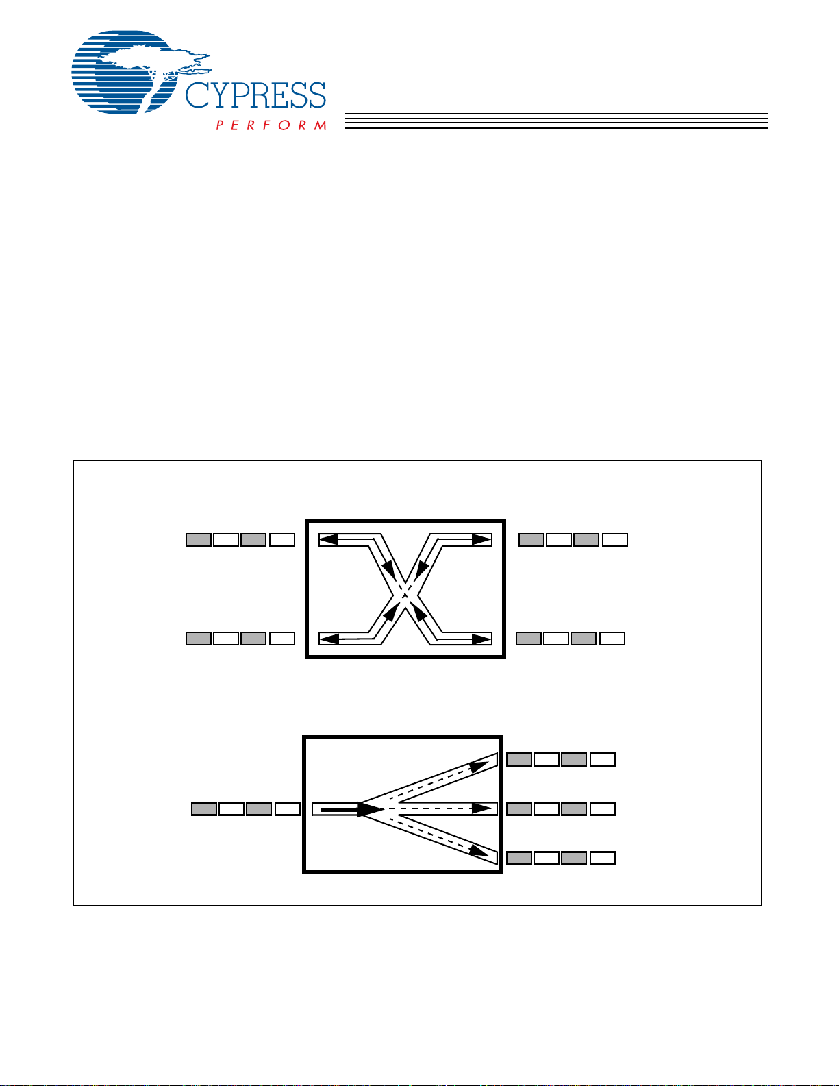
• QuadPort™ datapath switching element (DSE) family
allows four independent ports of access for data path
management and switching
• High-bandwidth data throughput up to 10 Gb/s
• 133-MHz
• High-speed clock to data access 4.2 ns (max.)
• Synchronous pipelined device
— 1-Mb (64K × 18) switch array
• 0.25-micron CMOS for optimum speed/power
• IEEE 1149.1 JTAG boundary scan
• Width and depth expansion capabilities
• BIST (Built-In Self-Test) controller
[1]
port speed x 18-bit-wide interface × 4 ports
QuadPort DSE Family Applications
PORT 1
• Dual Chip Enables on all ports for easy depth expansion
• Separate upper-byte and lower-byte controls on all
ports
• Simple array partitioning
— Internal mask register controls counter wrap-around
— Counter-Interrupt flags to indicate wrap-around
— Counter and mask registers readback on address
• 272-ball BGA package (27-mm × 27-mm × 1.27-mm ball
pitch)
• Commercial and industrial temperature ranges
• 3.3V low operating power
— Active = 750 mA (maximum)
— Standby = 15 mA (maximum
PORT 3
PORT 2
PORT 1 PORT 3
Note:
for commercial is 135 MHz and for industrial is 133 MHz.
1. f
MAX2
PORT 4
BUFFERED SWITCH
PORT 2
PORT 4
REDUNDANT DATA MIRROR
Cypress Semiconductor Corporation • 198 Champion Court • San Jose, CA 95134-1709 • 408-943-2600
Document #: 38-06027 Rev. *B Revised May 23, 2006
[+] Feedback
Page 2
CY7C0430BV
CY7C0430CV
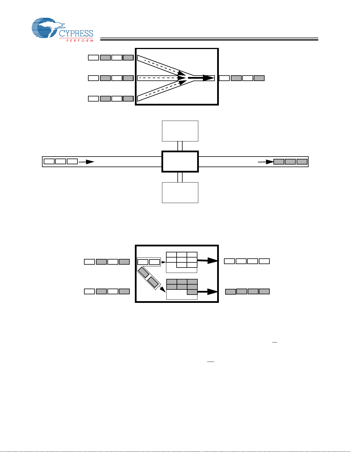
PORT 1
PORT 2
PORT 3
DATA PATH AGGREGATOR
Processor 1
Pre-processed DATA Path Processed DATA Path
PARALLEL PACKET PROCESSING
QuadPort
DSE Family
Processor 2
DATA PATH MANAGER FOR
PORT 4
PORT 1 PORT 3
PORT 2 PORT 4
DATA CLASSIFICATION ENGINE
Functional Description
The Quadport Datapath Switching Element (DSE) family offers
four ports that may be clocked at independent frequencies
from one another. Each port can read or write up to 133 MHz
giving the device up to 10 Gb/s of data throughput. The device
is 1-Mb (64K × 18) in density. Simultaneous reads are allowed
for accesses to the same address location; however, simultaneous reading and writing to the same address is not allowed.
Any port can write to a certain location while other ports are
reading that location simultaneously, if the timing spec for port
to port delay (t
location by more than one port at the same time is undefined.
Data is registered for decreased cycle time. Clock to data valid
t
= 4.2 ns. Each port contains a burst counter on the input
CD2
) is met. The result of writing to the same
CCS
[1]
Queue #1
Queue #2
address register. After externally loading the counter with the
initial address the counter will self-increment the address internally (more details to follow). The internal write pulse width is
independent of the duration of the R/W
internal write pulse is self-timed to allow the shortest possible
,
cycle times.
A HIGH on CE
down the internal circuitry to reduce the static power
consumption. One cycle is required with chip enables asserted
to reactivate the outputs.
The CY7C0430BV and CY7C0430CV (64K × 18 device)
supports burst contains for simple array partitioning. Counter
enable inputs are provided to stall the operation of the address
input and utilize the internal address generated by the internal
counter for fast interleaved memory applications. A port’s burst
or LOW on CE1 for one clock cycle will power
0
input signal. The
Document #: 38-06027 Rev. *B Page 2 of 37
[+] Feedback
Page 3
CY7C0430BV
CY7C0430CV
counter is loaded with an external address when the port’s
Counter Load pin (CNTLD
Counter Increment pin (CNTINC
) is asserted LOW. When the port’s
) is asserted, the address
counter will increment on each subsequent LOW-to- HIGH
transition of that port’s clock signal. This will read/write one
word from/into each successive address location until
CNTINC
is deasserted. The counter can address the entire
switch array and will loop back to the start. Counter Reset
(CNTRST) is used to reset the burst counter. A counter-mask
register is used to control the counter wrap. The counter and
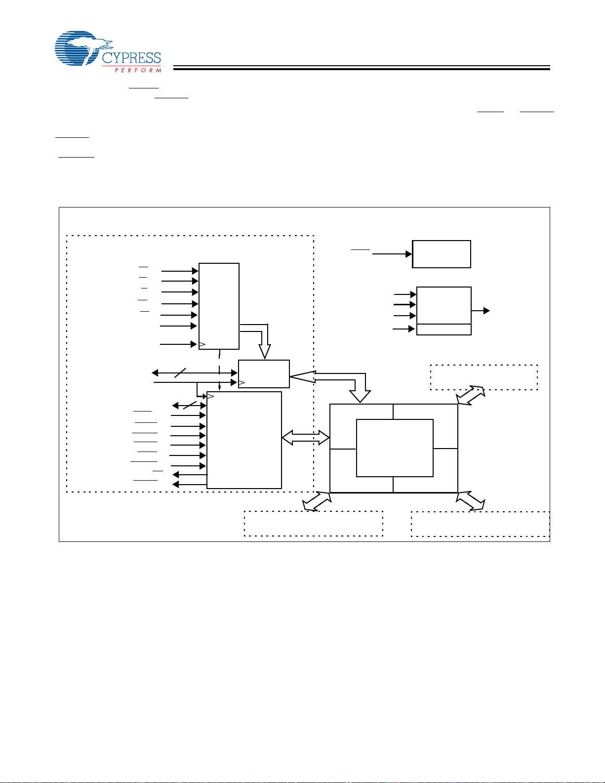
Top Level Logic Block Diagram
Port 1 Operation-control Logic Blocks
UB
P1
LB
P1
R/W
P1
OE
P1
CE
0P1
CE
1P1
CLK
P1
18
I/O
- I/O
0P1
17P1
CLK
P1
A
0P1–A15P1
MKLD
CNTLD
CNTINC
CNTRD
MKRD
CNTRST
CNTINT
P1
INT
16
P1
P1
P1
P1
P1
P1
P1
[2]
Port-1
Control
Logic
Port 1
I/O
Port 1
Counter/
Mask Reg/
Address
Decode
mask register operations are described in more details in the
following sections.
The counter or mask register values can be read back on the
bidirectional address lines by activating MKRD
or CNTRD,
respectively.
The new features included for the QuadPort DSE family
include: readback of burst-counter internal address value on
address lines, counter-mask registers to control the counter
wrap-around, readback of mask register value on address
lines, interrupt flags for message passing, BIST, JTAG for
boundary scan, and asynchronous Master Reset.
MRST
TMS
TCK
TDI
CLKBIST
Port 1
Reset
Logic
JTAG
Controller
BIST
Port 4 Logic Blocks
Port 4
TDO
[3]
64K × 18
QuadPort DSE
Array
Port 2
Port 3
Port 2 Logic Blocks
Notes:
2. Port 1 Control Logic Block is detailed on page 4.
3. Port 2, Port 3, and Port 4 Logic Blocks are similar to Port 1 Logic Blocks.
[3]
Port 3 Logic Blocks
[3]
Document #: 38-06027 Rev. *B Page 3 of 37
[+] Feedback
Page 4
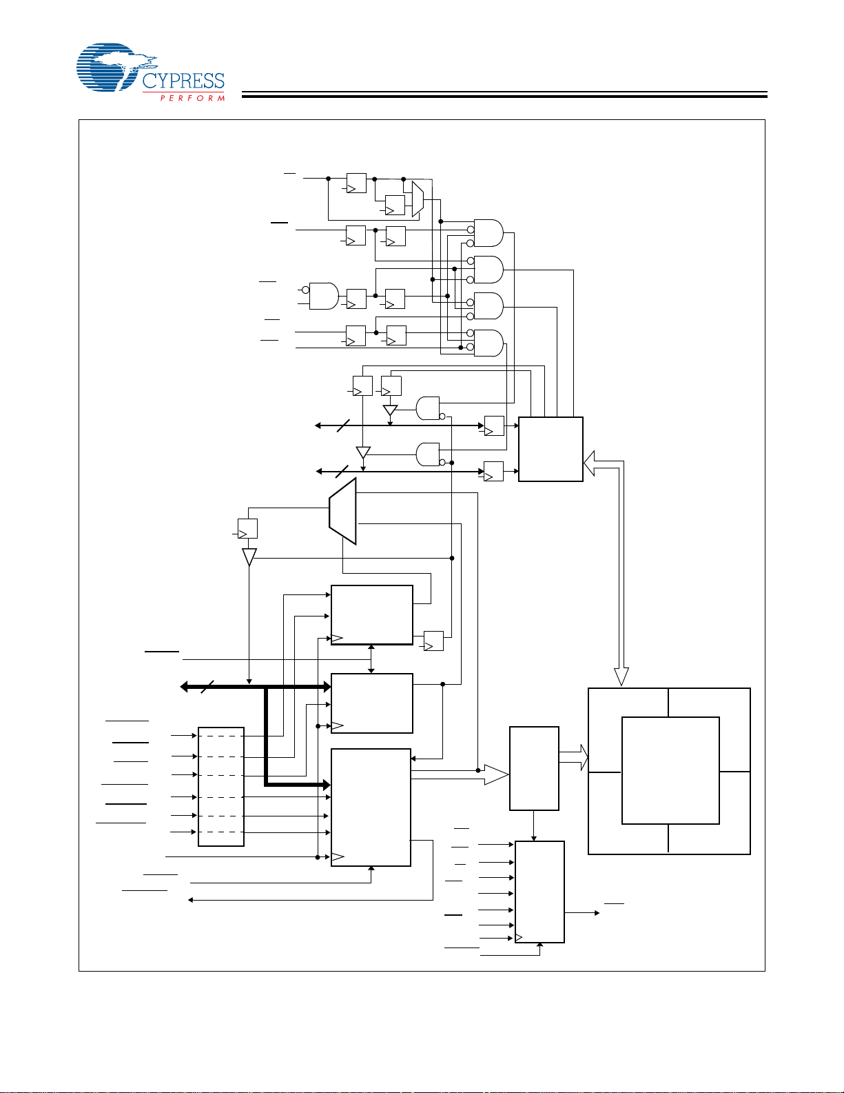
Port 1 Operation-Control Logic Block Diagram
(Address Readback is independent of CEs)
R/W
CE
CE
LB
OE
UB
0P1
1P1
P1
P1
P1
P1
W
CY7C0430BV
CY7C0430CV
A
0P1–A15P1
CNTRD
MKRD
MKLD
CNTINC
CNTLD
CNTRST
CLK
CNTINT
MRST
P1
P1
P1
P1
P1
P1
P1
MRST
P1
I/O
16
Priority
Decision
Logic
I/O
9P1
0P1
–I/O
–I/O
17P1
8P1
9
9
Addr.
Read
Port 1
Readback
Register
Port 1
Mask Register
Port 1
Counter/
Address
Register
LB
UB
R/W
CE
0P1
CE
1P1
OE
P1
CLK
MRST
P1
P1
P1
P1
Port-1
I/O
Control
Port 1
Address
Decode
Port 1
Interrupt
Logic
P
Po
or
r
t 2
INT
1
t
64K × 18
QuadPort
DSE Array
P1
P
ort 4
ort 3
P
Document #: 38-06027 Rev. *B Page 4 of 37
[+] Feedback
Page 5
CY7C0430BV
CY7C0430CV
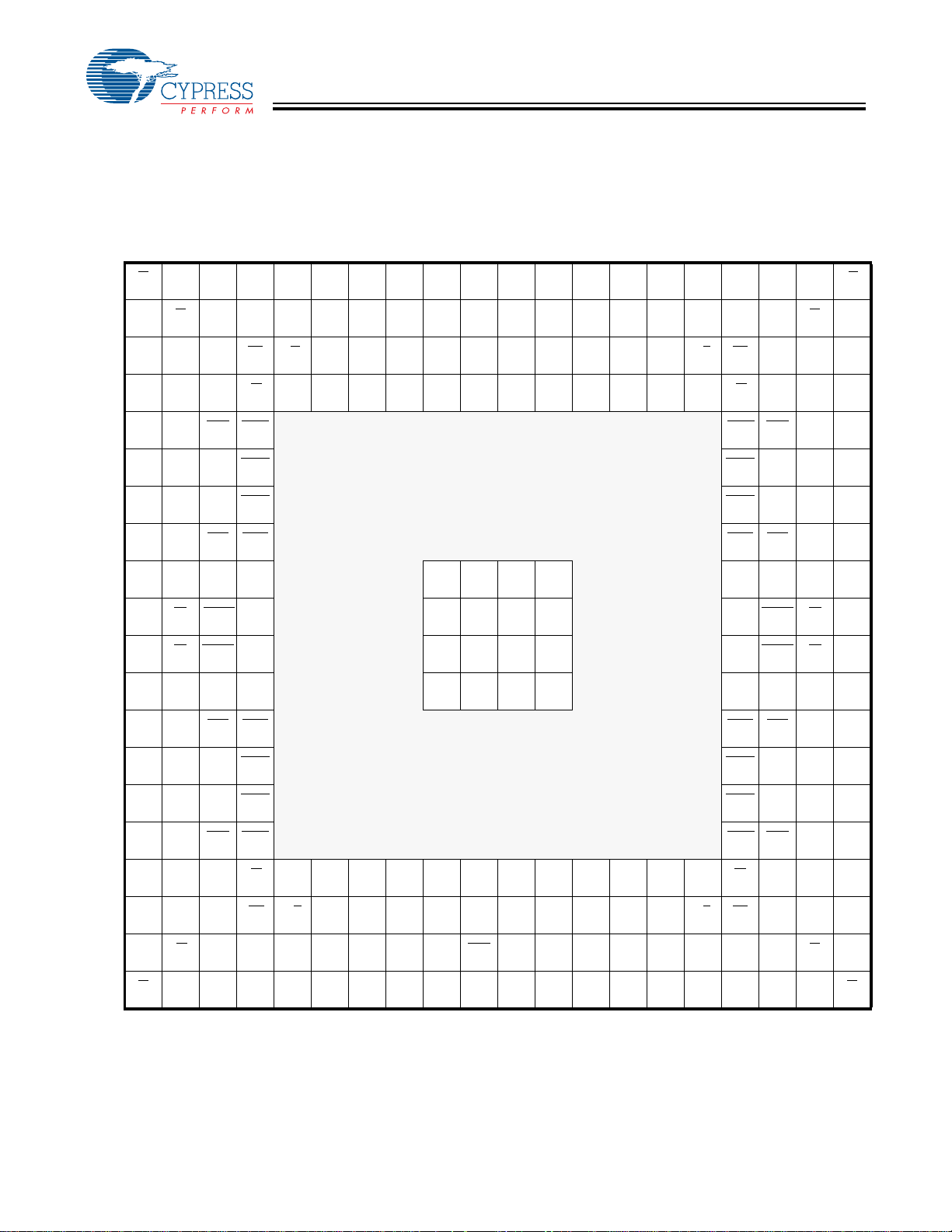
Pin Configuration
272-ball Grid Array (BGA)
Top Vi e w
1234567891011121314151617181920
LBP1I/O17P2I/O15P2I/O13P2I/O11P2I/O9P2I/O16P1I/O14P1I/O12P1I/O10P1I/O10P4I/O12P4I/O14P4I/O16P4I/O9P3I/O11P3I/O13P3I/O15P3I/O17P3 LB
A
VDD1 UBP1I/O16P2I/O14P2I/O12P2I/O10P2I/O17P1I/O13P1I/O11P1TMS TDI I/O11P4I/O13P4I/O17P4I/O10P3I/O12P3I/O14P3I/O16P3UBP4VDD1
B
A14P1A15P1CE1P1CE0P1R/WP1I/O15P1VSS2 VSS2 I/O9P1 TCK TDO I/O9P4VSS2 VSS2 I/O15P4R/WP4CE0P4CE1P4A15P4A14
C
P4
P4
VSS1 A12P1A13P1 OE
D
A10P1A11P1MKRD
E
A7P1A8P1A9P1CNTINT
F
VSS1 A5P1A6P1CNTINC
G
A3P1A4P1MKLDP1CNTLD
H
VDD1 A1P1A2P1VDD GND
J
A0P1INTP1 CNTRSTP1CLK
K
A0P2INTP2CNTRSTP2 VSS GND
L
VDD1 A1P2A2P2CLK
M
A3P2A4P2MKLDP2CNTLD
N
VSS1 A5P2A6P2CNTINC
P
A7P2A8P2A9P2CNTINT
R
A10P2A11P2MKRD
T
P1
P2
VDD2 VSS2 VSS2 VDD2 VDD VSS VSS VDD VDD2 VSS2 VSS2 VDD2 OEP4A13P4A12P4VSS1
P1
CNTRD
P1
P1
P1
P1
P1
P2
P2
P2
P2
CNTRD
P2
GND
GND
MKRDP4A11P4A10
CNTRD
P4
CNTINT
P4A9P4A8P4
CNTINCP4A6P4A5P4 VSS1
CNTLDP4MKLDP4A4P4A3
[4]
[4]
[4]
GND
GND
[4]
[4]
GND
GND
[4]
[4]
GND
GND
[4]
[4]
GND
GND
[4]
GND
[4]
[4]
GND
[4]
[4]
GND
[4]
[4]
GND
VDD A2P4A1P4VDD1
CLKP4CNTRSTP4INTP4 A0
VSS CNTRSTP3INTP3 A0
CLKP3A2P3A1P3VDD1
CNTLDP3MKLDP3A4P3A3
CNTINC
P3A6P3A5P3
CNTINTP3A9P3A8P3 A7
MKRDP3A11P3A10
CNTRD
P3
P4
A7
P4
P4
P4
P3
P3
VSS1
P3
P3
VSS1 A12P2A13P2 OE
U
A14P2A15P2CE1P2 CE0
V
VDD1 UB
W
Y
P2
I/O8P1I/O6P1I/O4P1I/O2P1I/O0P11/O7P2I/O5P2I/O3P2I/O1P2I/O1P3I/O3P3I/O5P3I/O7P3I/O0P4I/O2P4I/O4P4I/O6P4I/O8P4LB
LB
P2
I/O7P1I/O5P1I/O3P1I/O1P1I/O8P2I/O4P2I/O2P2MRST
VDD2 VSS2 VSS2 VDD2 VDD VSS VSS VDD VDD2 VSS2 VSS2 VDD2 OEP3A13P3A12P3VSS1
P2
R/WP2I/O6P2VSS2 VSS2 I/O0P2NC NC I/O0P3VSS2 VSS2 I/O6P3R/WP3CE0P3CE1P3A15P3A14
P2
CLKBIST I/O2P3I/O4P3I/O8P3I/O1P4I/O3P4I/O5P4I/O7P4UB
P3
VDD1
P3
P3
Note:
4. Central Leads are for thermal dissipation only. They are connected to device V
.
SS
Document #: 38-06027 Rev. *B Page 5 of 37
[+] Feedback
Page 6
CY7C0430BV
CY7C0430CV
Selection Guide
CY7C0430CV
–133
f
MAX2
133
[1]
Max Access Time (Clock to Data) 4.2 5.0 ns
Max Operating Current I
Max Standby Current for I
Max Standby Current for I
CC
(All ports TTL Level) 200 150 mA
SB1
(All ports CMOS Level) 15 15 mA
SB3
750 600 mA
Pin Definitions
Port 1 Port 2 Port 3 Port 4 Description
A
0P1–A15P1
I/O
–I/O
0P1
CLK
P1
LB
P1
UB
P1
CE
,CE
0P1
OE
P1
R/W
P1
MRST Master Reset Input. This is one signal for All Ports.
CNTRST
MKLD
CNTLD
CNTINC
P1
P1
P1
P1
17P1
1P1
A
0P2–A15P2
I/O
–I/O
0P2
CLK
P2
LB
P2
UB
P2
CE
,CE
0P2
OE
P2
R/W
P2
CNTRST
MKLD
P2
CNTLD
CNTINC
P2
P2
1P2
P2
17P2
A
0P3–A15P3
I/O
–I/O
0P3
CLK
P3
LB
P3
UB
P3
CE
,CE
0P3
OE
P3
R/W
P3
CNTRST
MKLD
P3
CNTLD
CNTINC
P3
P3
1P3
P3
17P3
A
0P4–A15P4
I/O
–I/O
0P4
CLK
P4
LB
P4
UB
P4
CE
,CE
0P4
OE
P4
R/W
P4
CNTRST
MKLD
P4
CNTLD
CNTINC
P4
P4
P4
Address Input/Output.
Data Bus Input/Output.
17P4
Clock Input. This input can be free running or strobed.
Maximum clock input rate is f
Lower Byte Select Input. Asserting this signal LOW
enables read and write operations to the lower byte. For
read operations both the LB and OE signals must be
asserted to drive output data on the lower byte of the data
pins.
Upper Byte Select Input. Same function as LB, but to the
upper byte.
Chip Enable Input. To select any port, both CE0 AND
1P4
CE
must be asserted to their active states (CE0 ≤ VIL and
1
CE
≥ VIH).
1
Output Enable Input. This signal must be asserted LOW
to enable the I/O data lines during read operations. OE
asynchronous input.
Read/Write Enable Input. This signal is asserted LOW
to write to the dual port memory array. For read operations, assert this pin HIGH.
MRST
is an asynchronous input. Asserting MRST LOW
performs all of the reset functions as described in the text.
A MRST
operation is required at power-up.
Counter Reset Input. Asserting this signal LOW resets
the burst address counter of its respective port to zero.
CNTRST
is second to MRST in priority with respect to
counter and mask register operations.
Mask Register Load Input. Asserting this signal LOW
loads the mask register with the external address
available on the address lines. MKLD
higher priority over CNTLD
Counter Load Input. Asserting this signal LOW loads the
burst counter with the external address present on the
address pins.
Counter Increment Input. Asserting this signal LOW
increments the burst address counter of its respective port
on each rising edge of CLK.
CY7C0430CV
–100 Unit
100 MHz
.
MAX
operation has
operation.
is
Document #: 38-06027 Rev. *B Page 6 of 37
[+] Feedback
Page 7
CY7C0430BV
CY7C0430CV
Pin Definitions (continued)
Port 1 Port 2 Port 3 Port 4 Description
CNTRD
MKRD
CNTINT
P1
P1
P1
INTP1 INTP2 INTP3 INTP4 Interrupt Flag Output. Interrupt permits communications
TMS JTAG Test Mode Select Input. It controls the advance of
TCK JTAG Test Clock Input. This can be CLK of any port or
TDI JTAG Test Data Input. This is the only data input. TDI
TDO JTAG Test Data Output. This is the only data output.
CLKBIST BIST Clock Input.
GND Thermal Ground for Heat Dissipation.
V
SS
V
DD
V
SS1
V
DD1
V
SS2
V
DD2
CNTRD
MKRD
CNTINT
P2
P2
P2
CNTRD
MKRD
CNTINT
P3
P3
P3
CNTRD
MKRD
CNTINT
P4
P4
P4
Counter Readback Input. When asserted LOW, the
internal address value of the counter will be read back on
the address lines. During CNTRD
and CNTINC
must be HIGH. Counter readback operation
operation, both CNTLD
has higher priority over mask register readback operation.
Counter readback operation is independent of port chip
enables. If address readback operation occurs with chip
enables active (CE0 = LOW, CE1 = HIGH), the data lines
(I/Os) will be three-stated. The readback timing will be
valid after one no-operation cycle plus t
edge of the next cycle.
from the rising
CD2
Mask Register Readback Input. When asserted LOW,
the value of the mask register will be readback on address
lines. During mask register readback operation, all
counter and MKLD
inputs must be HIGH (see Counter
and Mask Register Operations truth table). Mask register
readback operation is independent of port chip enables.
If address readback operation occurs with chip enables
active (CE
be three-stated. The readback will be valid after one
no-operation cycle plus t
next cycle.
= LOW, CE1 = HIGH), the data lines (I/Os) will
0
from the rising edge of the
CD2
Counter Interrupt Flag Output. Flag is asserted LOW
for one clock cycle when the counter wraps around to
location zero.
between all four ports. The upper four memory locations
can be used for message passing. Example of operation:
INT
is asserted LOW when another port writes to the
P4
mailbox location of Port 4. Flag is cleared when Port 4
reads the contents of its mailbox. The same operation is
applicable to ports 1, 2, and 3.
JTAG TAP state machine. State machine transitions occur
on the rising edge of TCK.
an external clock connected to the JTAG TAP.
inputs will shift data serially in to the selected register.
TDO transitions occur on the falling edge of TCK. TDO
normally three-stated except when captured data is
shifted out of the JTAG TAP.
Ground Input.
Power Input.
Address Lines Ground Input.
Address Lines Power Input.
Data Lines Ground Input.
Data Lines Power Input.
Document #: 38-06027 Rev. *B Page 7 of 37
[+] Feedback
Page 8
Maximum Ratings
CY7C0430BV
CY7C0430CV
(Above which the useful life may be impaired. For user guidelines, not tested.)
Storage Temperature ................................ –65
°C to + 150°C
Ambient Temperature with
Power Applied............................................–55
°C to + 125°C
Supply Voltage to Ground Potential.............. –0.5V to + 4.6V
DC Voltage Applied to
Outputs in High-Z State..........................–0.5V to V
DC Input Voltage....................................–0.5V to V
CC
CC
+ 0.5V
+ 0.5V
Electrical Characteristics Over the Operating Range
Parameter Description
V
V
V
V
I
I
I
I
I
I
OH
OL
IH
IL
OZ
CC
SB1
SB2
SB3
SB4
Output HIGH Voltage
(V
= Min., I
CC
= –4.0 mA)
OH
Output LOW Voltage
(V
= Min., I
CC
= +4.0 mA)
OH
Input HIGH Voltage 2.0 2.0 V
Input LOW Voltage 0.8 0.8 V
Output Leakage Current –10 10 –10 10 µA
Operating Current (V
Outputs Disabled, CE
= Max., I
CC
= VIL, f = f
OUT
max
= 0 mA)
Standby Current (four ports toggling at TTL
Levels,0 active)
CE
≥ VIH, f = f
1-4
Standby Current (four ports toggling at TTL
Levels, 1 active)
f = f
MAX
Standby Current (four ports CMOS Level, 0
active)
CE
MAX
CE1 | CE2 | CE3 | CE4 < VIL,
≥ VIH, f = 0
1–4
Standby Current (four ports CMOS Level, 1
active and toggling) CE
, f = f
V
IL
MAX
| CE2 | CE3 | CE4 <
1
Output Current into Outputs (LOW)............................. 20 mA
Static Discharge Voltage........................................... > 2200V
Latch-up Current.....................................................> 200 mA
Operating Range
Range Ambient Temperature V
Commercial 0°C to +70°C 3.3V ± 150 mV
Industrial –40
°C to +85°C 3.3V ± 150 mV
Quadport DSE Family
–133 –100
Min. Typ. Max. Min. Typ. Max.
2.4 2.4 V
0.4 0.4 V
350 700 300 550 mA
80 200 60 150 mA
150 300 125 250 mA
1.5 15 1.5 15 mA
110 290 85 240 mA
DD
Unit
JTAG TAP Electrical Characteristics Over the Operating Range
Parameter Description Test Conditions Min. Max. Unit
V
V
V
V
I
OH1
OL1
IH
IL
X
Output HIGH Voltage I
= −4.0 mA 2.4 V
OH
Output LOW Voltage IOL = 4.0 mA 0.4 V
Input HIGH Voltage 2.0 V
Input LOW Voltage 0.8 V
Input Leakage Current GND ≤ VI ≤ V
DD
–100 100 µA
Capacitance
Parameter Description Test Conditions Max. Unit
CIN (All Pins) Input Capacitance TA = 25°C, f = 1 MHz,
V
= 3.3V
C
(All Pins) Output Capacitance 10 pF
OUT
CC
CIN (CLK Pins) Input Capacitance 15 pF
C
(CLK Pins) Output Capacitance 15 pF
OUT
Document #: 38-06027 Rev. *B Page 8 of 37
10 pF
[+] Feedback
Page 9
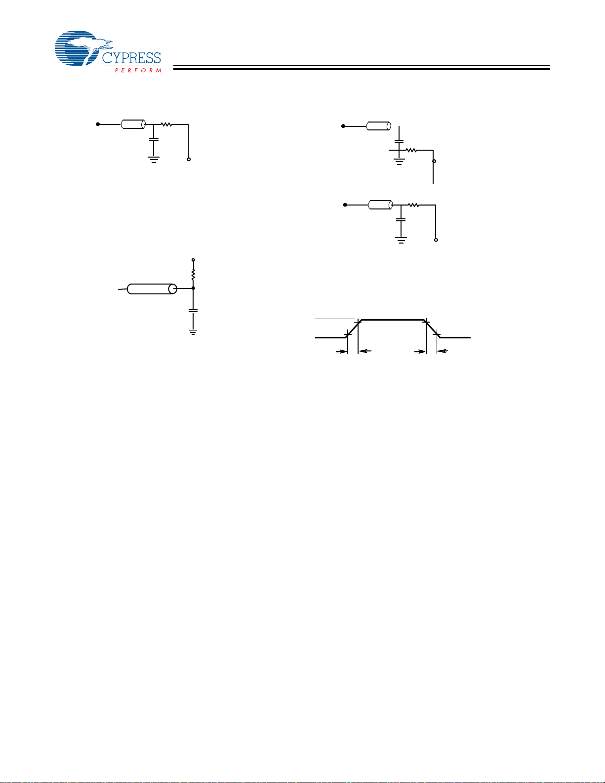
AC Test Load
CY7C0430BV
CY7C0430CV
OUTPUT
Z0 = 50Ω
C
(a) Normal Load
TDO
Z
Note:
5. Test conditions: C = 10 pF.
R = 50Ω
[5]
=50Ω
0
(c) TAP Load
VTH=1.5V
1.5V
50Ω
C
GND
= 10 pF
OUTPUT
OUTPUT
3.0V
GND
Z0 = 50Ω
5 pF
Z0 = 50Ω
5 pF
(b) Three-State Delay
10%
t
R
90%
All Input Pulses
R = 50Ω
R = 50Ω
VTH=1.5V
VTH=3.3V
90%
10%
t
F
Document #: 38-06027 Rev. *B Page 9 of 37
[+] Feedback
Page 10

CY7C0430BV
CY7C0430CV
Switching Characteristics Over the Industrial Operating Range
Parameter Description
[7]
f
MAX2
[7]
t
CYC2
t
CH2
t
CL2
t
R
t
F
t
SA
t
HA
t
SC
t
HC
t
SW
t
HW
t
SD
t
HD
t
SB
t
HB
t
SCLD
t
HCLD
t
SCINC
t
HCINC
t
SCRST
t
HCRST
t
SCRD
t
HCRD
t
SMLD
t
HMLD
t
SMRD
t
HMRD
t
OE
[8]
t
OLZ
[8]
t
OHZ
t
CD2
t
CA2
t
CM2
t
DC
[9]
t
CKHZ
Notes:
6. If data is simultaneously written and read to the same address location and t
remaining in the address is undefined.
7. f
MAX2
8. This parameter is guaranteed by design, but it is not production tested.
9. Valid for both address and data outputs.
Maximum Frequency 133 100 MHz
Clock Cycle Time 7.5 10 ns
Clock HIGH Time 3 4 ns
Clock LOW Time 3 4 ns
Clock Rise Time 2 3 ns
Clock Fall Time 2 3 ns
Address Set-up Time 2.3 3 ns
Address Hold Time 0.7 0.7 ns
Chip Enable Set-up Time 2.3 3 ns
Chip Enable Hold Time 0.7 0.7 ns
R/W Set-up Time 2.3 3 ns
R/W Hold Time 0.7 0.7 ns
Input Data Set-up Time 2.3 3 ns
Input Data Hold Time 0.7 0.7 ns
Byte Set-up Time 2.3 3 ns
Byte Hold Time 0.7 0.7 ns
CNTLD Set-up Time 2.3 3 ns
CNTLD Hold Time 0.7 0.7 ns
CNTINC Set-up Time 2.3 3 ns
CNTINC Hold Time 0.7 0.7 ns
CNTRST Set-up Time 2.3 3 ns
CNTRST Hold Time 0.7 0.7 ns
CNTRD Set-up Time 2.3 3 ns
CNTRD Hold Time 0.7 0.7 ns
MKLD Set-up Time 2.3 3 ns
MKLD Hold Time 0.7 0.7 ns
MKRD Set-up Time 2.3 3 ns
MKRD Hold Time 0.7 0.7 ns
Output Enable to Data Valid 6.5 8 ns
OE to Low-Z 1 1 ns
OE to High-Z 1 6 1 7 ns
Clock to Data Valid 4.2 5 ns
Clock to Counter Address Readback Valid 4.7 5 ns
Clock to Mask Register Readback Valid 4.7 5 ns
Data Output Hold After Clock HIGH 1 1 ns
Clock HIGH to Output High-Z 1 4.8 1 6.8 ns
is violated, the data read from the address, as well as the subsequent data
CCS
for commercial is 135 MHz. t
Min. for commercial is 7.4 ns.
CYC2
[6]
CY7C0430BV and CY7C0430CV
–133 –100
Min. Max. Min. Max.
Unit
Document #: 38-06027 Rev. *B Page 10 of 37
[+] Feedback
Page 11
CY7C0430BV
CY7C0430CV
Switching Characteristics Over the Industrial Operating Range (continued)
CY7C0430BV and CY7C0430CV
–133 –100
Parameter Description
[9]
t
CKLZ
t
SINT
t
RINT
t
SCINT
t
RCINT
Clock HIGH to Output Low-Z 1 1 ns
Clock to INT Set Time 1 7.5 1 10 ns
Clock to INT Reset Time 1 7.5 1 10 ns
Clock to CNTINT Set Time 1 7.5 1 10 ns
Clock to CNTINT Reset Time 1 7.5 1 10 ns
Min. Max. Min. Max.
Master Reset Timing
t
RS
t
RSR
t
ROF
Master Reset Pulse Width 7.5 10 ns
Master Reset Recovery Time 7.5 10 ns
Master Reset to Output Flags Reset Time 6.5 8 ns
Port to Port Delays
[6]
t
CCS
Clock to Clock Set-up Time (time required after a write
before you can read the same address location)
6.5 9 ns
JTAG Timing and Switching Waveforms
Parameter Description
f
JTAG
t
TCYC
t
TH
t
TL
t
TMSS
t
TMSH
t
TDIS
t
TDIH
t
TDOV
t
TDOX
f
BIST
t
BH
t
BL
Maximum JTAG TAP Controller Frequency 10 MHz
TCK Clock Cycle Time 100 ns
TCK Clock High Time 40 ns
TCK Clock Low Time 40 ns
TMS Set-up to TCK Clock Rise 20 ns
TMS Hold After TCK Clock Rise 20 ns
TDI Set-up to TCK Clock Rise 20 ns
TDI Hold after TCK Clock Rise 20 ns
TCK Clock Low to TDO Valid 20 ns
TCK Clock Low to TDO Invalid 0 ns
Maximum CLKBIST Frequency 50 MHz
CLKBIST High Time 6 ns
CLKBIST Low Time 6 ns
Min. Max.
[6]
Unit
Quadport DSE Family
–133/–100
Unit
Document #: 38-06027 Rev. *B Page 11 of 37
[+] Feedback
Page 12
t
CY7C0430BV
CY7C0430CV
Test Clock
TCK
Test Mode Select
TMS
Test Data-In
TDI
Test Data-Out
TDO
Switching Waveforms
Master Reset
CLK
[10]
t
CH2
t
CYC2
t
TMSS
t
CL2
t
TDIS
TH
t
TDOX
t
TDOV
t
TL
t
TMSH
t
TDIH
t
TCYC
t
MRST
t
ALL
ADDRESS/
DATA
LINES
ALL
OTHER
INPUTS
[11]
TMS
CNTINT
INT
TDO
Notes:
is the set-up time required for all input control signals.
10. t
S
11.To Reset the test port without resetting the device, TMS must be held low for five clock cycles.
RSF
RS
t
RSR
INACTIVE
t
S
ACTIVE
Document #: 38-06027 Rev. *B Page 12 of 37
[+] Feedback
Page 13

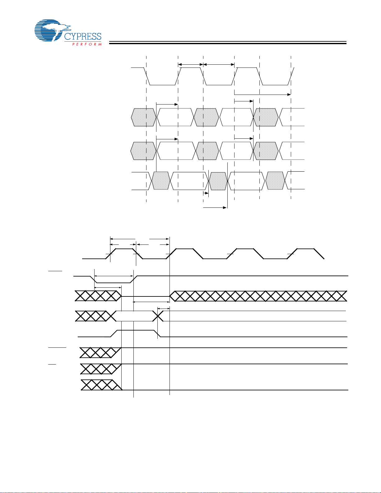
Switching Waveforms (continued)
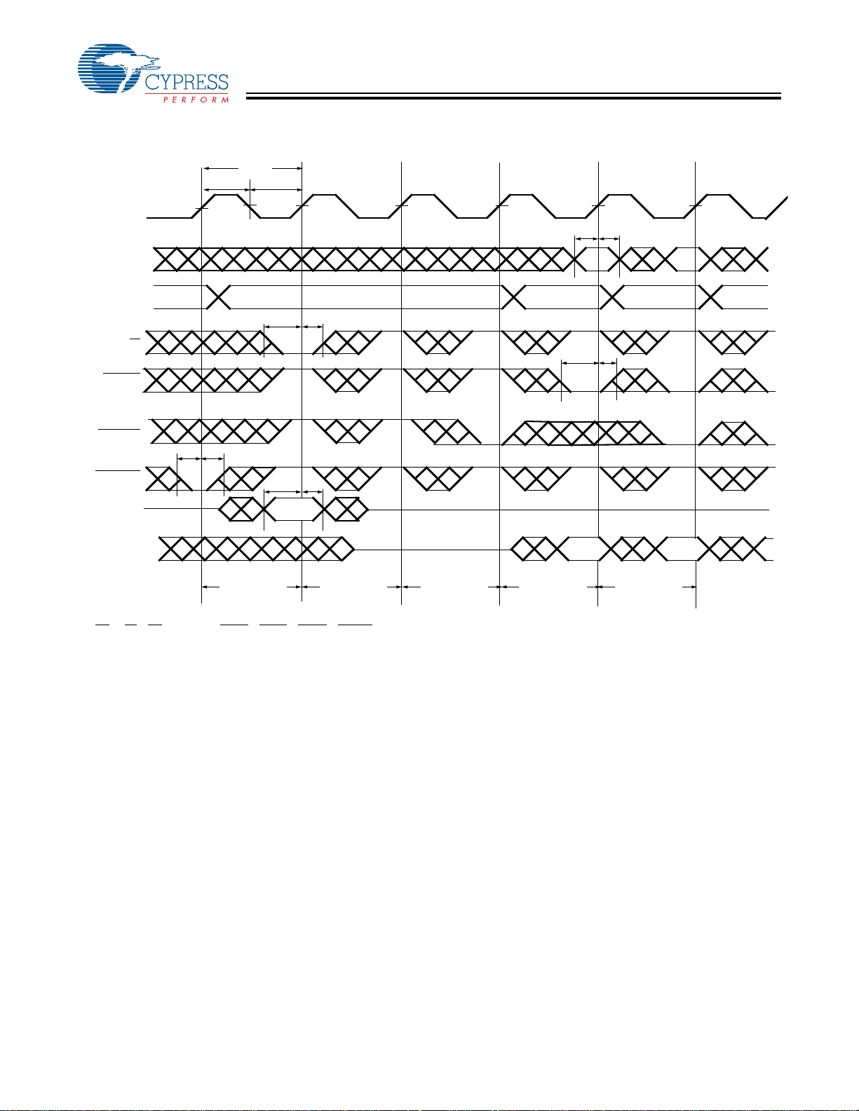
Read Cycle
[12, 13, 14, 15, 16]
CLK
CE
t
t
CH2
CYC2
t
CL2
CY7C0430BV
CY7C0430CV
t
SC
t
HC
t
SC
t
HC
LB
t
SB
t
HB
UB
R/W
ADDRESS
DATA
OUT
t
t
SW
SA
t
HW
t
HA
A
n
1 Latency
t
CKLZ
A
n+1
t
CD2
A
n+2
t
DC
Q
n
A
n+3
Q
n+1
t
OHZ
t
OLZ
Q
n+2
OE
t
OE
Notes:
12. OE
is asynchronously controlled; all other inputs (excluding MRST) are synchronous to the rising clock edge.
13. CNTLD
14. The output is disabled (high-impedance state) by CE
15. Addresses do not have to be accessed sequentially. Note 13 indicates that address is constantly loaded on the rising edge of the CLK. Numbers are for reference
16. CE
= VIL, MKLD = VIH, CNTINC = x, and MRST = CNTRST = VIH.
only.
is internal signal. CE = VIL if CE0 = VIL and CE1 = VIH.
= VIH following the next rising edge of the clock.
Document #: 38-06027 Rev. *B Page 13 of 37
[+] Feedback
Page 14

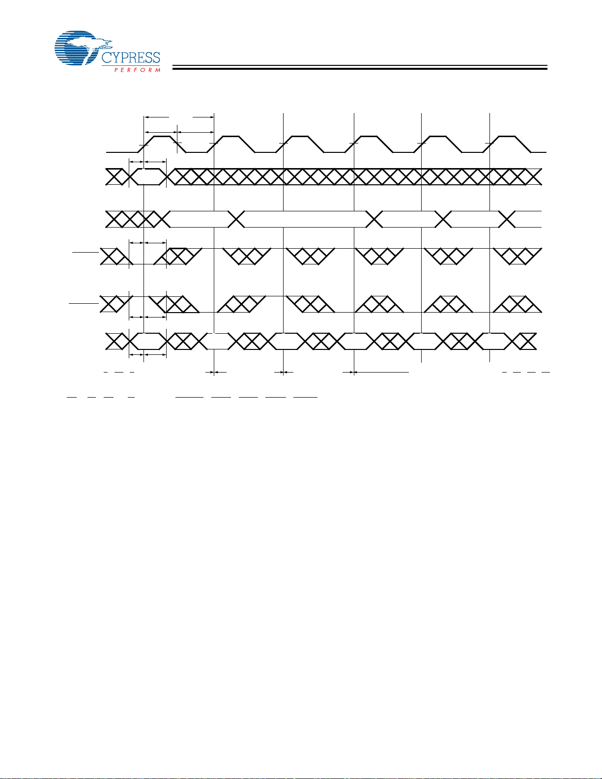
Switching Waveforms (continued)
t
SA
t
SC
[17, 18]
t
CYC2
t
CH2
A
0
t
CL2
t
HA
t
HC
Bank Select Read
CLK
ADDRESS
CE
(B1)
(B1)
CY7C0430BV
CY7C0430CV
A
1
t
CD2
A
2
t
t
t
SC
HC
CD2
A
3
t
CKHZ
A
4
t
CD2
A
5
t
CKHZ
DATA
OUT(B1)
ADDRESS
CE
DATA
OUT(B2)
(B2)
(B2)
t
SA
A
t
SC
t
HA
0
t
HC
Read-to-Write-to-Read (OE = VIL)
t
CYC2
t
CH2
CLK
CE
R/W
t
SC
t
SW
t
t
HC
HW
A
[19, 20, 21, 22]
t
CL2
Q
0
t
DC
SC
A
2
t
HC
t
HW
1
t
t
SW
Q
1
t
DC
A
3
t
CD2
t
CKLZ
t
CKLZ
A
4
t
CKHZ
Q
2
Q
3
A
5
t
CD2
Q
4
t
CKLZ
ADDRESS
DATA
DATA
OUT
A
n
t
SA
IN
t
HA
A
n+1
t
CD2
A
n+2
t
CKHZ
Q
n
A
n+2
tSDt
D
n+2
HD
A
n+3
t
CKLZ
A
n+4
t
CD2
Q
n+3
No Operation WriteRead Read
Notes:
17. In this depth expansion example, B1 represents Bank #1 and B2 is Bank #2; Each bank consists of one QuadPort DSE device from this data sheet.
ADDRESS
= UB = OE = CNTLD = VIL; MRST = CNTRST= MKLD = VIH.
18. LB
19. Output state (HIGH, LOW, or high-impedance) is determined by the previous cycle control signals.
= UB = CNTLD = VIL; MRST = CNTRST = MKLD = VIH.
20. LB
21. Addresses do not have to be accessed sequentially since CNTLD
22. During “No Operation,” data in memory at the selected address may be corrupted and should be rewritten to ensure data integrity.
= ADDRESS
(B1)
(B2)
.
= VIL constantly loads the address on the rising edge of the CLK; numbers are for reference only.
Document #: 38-06027 Rev. *B Page 14 of 37
[+] Feedback
Page 15

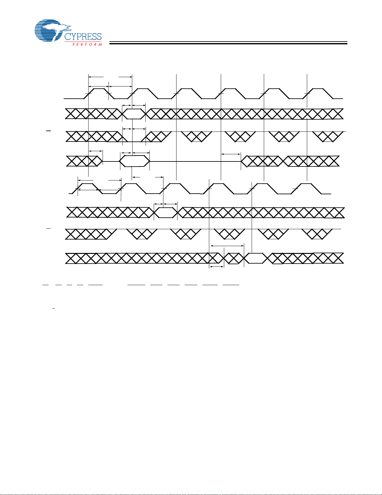
Switching Waveforms (continued)
Read-to-Write-to-Read (OE Controlled)
t
CYC2
t
CL2
CLK
t
CH2
[19, 20, 21, 22]
CY7C0430BV
CY7C0430CV
CE
t
HC
t
HW
n
R/W
t
SC
t
SW
A
ADDRESS
t
HA
DATA
DATA
OUT
t
SA
IN
OE
Read with Address Counter Advance
t
CYC2
CLK
t
CH2
t
CL2
t
t
HW
SW
A
n+1
t
CD2
Q
t
OHZ
A
n+2
tSDt
HD
D
n+2
n
A
n+3
D
Read ReadWrite
[23, 24]
n+3
A
n+4
t
CKLZ
A
n+5
t
CD2
Q
n+4
ADDRESS
t
SA
t
SCLD
A
t
HA
n
t
HCLD
CNTLD
CNTINC
DATA
OUT
Q
x–1
Read
External
t
SCINC
t
CD2
Q
x
t
DC
Read with Counter
t
HCINC
Q
n
Q
n+1
Counter Hold
Q
n+2
Read with Counter
Q
n+3
Address
Notes:
= OE = LB = UB = VIL; CE1 = R/W = CNTRST = MRST = MKLD = MKRD = CNTRD = VIH.
23. CE
0
24. The “Internal Address” is equal to the “External Address” when CNTLD
= VIL.
Document #: 38-06027 Rev. *B Page 15 of 37
[+] Feedback
Page 16
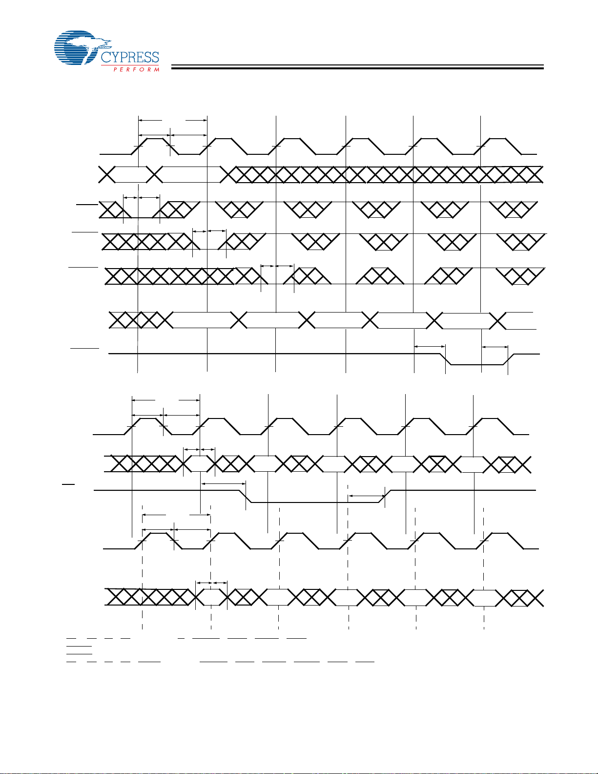
Switching Waveforms (continued)
Write with Address Counter Advance
t
CYC2
CLK
ADDRESS
t
CH2
t
SA
A
n
t
CL2
t
HA
[24, 25]
CY7C0430BV
CY7C0430CV
INTERNAL
ADDRESS
t
SCLD
t
HCLD
A
n
CNTLD
CNTINC
t
SCINC
DATA
IN
t
SD
Note:
= LB = UB = R/W = VIL; CE1 = CNTRST = MRST = MKLD = MKRD = CNTRD = V
25. CE
0
t
HCINC
D
n
t
HD
Write External
Address
D
n+1
Write with
Counter
A
n+1
D
n+1
Write Counter
Hold
A
n+2
D
n+2
D
n+3
A
n+3
D
n+4
A
n+4
Write with Counter
IH.
Document #: 38-06027 Rev. *B Page 16 of 37
[+] Feedback
Page 17
Switching Waveforms (continued)
Counter Reset
CLK
[21, 26, 27]
t
CH2
t
CYC2
t
CL2
CY7C0430BV
CY7C0430CV
tSAt
HA
ADDRESS
INTERNAL
ADDRESS
A
X
t
SWtHW
A
0
R/W
t
SCLD
CNTLD
CNTINC
t
SCRST
CNTRST
DATA
IN
DATA
OUT
Notes:
26. CE
= LB = UB = VIL; CE1 = MRST = MKLD = MKRD = CNTRD = VIH.
0
27. No dead cycle exists during counter reset. A Read or Write cycle may be coincidental with the counter reset.
t
HCRST
Counter
Reset
t
SDtHD
D
0
Write
Address 0
Read
Address 0
Read
Address 1
A
n
A
1
t
HCLD
Q
0
Address n
Read
A
n+1
A
n
Q
1
A
n+1
A
n+2
Q
n
Document #: 38-06027 Rev. *B Page 17 of 37
[+] Feedback
Page 18

Switching Waveforms (continued)
t
CYC2
HA
t
HCLD
t
[28]
CL2
Load and Read Address Counter
t
CH2
CLK
t
A
n
A
0–A15
CNTLD
CNTINC
t
SCLD
t
SA
CY7C0430BV
CY7C0430CV
Note 29
t
CKLZ
t
CA2
Note 30
t
CKHZ
[31]
A
n+2
t
SCINC
t
HCINC
CNTRD
INTERNAL
ADDRESS
DATA
OUT
Q
x–1
Load
External
A
n
t
CD2
Q
x
A
n+1
t
Q
n
Read Data with Counter
Address
Notes:
= OE = LB = UB = VIL; CE1 = R/W = CNTRST = MRST = MKLD = MKRD = VIH.
28. CE
0
29. Address in output mode. Host must not be driving address bus after time t
30. Address in input mode. Host can drive address bus after t
31. This is the value of the address counter being read out on the address lines.
CKHZ
.
t
SCRD
DC
in next clock cycle.
CKLZ
t
HCRD
A
n+2
Q
n+1
A
n+2
Q
n+2
t
CKHZ
A
n+2
t
CKLZ
Q
n+2
Read
Internal
Address
Document #: 38-06027 Rev. *B Page 18 of 37
[+] Feedback
Page 19
Switching Waveforms (continued)
t
CYC2
t
HA
t
HMLD
t
[32]
CL2
Load and Read Mask Register
t
CH2
CLK
t
SA
A
0–A15
MKLD
t
SMLD
A
n
CY7C0430BV
CY7C0430CV
Note 29
t
CKLZ
t
CA2
Note 30
t
CKHZ
[33]
A
n
MKRD
MASK
INTERNAL
VALUE
A
n
A
n
Load
Mask Register
Value
Notes:
= OE = LB = UB = VIL; CE1 = R/W = CNTRST = MRST = CNTLD = CNTRD = CNTINC =VIH.
32. CE
0
33. This is the value of the Mask Register read out on the address lines.
t
SMRD
t
HMRD
A
n
A
n
A
n
Read
Mask Register
Value
Document #: 38-06027 Rev. *B Page 19 of 37
[+] Feedback
Page 20
Switching Waveforms (continued)
t
CH2
[34, 35, 36]
t
CYC2
t
CL2
t
SA
A
Port 1 Write to Port 2 Read
CLK
P1
PORT-1
ADDRESS
CY7C0430BV
CY7C0430CV
t
HA
n
t
t
CYC2
t
CL2
SW
t
SD
D
n
R/W
P1
t
CKHZ
PORT-1
DATA
IN
CLK
P2
PORT-2
ADDRESS
R/W
P2
PORT-2
DATA
OUT
Notes:
34. CE
= OE = LB = UB = CNTLD =VIL; CE1 = CNTRST = MRST = MKLD = MKRD = CNTRD = CNTINC =VIH.
0
35. This timing is valid when one port is writing, and one or more of the three other ports is reading the same location at the same time. If t
data will be read out.
< minimum specified value, then Port 2 will read the most recent data (written by Port 1) only (2*t
36. If t
CCS
t
> minimum specified value, then Port 2 will read the most recent data (written by Port 1) (t
CCS
t
CH2
t
CCS
t
SA
t
HW
t
HD
t
CKLZ
t
HA
A
n
t
CD2
Q
n
t
DC
+ t
CYC2
+ t
CYC2
CD2
) after the rising edge of Port 2’s clock. If
CD2
) after the rising edge of Port 2’s clock.
is violated, indeterminate
CCS
Document #: 38-06027 Rev. *B Page 20 of 37
[+] Feedback
Page 21
Switching Waveforms (continued)
Counter Interrupt
CLK
[37, 38, 39]
t
CH2
t
CYC2
t
CL2
CY7C0430BV
CY7C0430CV
EXTERNAL
ADDRESS
t
SMLD
007Fh
MKLD
CNTLD
CNTINC
COUNTER
INTERNAL
ADDRESS
CNTINT
Mailbox Interrupt Timing
t
CH2
CLK
P1
PORT-1
ADDRESS
INT
P2
xx7Dh
t
HMLD
t
SCLD
A
n
[40, 41, 42, 43, 44]
t
CYC2
t
CL2
tSAt
FFFE
HA
t
SINT
t
HCLD
t
SCINC
A
n
xx7Dh
t
HCINC
xx7Eh
A
n+1
t
RINT
xx7Fh
t
SCINT
A
n+2
xx00h
A
n+3
xx00h
t
RCINT
t
CYC2
t
CH2
CLK
P2
PORT-2
ADDRESS
Notes:
= OE = LB = UB = VIL; CE1 = R/W = CNTRST = MRST = CNTRD = MKRD = VIH.
37. CE
0
38. CNTINT
39. CNTINC
40. CE
41. Address “FFFE” is the mailbox location for Port 2.
42. Port 1 is configured for Write operation, and Port 2 is configured for Read operation.
43. Port 1 and Port 2 are used for simplicity. All four ports can write to or read from any mailbox.
44. Interrupt flag is set with respect to the rising edge of the write clock, and is reset with respect to the rising edge of the read clock.
is always driven.
goes LOW as the counter address masked portion is incremented from xx7Fh to xx00h. The “x” is “Don’t Care.”
= OE = LB = UB = CNTLD =VIL; CE1 = CNTRST = MRST = CNTRD = CNTINC = MKRD = MKLD =VIH.
0
t
CL2
t
SAtHA
A
m
A
m+1
FFFE
A
m+3
A
m+4
Document #: 38-06027 Rev. *B Page 21 of 37
[+] Feedback
Page 22
CY7C0430BV
CY7C0430CV
Table 1. Read/Write and Enable Operation (Any Port)
[45, 46, 47]
Inputs Outputs
CLK CE
0
CE
1
R/W I/O0–I/O
17
OperationOE
X H X X High-Z Deselected
X X L X High-Z Deselected
XLHLD
LLHHD
IN
OUT
Write
Read
H X L H X High-Z Outputs Disabled
Table 2. Address Counter and Counter-Mask Register Control Operation (Any Port)
[45, 48, 49]
CLK MRST CNTRST MKLD CNTLD CNTINC CNTRD MKRD Mode Operation
X L X X X X X X Master-
Reset
Counter/Address Register Reset and Mask
Register Set (resets entire chip as per reset
state table)
H L X X X X X Reset Counter/Address Register Reset
H H L X X X X Load Load of Address Lines into Mask Register
H H H L X X X Load Load of Address Lines into Counter/Address
Register
H H H H L X X Increment Counter Increment
H H H H H L X Readback Readback Counter on Address Lines
H H H H H H L Readback Readback Mask Register on Address Lines
H H H H H H H Hold Counter Hold
Notes:
45. “X” = “Don’t Care,” “H” = V
is an asynchronous input signal.
46. OE
47. When CE
48. CE
49. Counter operation and mask register operation are independent of Chip Enables.
changes state, deselection and read happen after one cycle of latency.
= OE = VIL; CE1 = R/W = VIH.
0
, “L” = VIL.
IH
Document #: 38-06027 Rev. *B Page 22 of 37
[+] Feedback
Page 23
CY7C0430BV
CY7C0430CV
Master Reset
the mailbox for Port 1, FFFE is the mailbox for Port 2, FFFD is
the mailbox for Port 3, and FFFC is the mailbox for Port 4.
The QuadPort DSE device undergoes a complete reset by
taking its Master Reset (MRST
) input LOW. The Master Reset
input can switch asynchronously to the clocks. A Master Reset
initializes the internal burst counters to zero, and the counter
mask registers to all ones (completely unmasked). A Master
Reset also forces the Mailbox Interrupt (INT
Counter Interrupt (CNTINT
controller, and takes all registered control signals to a
deselected read state.
) flags HIGH, resets the BIST
[50]
A Master Reset must be performed
) flags and the
on the QuadPort DSE device after power-up.
Interrupts
The upper four memory locations may be used for message
passing and permit communications between ports. Tabl e 3
shows the interrupt operation for all ports. For the 1-Mb
QuadPort DSE device, the highest memory location FFFF is
Tabl e 3 shows that in order to set Port 1 INT
any other port to address FFFF will assert INT
of FFFF location by Port 1 will reset INT
port writes to the other port’s mailbox, the Interrupt flag (INT
flag, a write by
P1
LOW. A read
P1
HIGH. When one
P1
of the port that the mailbox belongs to is asserted LOW. The
Interrupt is reset when the owner (port) of the mailbox reads
the contents of the mailbox. The interrupt flag is set in a
flow-through mode (i.e., it follows the clock edge of the writing
port). Also, the flag is reset in a flow-through mode (i.e., it
follows the clock edge of the reading port).
Each port can read the other port’s mailbox without resetting
the interrupt. If an application does not require message
passing, INT pins should be treated as no-connect and should
be left floating.
mailbox at the same time INT
When two ports or more write to the same
will be asserted but the contents
of the mailbox are not guaranteed to be valid.
Table 3. Interrupt Operation Example
Port 1 Port 2 Port 3 Port 4
Function
Set Port 1 INT
P1
Reset Port 1 INT
Flag X L FFFF X FFFF X FFFF X
Flag FFFF H X X X X X X
P1
A
0P1–15P1
INT
P1
A
0P2–15P2
INT
P2
A
0P3–15P3
INT
P3
A
0P4–15P4
Set Port 2 INTP2 Flag FFFE X X L FFFE X FFFE X
Reset Port 2 INTP2 Flag X X FFFE H X X X X
Set Port 3 INT
Reset Port 3 INT
Flag FFFD X FFFD X X L FFFD X
P3
Flag X X X X FFFD H X X
P3
Set Port 4 INTP4 Flag FFFC X FFFC X FFFC X X L
Reset Port 4 INTP4 Flag X X X X X X FFFC H
Note:
50. During Master Reset the control signals will be set to a deselected read state: CE
CNTINCI
= VIH; CE1I = V
The “I” suffix on all these signals denotes that these are the internal registered equivalent of the associated pin signals.
IL.
= LBI = UBI = R/WI = MKLDI = MKRDI = CNTRDI = CNTRSTI = CNTLDI =
0I
INT
)
P4
Document #: 38-06027 Rev. *B Page 23 of 37
[+] Feedback
Page 24
CY7C0430BV
CY7C0430CV
Address Counter Control Operations
Counter enable inputs are provided to stall the operation of the
address input and utilize the internal address generated by the
internal counter for the fast interleaved memory applications.
A port’s burst counter is loaded with the port’s Counter Load
pin (CNTLD
asserted, the address counter will increment on each LOW to
HIGH transition of that port’s clock signal. This will read/write
one word from/into each successive address location until
CNTINC
the counter can address the entire memory array and will loop
back to start. Counter Reset (CNTRST) is used to reset the
Burst Counter (the Mask Register value is unaffected). When
using the counter in readback mode, the internal address
value of the counter will be read back on the address lines
when Counter Readback Signal (CNTRD
). When the port’s Counter Increment (CNTINC) is
is deasserted. Depending on the mask register state,
) is asserted.
Readback
Register
Mask
Register
Bidirectional
Address Lines
CNTRD
MKRD
MKLD
= 1
Figure 1 provides a block diagram of the readback operation.
Tabl e 2 lists control signals required for counter operations.
The signals are listed based on their priority. For example,
Master Reset takes precedence over Counter Reset, and
Counter Load has lower priority than Mask Register Load
(described below). All counter operations are independent of
Chip Enables (CE
operation is performed the data I/Os are three-stated (if CEs
are active) and one-clock cycle (no-operation cycle) latency is
experienced. The address will be read at time t
rising edge of the clock following the no-operation cycle. The
read back address can be either of the burst counter or the
mask register based on the levels of Counter Read signal
(CNTRD
signals are synchronized to the port's clock as shown in
Tabl e 2. Counter read has a higher priority than mask read.
) and Mask Register Read signal (MKRD). Both
Addr.
Readback
and CE1). When the address readback
0
from the
CA2
Memory
Array
CNTINC
CNTLD
CNTRST = 1
CLK
= 1
= 1
Figure 1. Counter and Mask Register Read Back on Address Lines
Counter/
Address
Register
Document #: 38-06027 Rev. *B Page 24 of 37
[+] Feedback
Page 25
Counter-Mask Register
CY7C0430BV
CY7C0430CV
Example:
CNTINT
Load
Counter-Mask
Register = 3F
H
14
2152
Blocked Address Counter Address
Load
Address
H
Counter = 8
14
2152
Max
Address
H
Register
14
2152
Max + 1
Address
L
Register
14
2152
Figure 2. Programmable Counter-Mask Register Operation
The burst counter has a mask register that controls when and
where the counter wraps. An interrupt flag (CNTINT
) is
asserted for one clock cycle when the unmasked portion of the
counter address wraps around from all ones (CNTINC must be
asserted) to all zeros. The example in Figure 2 shows the
counter mask register loaded with a mask value of 003F
unmasking the first 6 bits with bit “0” as the LSB and bit “15”
as the MSB. The maximum value the mask register can be
loaded with is FFFF. Setting the mask register to this value
allows the counter to access the entire memory space. The
address counter is then loaded with an initial value of XXX8.
The “blocked” addresses (in this case, the 6th address through
the 15th address) are loaded with an address but do not
increment once loaded. The counter address will start at
address XXX8. With CNTINC
asserted LOW, the counter will
increment its internal address value till it reaches the mask
register value of 3F and wraps around the memory block to
location XXX0. Therefore, the counter uses the mask-register
to define wrap-around point. The mask register of every port
is loaded when MKLD
LOW. When MKRD
(mask register load) for that port is
is LOW, the value of the mask register can
be read out on address lines in a manner similar to counter
read back operation (see Table 2 for required conditions).
When the burst counter is loaded with an address higher than
the mask register value, the higher addresses will form the
masked portion of the counter address and are called blocked
addresses. The blocked addresses will not be changed or
affected by the counter increment operation. The only
exception is mask register bit 0. It can be masked to allow the
address counter to increment by two. If the mask register bit 0
is loaded with a logic value of “0,” then address counter bit 0
is masked and can not be changed during counter increment
operation. If the loaded value for address counter bit 0 is “0,”
Note:
51. The “X” in this diagram represents the counter upper-bits.
0’s
11
1010101
6
5
2
2
242
1
2
3
2
0
2
2
Mask
Register
bit-0
X’s
00
1X0X0X0
6
5
2
2
242
1
2
3
2
0
2
2
Address
Counter
bit-0
X’s
X’s
11
1X1X1X1
6
5
2
2
242
00
6
5
242
3
2
2
1
2
3
2
0
2
2
0X0X0X0
1
2
2
2
[51]
0
2
the counter will increment by two and the address values are
even. If the loaded value for address counter bit 0 is “1,” the
counter will increment by two and the address values are odd.
This operations allows the user to achieve a 36-bit interface
using any two ports, where the counter of one port counts even
addresses and the counter of the other port counts odd
addresses. This even-odd address scheme stores one half of
the 36-bit word in even memory locations, and the other half
in odd memory locations. CNTINT
will be asserted when the
unmasked portion of the counter wraps to all zeros. Loading
mask register bit 0 with “1” allows the counter to increment the
address value sequentially.
Tabl e 2 groups the operations of the mask register with the
operations of the address counter. Address counter and mask
register signals are all synchronized to the port's clock CLK.
Master reset (MRST
) is the only asynchronous signal listed on
Tabl e 2. Signals are listed based on their priority going from
left column to right column with MRST
LOW on MRST
will reset both counter register to all zeros and
being the highest. A
mask register to all ones. On the other hand, a LOW on
CNTRST
will only clear the address counter register to zeros
and the mask register will remain intact.
There are four operations for the counter and mask register:
1. Load operation: When CNTLD
or MKLD is LOW, the address counter or the mask register is loaded with the address value presented at the address lines. This value ranges from 0 to FFFF (64K). The mask register load operation
has a higher priority over the address counter load operation.
2. Increment: Once the address counter is loaded with an
external address, the counter can internally increment the
address value by asserting CNTINC
LOW. The counter can
Document #: 38-06027 Rev. *B Page 25 of 37
[+] Feedback
Page 26

CY7C0430BV
CY7C0430CV
address the entire memory array (depend on the value of
the mask register) and loop back to location 0. The
increment operation is second in priority to load operation.
3. Readback: the internal value of either the burst counter or
the mask register can be read out on the address lines when
CNTRD
priority over mask register readback. A no-operation delay
cycle is experienced when readback operation is
performed. The address will be valid after t
readback) or t
port's clock rising edge. Address readback operation is
independent of the port's chip enables (CE0 and CE1). If
address readback occurs while the port is enabled (chip
enables active), the data lines (I/Os) will be three-stated.
4. Hold operation: In order to hold the value of the address
counter at certain address, all signals in Table 2 have to be
HIGH. This operation has the least priority. This operation
is useful in many applications where wait states are needed
or when address is available few cycles ahead of data.
The counter and mask register operations are totally
independent of port chip enables.
or MKRD is LOW. Counter readback has higher
(for counter
(for mask readback) from the following
CM2
CA2
IEEE 1149.1 Serial Boundary Scan (JTAG) and
Memory Built-In-Self-Test (MBIST)
The CY7C0430BV and CY7C0430CV incorporate a serial
boundary scan test access port (TAP). This port is fully
compatible with IEEE Standard 1149.1-2001
operates using JEDEC standard 3.3V I/O logic levels. It is
composed of three input connections and one output
connection required by the test logic defined by the standard.
Memory BIST circuitry will also be controlled through the TAP
interface. All MBIST instructions are compliant to the JTAG
standard. An external clock (CLKBIST) is provided to allow the
user to run BIST at speeds up to 50 MHz. CLKBIST is multiplexed internally with the ports clocks during BIST operation.
Disabling the JTAG Feature
It is possible to operate the QuadPort DSE device without
using the JTAG feature. To disable the TAP controller, TCK
must be tied LOW (V
and TMS are internally pulled up and may be unconnected.
They may alternately be connected to V
resistor. TDO should be left unconnected. CLKBIST must be
tied LOW to disable the MBIST. Upon power-up, the device will
come up in a reset state which will not interfere with the
operation of the device.
Test Access Port (TAP)–Test Clock (TCK)
The test clock is used only with the TAP controller. All inputs
are captured on the rising edge of TCK. All outputs are driven
from the falling edge of TCK.
Test Mode Select
The TMS input is used to give commands to the TAP controller
and is sampled on the rising edge of TCK. It is allowable to
leave this pin unconnected if the TAP is not used. The pin is
pulled up internally, resulting in a logic HIGH level.
) to prevent clocking of the device. TDI
SS
[52]
. The TAP
through a pull-up
DD
Test Data-In (TDI)
The TDI pin is used to serially input information into the
registers and can be connected to the input of any of the
registers. The register between TDI and TDO is chosen by the
instruction that is loaded into the TAP instruction register. For
information on loading the instruction register, see the TAP
Controller State Diagram. TDI is internally pulled up and can
be unconnected if the TAP is unused in an application. TDI is
connected to the most significant bit (MSB) on any register.
Test Data Out (TDO)
The TDO output pin is used to serially clock data-out from the
registers. The output is active depending upon the current
state of the TAP state machine (see TAP Controller State
Diagram (FSM)). The output changes on the falling edge of
TCK. TDO is connected to the least significant bit (LSB) of any
register.
Performing a TAP Reset
A Reset is performed by forcing TMS HIGH (V
edges of TCK. This RESET does not affect the operation of
the QuadPort DSE device and may be performed while the
device is operating. At power-up, the TAP is reset internally to
ensure that TDO comes up in a High-Z state.
TAP Registers
Registers are connected between the TDI and TDO pins and
allow data to be scanned into and out of the QuadPort DSE
device test circuitry. Only one register can be selected at a
time through the instruction registers. Data is serially loaded
into the TDI pin on the rising edge of TCK. Data is output on
the TDO pin on the falling edge of TCK.
Instruction Register
Four-bit instructions can be serially loaded into the instruction
register. This register is loaded when it is placed between the
TDI and TDO pins as shown in the following JTAG/BIST
Controller diagram. Upon power-up, the instruction register is
loaded with the IDCODE instruction. It is also loaded with the
IDCODE instruction if the controller is placed in a reset state
as described in the previous section.
When the TAP controller is in the CaptureIR state, the two least
significant bits are loaded with a binary “01” pattern to allow for
fault isolation of the board level serial test path.
Bypass Register
To save time when serially shifting data through registers, it is
sometimes advantageous to skip certain devices. The bypass
register is a single-bit register that can be placed between TDI
and TDO pins. This allows data to be shifted through the
QuadPort DSE device with minimal delay. The bypass register
is set LOW (V
Boundary Scan Register
The boundary scan register is connected to all the input and
output pins on the QuadPort DSE device. The boundary scan
register is loaded with the contents of the QuadPort DSE
device Input and Output ring when the TAP controller is in the
Capture-DR state and is then placed between the TDI and
TDO pins when the controller is moved to the Shift-DR state.
) when the BYPASS instruction is executed.
SS
) for five rising
DD
Note:
52. Master Reset will reset the JTAG controller.
Document #: 38-06027 Rev. *B Page 26 of 37
[+] Feedback
Page 27

CY7C0430BV
CY7C0430CV
The EXTEST, and SAMPLE/PRELOAD instructions can be
used to capture the contents of the Input and Output ring.
Identification (ID) Register
The ID register is loaded with a vendor-specific, 32-bit code
during the Capture-DR state when the IDCODE command is
loaded in the instruction register. The IDCODE is hardwired
into the QuadPort DSE device and can be shifted out when the
TAP controller is in the Shift-DR state. The ID register has a
vendor code and other information described in the Identification Register Definitions table.
TAP Instruction Set
Sixteen different instructions are possible with the 4-bit
instruction register. All combinations are listed in Table 6,
Instruction Codes. Seven of these instructions (codes) are
listed as RESERVED and should not be used. The other nine
instructions are described in detail below.
The TAP controller used in this QuadPort DSE device is fully
compatible
can be used to load address, data or control signals into the
QuadPort DSE device and can preload the Input or output
buffers. The QuadPort DSE device implements all of the
1149.1 instructions except INTEST. Table 6 lists all instruc-
tions.
Instructions are loaded into the TAP controller during the
Shift-IR state when the instruction register is placed between
TDI and TDO. During this state, instructions are shifted
through the instruction register through the TDI and TDO pins.
To execute the instruction once it is shifted in, the TAP
controller needs to be moved into the Update-IR state.
EXTEST
EXTEST is a mandatory 1149.1 instruction which is to be
executed whenever the instruction register is loaded with all 0s.
EXTEST allows circuitry external to the QuadPort DSE device
package to be tested. Boundary-scan register cells at output pins
are used to apply test stimuli, while those at input pins capture
test results.
IDCODE
The IDCODE instruction causes a vendor-specific, 32-bit code
to be loaded into the identification register. It also places the
identification register between the TDI and TDO pins and
allows the IDCODE to be shifted out of the device when the
TAP controller enters the Shift-DR state. The IDCODE
instruction is loaded into the instruction register upon
power-up or whenever the TAP controller is given a test logic
reset state.
High-Z
The High-Z instruction causes the bypass register to be
connected between the TDI and TDO pins when the TAP
controller is in a Shift-DR state. It also places all QuadPort
DSE device outputs into a High-Z state.
SAMPLE/PRELOAD
SAMPLE/PRELOAD is a 1149.1 mandatory instruction. When
the SAMPLE/PRELOAD instructions loaded into the
instruction register and the TAP controller in the Capture-DR
state, a snapshot of data on the inputs and output pins is
captured in the boundary scan register.
[52]
with the 1149.1 convention. The TAP controller
The user must be aware that the TAP controller clock can only
operate at a frequency up to 10 MHz, while the QuadPort DSE
device clock operates more than an order of magnitude faster.
Because there is a large difference in the clock frequencies, it
is possible that during the Capture-DR state, an input or output
will undergo a transition. The TAP may then try to capture a
signal while in transition (metastable state). This will not harm
the device, but there is no guarantee as to the value that will
be captured. Repeatable results may not be possible.
To guarantee that the boundary scan register will capture the
correct value of a signal, the QuadPort DSE device signal
must be stabilized long enough to meet the TAP controller’s
capture set-up plus hold times. Once the data is captured, it is
possible to shift out the data by putting the TAP into the
Shift-DR state. This places the boundary scan register
between the TDI and TDO pins. If the TAP controller goes into
the Update-DR state, the sampled data will be updated.
BYPASS
When the BYPASS instruction is loaded in the instruction
register and the TAP is placed in a Shift-DR state, the bypass
register is placed between the TDI and TDO pins. The
advantage of the BYPASS instruction is that it shortens the
boundary scan path when multiple devices are connected
together on a board.
CLAMP
The optional CLAMP instruction allows the state of the signals
driven from QuadPort DSE device pins to be determined from
the boundary-scan register while the BYPASS register is
selected as the serial path between TDI and TDO. CLAMP
controls boundary cells to 1 or 0.
CYBIST
CYBIST instruction provides the user with a means of running
a user-accessible self-test function within the QuadPort DSE
device as a result of a single instruction. This permits all
components on a board that offer the CYBIST instruction to
execute their self-tests concurrently, providing a quick check
for the board. The QuadPort DSE device MBIST provides two
modes of operation once the TAP controller is loaded with the
CYBIST instruction:
Non-Debug Mode (Go-NoGo)
The non-debug mode is a go-nogo test used simply to run
BIST and obtain pass-fail information after the test is run. In
addition to that, the total number of failures encountered can
be obtained. This information is used to aid the debug mode
(explained next) of operation. The pass-fail information and
failure count is scanned out using the JTAG interface. An
MBIST Result Register (MRR) will be used to store the
pass-fail results. The MRR is a 25-bit register that will be
connected between TDI and TDO during the internal scan
(INT_SCAN) operation. The MRR will contain the total number
of fail read cycles of the entire MBIST sequence. MRR[0] (bit
0) is the Pass/Fail bit. A “1” indicates some type of failure
occurred, and a “0” indicates entire memory pass.
In order to run BIST in non-debug mode, the two-bit MBIST
Control Register (MCR) is loaded with the default value “00”,
and the TAP controller’s finite state machine (FSM), which is
synchronous to TCK, transitions to Run Test/Idle state. The
entire MBIST test will be performed with a deterministic
Document #: 38-06027 Rev. *B Page 27 of 37
[+] Feedback
Page 28

CY7C0430BV
CY7C0430CV
number of TCK cycles depending on the TCK and CLKBIST
frequency.
t
CLKBIST[]
CYC
t
CYC
t
CYC
SPC is the Synchronization Padding Cycles (4–6 cycles).
m is a constant represents the number of read and write opera-
tions required to run MBIST algorithms (31195136).
Once the entire MBIST sequence is completed, supplying
extra TCK or CLKBIST cycles will have no effect on the MBIST
controller state or the pass-fail status.
Debug Mode
With the CYBIST instruction loaded and the MCR loaded with
the value of “01,” and the FSM transitions to RUN_TEST/IDLE
state, the MBIST goes into CYBIST-debug mode. The debug
mode will be used to provide complete failure analysis information at the board level. It is recommended that the user runs
the non-debug mode first and then the debug mode in order to
save test time and to set an upper bound on the number of
scan outs that will be needed. The failure data will be scanned
out automatically once a failure occurs using the JTAG TAP
interface. The failure data will be represented by a 100-bit
packet given below. The 100-bit Memory Debug Register
(MDR) will be connected between TDI and TDO, and will be
shifted out on TDO, which is synchronized to TCK.
Figure 3 is a representation of the 100-bit MDR packet. The
packet follows a two-bit header that has a logic “1” value, and
represents two TCK cycles. MDR[97:26] represent the BIST
comparator values of all four ports (each port has 18 data
lines). A value of “1” indicates a bit failure. The scanned out
-------------------------------------------t
TCK[]
CYC
is total number of TCK cycles required to run MBIST.
m SPC+×=
data is from LSB to MSB. MDR[25:10] represent the failing
address (MSB to LSB). The state of the BIST controller is
scanned out using MDR[9:4]. Bit 2 is the Test Done bit. A “0”
in bit 2 means test not complete. The user has to monitor this
bit at every packet to determine if more failure packets need to
be scanned out at the end of the BIST operations. If the value
is “0” then BIST must be repeated to capture the next failing
packet. If it is “1,” it means that the last failing packets have
been scanned out. A trailer similar to the header represents
the end of a packet.
MCR_SCAN
This instruction will connect the Memory BIST Control
Register (MCR) between TDI and TDO. The default value
(upon master reset) is “00.” Shift_DR state will allow modifying
the MCR to extend the MBIST functionality.
MBIST Control States
Thirty-five states are listed in Table 7. Four data algorithms are
used in debug mode: moving inversion (MIA), march_2 (M2A),
checkerboard (CBA), and unique address algorithm (UAA).
Only Port 1 can write MIA, M2A, and CBA data to the memory.
All four ports can read any algorithm data from the QuadPort
DSE device memory. Ports 2, 3, and 4 will only write UAA data.
Boundary Scan Cells (BSC)
Tabl e 9 lists all QuadPort DSE family I/Os with their associated
BSC. Note that the cells have even numbers. Every I/O has
two boundary scan cells. Bidirectional signals (address lines,
datalines) require two cells so that one (the odd cell) is used
to control a three-state buffer. Input only and output only
signals have an extra dummy cell (odd cells) that are used to
ease device layout.
99 98
1 1
97
P4_IO(17-9)
61 26
P4_IO(8-0)
25
A(15-0)
9
MBIST_State
3
P/F
2
TD
10
1 1
Document #: 38-06027 Rev. *B Page 28 of 37
P3_IO(17-9) P1_IO(17-9)
P3_IO(8-0) P1_IO(8-0)
10
4
Figure 3. MBIST Debug Register Packet
P2_IO(17-9)
P2_IO(8-0)
62
[+] Feedback
Page 29

CY7C0430BV
CY7C0430CV
TAP Controller State Diagram (FSM)
1
TEST-LOGIC
RESET
0
0
RUN_TEST/
1
IDLE
[53]
SELECT
DR-SCAN
1
CAPTURE-DR
SHIFT-DR
EXIT1-DR
1
SELECT
1
IR-SCAN
0
0
1
CAPTURE-IR
0
0
SHIFT-IR
1
1
EXIT1-IR
0
0
1
1
0
PAUSE-DR
1
0
EXIT2-DR
1
UPDATE-DR
1
Note:
53. The “0”/”1” next to each state represents the value at TMS at the rising edge of TCK.
0
0
PAUSE-IR
0
1
0
EXIT2-IR
1
UPDATE-IR
0
1
0
Document #: 38-06027 Rev. *B Page 29 of 37
[+] Feedback
Page 30

JTAG/BIST TAP Controller Block Diagram
MBIST Control Register (MCR)
TDI
MBIST Result Register (MRR)
31 30 29 0
Bypass Register (BYR)
1 0
3 2 1 0
Instruction Register (IR)
24 23 0
CY7C0430BV
CY7C0430CV
0
Selection
Circuitry
TDO
Identification Register (IDR)
99 0
MBIST Debug Register (MDR)
0391
Boundary Scan Register (BSR)
BIST
CONTROLLER
CLKBIST
MEMORY
CELL
Table 4. Identification Register Definitions
Instruction Field Val ue Description
Revision Number (31:28) 1h Reserved for version number
TAP
CONTROLLER
(MUX)
TCK
TMS
MRST
Cypress Device ID (27:12) C000h Defines Cypress part number
Cypress JEDEC ID (11:1) 34h Allows unique identification of QuadPort DSE device vendor
ID Register Presence (0) 1 Indicate the presence of an ID register
Document #: 38-06027 Rev. *B Page 30 of 37
[+] Feedback
Page 31

CY7C0430BV
CY7C0430CV
Table 5. Scan Registers Sizes
Register Name Bit Size
Instruction (IR) 4
Bypass (BYR) 1
Identification (IDR) 32
MBIST Control (MCR) 2
MBIST Result (MRR) 25
MBIST Debug (MDR) 100
Boundary Scan (BSR) 392
Table 6. Instruction Identification Codes
Instruction Code Description
EXTEST 0000 Captures the Input/Output ring contents. Places the boundary scan register (BSR)
between the TDI and TDO.
BYPASS 1111 Places the bypass register (BYR) between TDI and TDO.
IDCODE 0111 Loads the ID register (IDR) with the vendor ID code and places the register
between TDI and TDO.
HIGHZ 0110 Places the BYR between TDI and TDO. Forces all QuadPort DSE device output
CLAMP 0101 Controls boundary to 1/0. Uses BYR.
SAMPLE/PRELOAD 0001 Captures the Input/Output ring contents. Places the boundary scan register (BSR)
CYBIST 1000 Invokes MBIST. Places the MBIST Debug register (MDR) between TDI and TDO.
INT_SCAN 0010 Scans out pass-fail information. Places MBIST Result Register (MRR) between TDI
MCR_SCAN 0011 Presets CYBIST mode. Places MBIST Control Register (MCR) between TDI and TDO.
RESERVED All other codes Seven combinations are reserved. Do not use other than the above.
drivers to a High-Z state.
between TDI and TDO.
and TDO.
Table 7. MBIST Control States
States Code State Name Description
000001 movi_zeros Port 1 write all zeros to the QuadPort DSE device memory using Moving
Inversion Algorithm (MIA).
000011 movi_1_upcnt Up count from 0 to 64K (depth of QuadPort DSE device). All ports read 0s, then
Port 1 writes 1s to all memory locations using MIA, then all ports read 1s. MIA
read0_write1_read1 (MIA_r0w1r1).
000010 movi_0_upcnt Up count from 0 to 64K. All ports read 1s, then Port 1 writes 0s, then all ports
read 0s (MIA_r1w0r0).
000110 movi_1_downcnt Down count from 64K to 0. MIA_r0w1r1.
000111 movi_0_downcnt Down count MIA_r1w0r0.
000101 movi_read Read all 0s.
000100 mar2_zeros Port 1 write all zeros to memory using March2 Algorithm (M2A).
001100 mar2_1_upcnt Up count M2A_r0w1r1.
001101 mar2_0_upcnt Up count M2A_r1w0r0.
001111 mar2_1_downcnt Down count M2A_r0w1r1.
001110 mar2_0_downcnt Down count M2A_r1w0r0.
001010 mar2_read Read all 0s.
001011 chkr_w Port 1 writes topological checkerboard data to memory.
Document #: 38-06027 Rev. *B Page 31 of 37
[+] Feedback
Page 32
Table 7. MBIST Control States (continued)
States Code State Name Description
001001 chkr_r All ports read topological checkerboard data.
001000 n_chkr_w Port 1 write inverse topological checkerboard data.
011000 n_chkr_r All ports read inverse topological checkerboard data.
011001 uaddr_zeros2 Port 2 write all zeros to memory using Unique Address Algorithm (UAA).
011011 uaddr_write2 Port 2 writes every address value into its memory location (UAA).
011010 uaddr_read2 All ports read UAA data.
011110 uaddr_ones2 Port 2 writes all ones to memory.
011111 n_ u a d d r _ w r it e2 Port 2 wr i t es inverse a d d r e s s v a l u e i n t o m e m o r y.
011101 n_uaddr_read2 All ports read inverse UAA data.
011001 uaddr_zeros3 Port 3 write all zeros to memory using Unique Address Algorithm (UAA).
011011 uaddr_write3 Port 3 writes every address value into its memory location (UAA).
011010 uaddr_read3 All ports read UAA data.
011110 uaddr_ones3 Port 3 writes all ones to memory.
011111 n_ u a d d r _ w r it e3 Port 3 wr i t es inverse a d d r e s s v a l u e i n t o m e m o r y.
011101 n_uaddr_read3 All ports read inverse UAA data.
CY7C0430BV
CY7C0430CV
011001 uaddr_zeros4 Port 4 write all zeros to memory using Unique Address Algorithm (UAA).
011011 uaddr_write4 Port 4 writes every address value into its memory location (UAA).
011010 uaddr_read4 All ports read UAA data.
011110 uaddr_ones4 Port 4 writes all ones to memory.
011111 n_ u a d d r _ w r it e4 Port 4 wr i t es inverse a d d r e s s v a l u e i n t o m e m o r y.
011101 n_uaddr_read4 All ports read inverse UAA data.
110010 complete Test complete.
Table 8. MBIST Control Register (MCR)
MCR[1:0] Mode
00 Non-Debug
01 Debug
10 Reserved
11 Reserved
Document #: 38-06027 Rev. *B Page 32 of 37
[+] Feedback
Page 33
CY7C0430BV
CY7C0430CV
Table 9. Boundary Scan Order
Cell # Signal Name Bump (Ball) ID
2 A0_P4 K20
4 A1_P4 J19
6 A2_P4 J18
8 A3_P4 H20
10 A4_P4 H19
12 A5_P4 G19
14 A6_P4 G18
16 A7_P4 F20
18 A8_P4 F19
20 A9_P4 F18
22 A10_P4 E20
24 A11_P4 E19
26 A12_P4 D19
28 A13_P4 D18
30 A14_P4 C20
32 A15_P4 C19
34 CNTINT_P4 F17
36 CNTRST_P4 K18
38 MKLD_P4 H18
40 CNTLD_P4 H17
42 CNTINC_P4 G17
44 CNTRD_P4 E17
46 MKRD_P4 E18
48 LB_P4 A20
50 UB_P4 B19
52 OE_P4 D17
54 R/W_P4 C16
56 CE1_P4 C18
58 CE0_P4 C17
60 INT_P4 K19
62 CLK_P4 K17
64 A0_P3 L20
66 A1_P3 M19
68 A2_P3 M18
70 A3_P3 N20
72 A4_P3 N19
74 A5_P3 P19
76 A6_P3 P18
78 A7_P3 R20
80 A8_P3 R19
82 A9_P3 R18
Table 9. Boundary Scan Order (continued)
Cell # Signal Name Bump (Ball) ID
84 A10_P3 T20
86 A11_P3 T19
88 A12_P3 U19
90 A13_P3 U18
92 A14_P3 V20
94 A15_P3 V19
96 CNTINT_P3 R17
98 CNTRST_P3 L18
100 MKLD_P3 N18
102 CNTLD_P3 N17
104 CNTINC_P3 P17
106 CNTRD_P3 T17
108 MKRD_P3 T18
110 LB_P3 Y20
112 UB_P3 W19
114 OE_P3 U17
116 R/W_P3 V16
118 CE1_P3 V18
120 CE0_P3 V17
122 INT_P3 L19
124 CLK_P3 M17
126 IO0_P4 Y15
128 IO1_P4 W15
130 IO2_P4 Y16
132 IO3_P4 W16
134 IO4_P4 Y17
136 IO5_P4 W17
138 IO6_P4 Y18
140 IO7_P4 W18
142 IO8_P4 Y19
144 IO0_P3 V12
146 IO1_P3 Y11
148 IO2_P3 W12
150 IO3_P3 Y12
152 IO4_P3 W13
154 IO5_P3 Y13
156 IO6_P3 V15
158 IO7_P3 Y14
160 IO8_P3 W14
162 IO0_P1 Y6
164 IO1_P1 W6
Document #: 38-06027 Rev. *B Page 33 of 37
[+] Feedback
Page 34
CY7C0430BV
CY7C0430CV
Table 9. Boundary Scan Order (continued)
Cell # Signal Name Bump (Ball) ID
166 IO2_P1 Y5
168 IO3_P1 W5
170 IO4_P1 Y4
172 IO5_P1 W4
174 IO6_P1 Y3
176 IO7_P1 W3
178 IO8_P1 Y2
180 IO0_P2 V9
182 IO1_P2 Y10
184 IO2_P2 W9
186 IO3_P2 Y9
188 IO4_P2 W8
190 IO5_P2 Y8
192 IO6_P2 V6
194 IO7_P2 Y7
196 IO8_P2 W7
198 A0_P2 L1
200 A1_P2 M2
202 A2_P2 M3
204 A3_P2 N1
206 A4_P2 N2
208 A5_P2 P2
210 A6_P2 P3
212 A7_P2 R1
214 A8_P2 R2
216 A9_P2 R3
218 A10_P2 T1
220 A11_P2 T2
222 A12_P2 U2
224 A13_P2 U3
226 A14_P2 V1
228 A15_P2 V2
230 CNTINT_P2 R4
232 CNTRST_P2 L3
234 MKLD_P2 N3
236 CNTLD_P2 N4
238 CNTINC_P2 P4
240 CNTRD_P2 T4
242 MKRD_P2 T3
244 LB_P2 Y1
246 UB_P2 W2
Table 9. Boundary Scan Order (continued)
Cell # Signal Name Bump (Ball) ID
248 OE_P2 U4
250 R/W_P2 V5
252 CE1_P2 V3
254 CE0_P2 V4
256 INT_P2 L2
258 CLK_P2 M4
260 A0_P1 K1
262 A1_P1 J2
264 A2_P1 J3
266 A3_P1 H1
268 A4_P1 H2
270 A5_P1 G2
272 A6_P1 G3
274 A7_P1 F1
276 A8_P1 F2
278 A9_P1 F3
280 A10_P1 E1
282 A11_P1 E2
284 A12_P1 D2
286 A13_P1 D3
288 A14_P1 C1
290 A15_P1 C2
292 CNTINT_P1 F4
294 CNTRST_P1 K3
296 MKLD_P1 H3
298 CNTLD_P1 H4
300 CNTINC_P1 G4
302 CNTRD_P1 E4
304 MKRD_P1 E3
306 LB_P1 A1
308 UB_P1 B2
310 OE_P1 D4
312 R/W_P1 C5
314 CE1_P1 C3
316 CE0_P1 C4
318 INT_P1 K2
320 CLK_P1 K4
322 IO9_P2 A6
324 IO10_P2 B6
326 IO11_P2 A5
328 IO12_P2 B5
Document #: 38-06027 Rev. *B Page 34 of 37
[+] Feedback
Page 35
Table 9. Boundary Scan Order (continued)
Cell # Signal Name Bump (Ball) ID
330 IO13_P2 A4
332 IO14_P2 B4
334 IO15_P2 A3
336 IO16_P2 B3
338 IO17_P2 A2
340 IO9_P1 C9
342 IO10_P1 A10
344 IO11_P1 B9
346 IO12_P1 A9
348 IO13_P1 B8
350 IO14_P1 A8
352 IO15_P1 C6
354 IO16_P1 A7
356 IO17_P1 B7
358 IO9_P3 A15
360 IO10_P3 B15
362 IO11_P3 A16
364 IO12_P3 B16
366 IO13_P3 A17
368 IO14_P3 B17
370 IO15_P3 A18
372 IO16_P3 B18
374 IO17_P3 A19
376 IO9_P4 C12
378 IO10_P4 A11
380 IO11_P4 B12
382 IO12_P4 A12
384 IO13_P4 B13
386 IO14_P4 A13
388 IO15_P4 C15
390 IO16_P4 A14
392 IO17_P4 B14
Ordering Information
10 Gb/s 3.3V QuadPort DSE Family 1 Mb (64K × 18)
Speed
(MHz) Ordering Code
133 CY7C0430BV-133BGI BG272
CY7C0430CV-133BGI BG272
100 CY7C0430BV-100BGC BG272
CY7C0430BV-100BGI BG272
Package
Name Package Type
272-ball Grid Array (BGA)
272-ball Grid Array (BGA)
272-ball Grid Array (BGA)
272-ball Grid Array (BGA)
CY7C0430BV
CY7C0430CV
Operating
Range
Industrial
Industrial
Commercial
Industrial
Document #: 38-06027 Rev. *B Page 35 of 37
[+] Feedback
Page 36
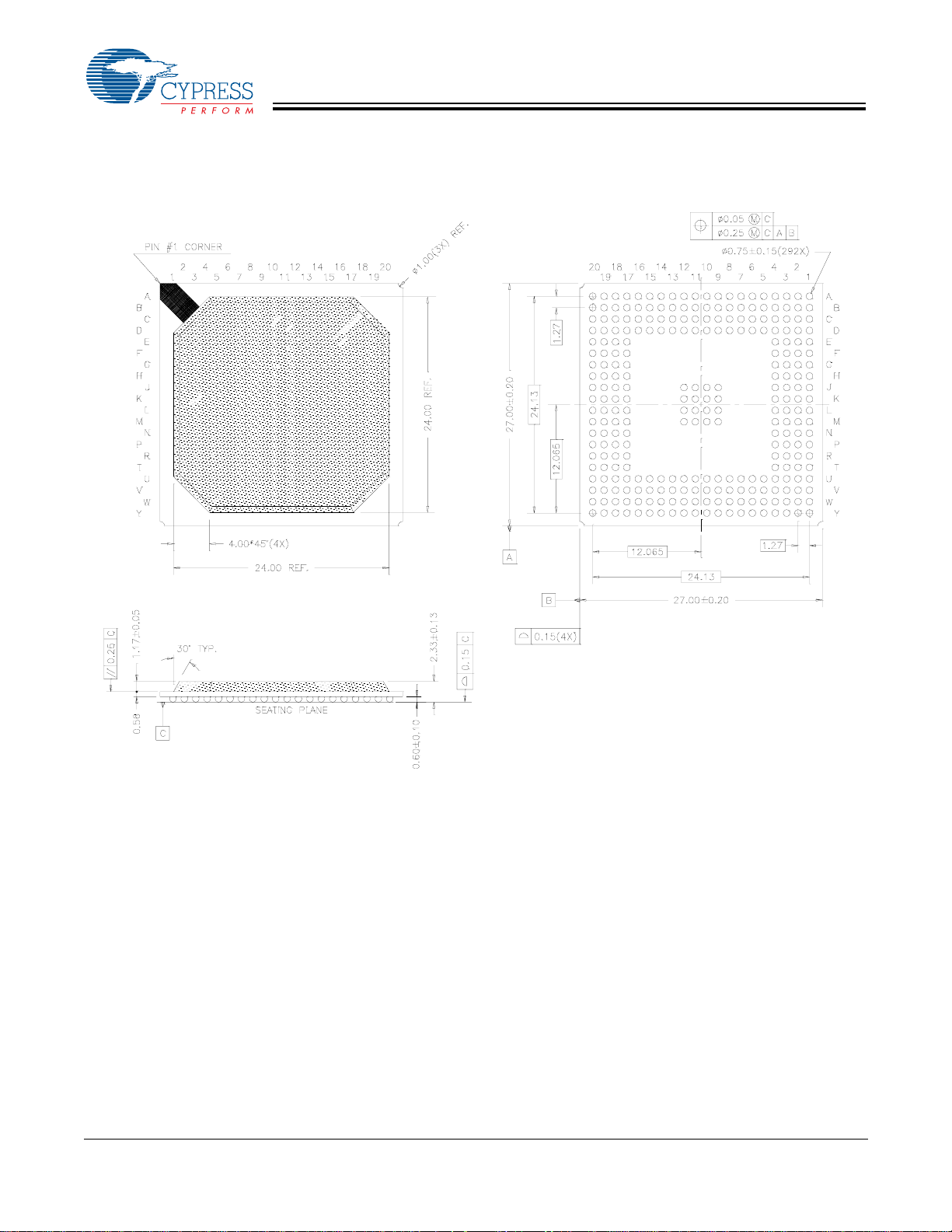
Package Diagram
272-Lead PBGA (27 x 27 x 2.33 mm) BG272
CY7C0430BV
CY7C0430CV
51-85130-*A
QuadPort is a trademark of Cypress Semiconductor Corporation. All product and company names mentioned in this document
are the trademarks of their respective holders.
Document #: 38-06027 Rev. *B Page 36 of 37
© Cypress Semiconductor Corporation, 2006. The information contained herein is subject to change without notice. Cypress Semiconductor Corporation assumes no responsibility for the use
of any circuitry other than circuitry embodied in a Cypress product. Nor does it convey or imply any license under patent or other rights. Cypress products are not warranted nor intended to be
used for medical, life support, life saving, critical control or safety applications, unless pursuant to an express written agreement with Cypress. Furthermore, Cypress does not authorize its
products for use as critical components in life-support systems where a malfunction or failure may reasonably be expected to result in significant injury to the user. The inclusion of Cypress
products in life-support systems application implies that the manufacturer assumes all risk of such use and in doing so indemnifies Cypress against all charges.
[+] Feedback
Page 37
Document History Page
Document Title: CY7C0430BV, CY7C0430CV 10 Gb/s 3.3V QuadPort DSE Family
Document Number: 38-06027
REV. ECN NO.
** 109906 09/10/01 SZV Change from Spec number: 38-01052 to 38-06027
*A 115042 05/23/02 FSG Remove Preliminary, TM from DSE
*B 464083 SEE ECN YDT
Issue
Date
Orig. of
Change Description of Change
Change RUNBIST to CYBIST
Updated ISB values
Added notes 7 and 9
Increased commercial prime bin to 135 MHz
Part numbers updated to reflect the recent die revisions
Removed 1/2M and 1/4M parts
Changed title of data sheet
CY7C0430BV
CY7C0430CV
Document #: 38-06027 Rev. *B Page 37 of 37
[+] Feedback
 Loading...