

Page 1
CY7C027V/027VN/027AV/028V
CY7C037V/037AV/038V
3.3V 32K/64K x 16/18 Dual-Port Static
RAM
Features
R/W
L
CE
0L
CE
1L
OE
L
I/O
8/9L
–I/O
15/17L
I/O
Control
Address
Decode
A
0L–A14/15L
CE
L
OE
L
R/W
L
BUSY
L
I/O
Control
CE
L
Interrupt
Semaphore
Arbitration
SEM
L
INT
L
M/S
UB
L
LB
L
I/O0L–I/O
7/8L
R/W
R
CE
0R
CE
1R
OE
R
I/O
8/9L
–I/O
15/17R
CE
R
UB
R
LB
R
I/O0L–I/O
7/8R
UB
L
LB
L
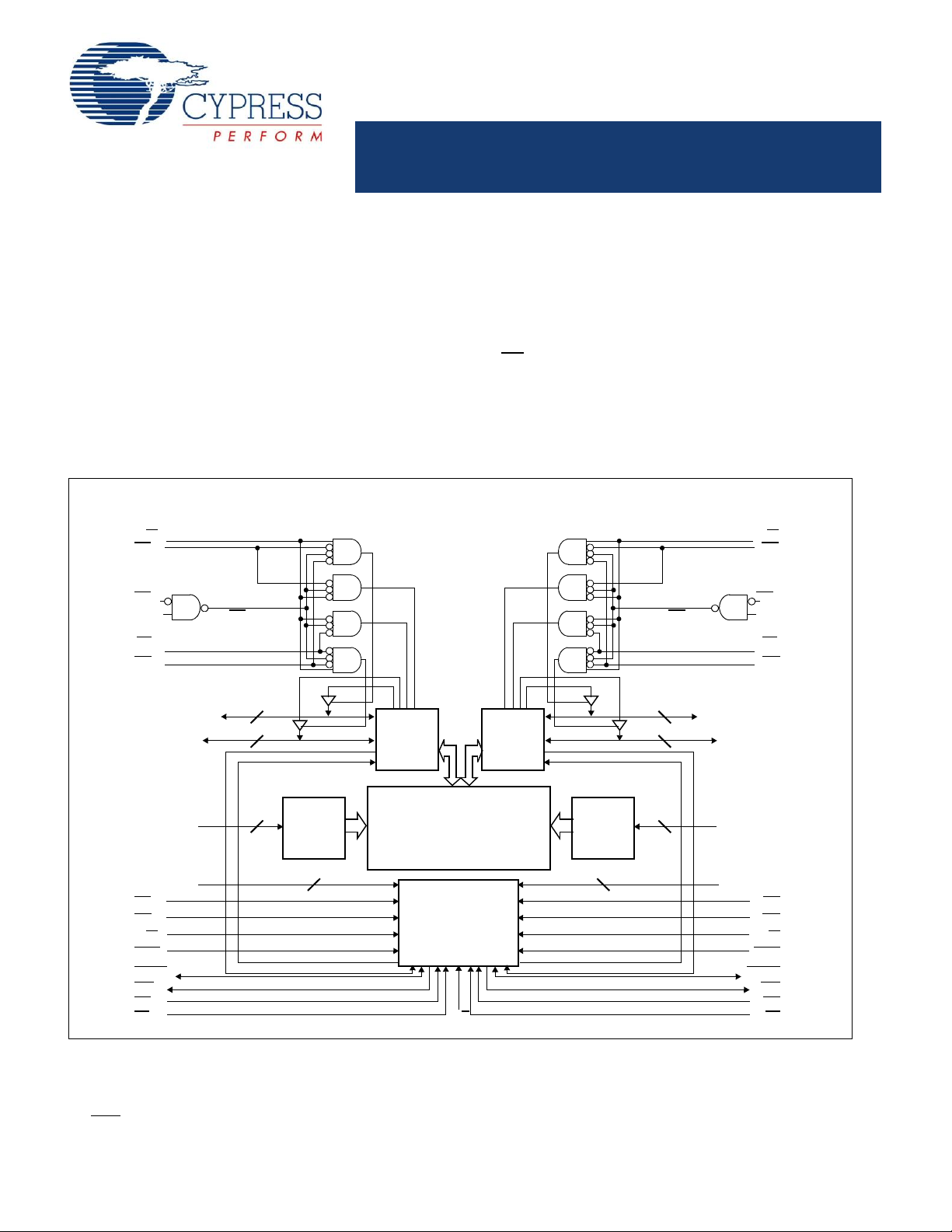
Logic Block Diagram
A0L–A
14/15L
True Dual-Ported
RAM Array
A0R–A
14/15R
CE
R
OE
R
R/W
R
BUSY
R
SEM
R
INT
R
UB
R
LB
R
Address
Decode
A
0R–A14/15R
[3]
[3]
[4]
[4]
[5]
[5]
[6]
[6]
[5] [5]
15/16
8/9
8/9
15/16
8/9
8/9
15/16 15/16
■
True Dual-Ported memory cells which allow
simultaneous access of the same memory location
■
32K x 16 organization (CY7C027V/027VN/027AV
■
64K x 16 organization (CY7C028V)
■
32K x 18 organization (CY7C037V/037AV
■
64K x 18 organization (CY7C038V)
■
0.35 micron CMOS for optimum speed and power
■
High speed access: 15, 20, and 25 ns
■
Low operating power
■
Active: ICC = 115 mA (typical)
■
Standby: I
= 10 μA (typical)
SB3
[2]
)
■
Fully asynchronous operation
■
Automatic power down
■
Expandable data bus to 32/36 bits or more using Master/Slave
[1]
)
chip select when using more than one device
■
On-chip arbitration logic
■
Semaphores included to permit software handshaking
between ports
■
INT flag for port-to-port communication
■
Separate upper-byte and lower-byte control
■
Dual chip enables
■
Pin select for Master or Slave
■
Commercial and Industrial temperature ranges
■
100-pin Pb-free TQFP and 100-pin TQFP
Notes
1. CY7C027V, CY7C027VN and CY7 C027AV are functionally identical.
2. CY7C037V and CY7C037AV are functionally identical.
–I/O15 for x16 devices; I/O9–I/O17 for x18 devices.
3. I/O
8
4. I/O
–I/O7 for x16 devices; I/O0–I/O8 for x18 devices.
0
5. A
0–A14
6. BUSY
Cypress Semiconductor Corporation • 198 Champion Court • San Jose,CA 95134-1709 • 408-943-2600
Document #: 38-06078 Rev. *B Revised December 09, 2008
for 32K; A0–A15 for 64K devices.
is an output in master mode and an input in slave mode.
[+] Feedback
Page 2
CY7C027V/027VN/027AV/028V
CY7C037V/037AV/038V
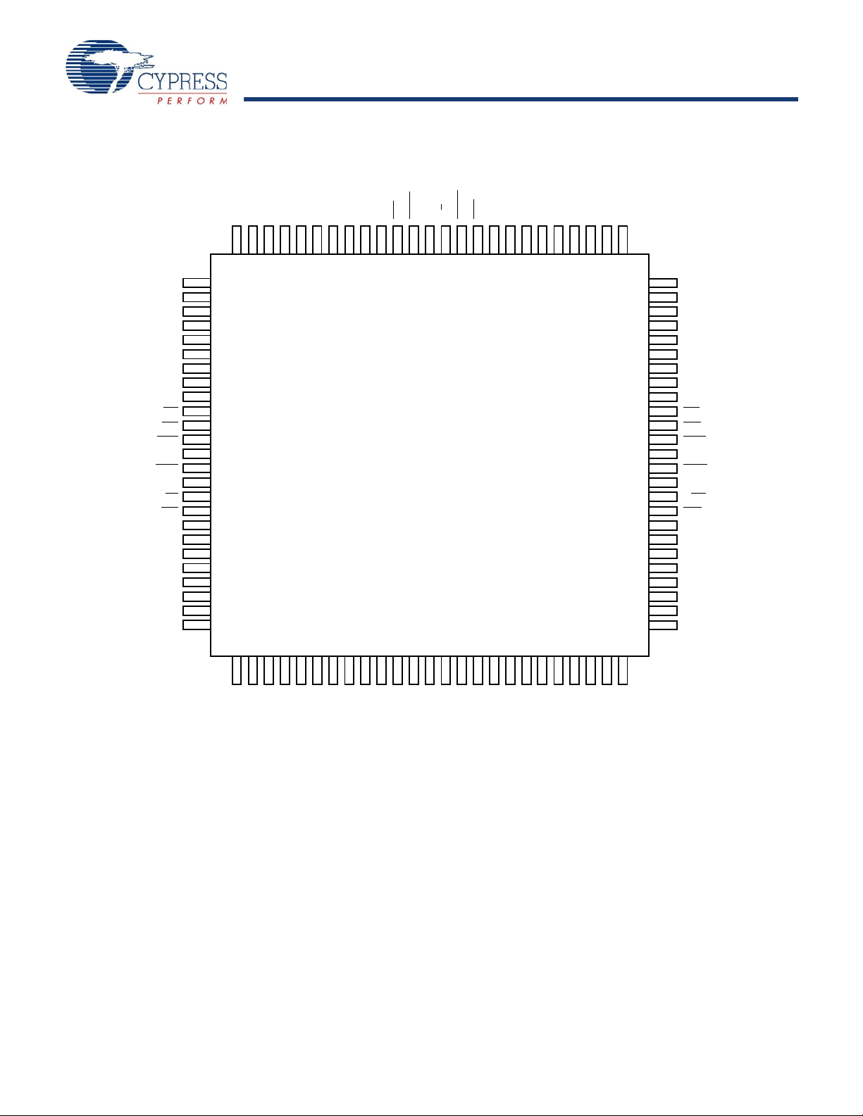
Pin Configurations
1
3
2
92 91 90 848587 868889 83 82 81 7678 77798093949596979899100
59
60
61
67
66
64
65
63
62
68
69
70
75
73
74
72
71
A9R
A10R
A11R
A12R
A13R
A14R
UBR
NC
LBR
CE1R
SEMR
OER
GND
NC
A15R
GND
R/WR
GND
I/O15R
I/O14R
I/O13R
I/O12R
I/O11R
I/O10R
CE0R
58
57
56
55
54
53
52
51
CY7C027V/027VN/027AV (32K x 16)
A9L
A10L
A11L
A12L
A13L
A14L
UBL
NC
LBL
CE1L
SEML
OEL
GND
NC
A15L
VCC
R/WL
GND
I/O15L
I/O14L
I/O13L
I/O12L
I/O11L
I/O10L
CE0L
17
16
15
9
10
12
11
13
14
8
7
6
4
5
18
19
20
21
22
23
24
25
A8L
A7L
A6L
A5L
A4L
A3L
INTL
A1L
NC
GND
M/S
A0R
A1R
A0L
A2L
BUSYR
INTR
A2R
A3R
A4R
A5R
A6R
A7R
A8R
BUSYL
34 35 36 424139 403837 43 44 45 5048 494746
NC
I/O9R
I/O8R
I/O7R
VCC
I/O6R
I/01R
I/O4R
I/O2R
GND
I/O0L
I/O2L
I/O3L
I/O3R
I/O5R
I/O1L
GND
I/O4L
I/O5L
I/O6L
I/O7L
VCC
I/O8L
I/O9L
I/O0R
3332313029282726
CY7C028V (64K x 16)
[1]
[1]
Note
1. This pin is NC for CY7C027V/027VN/027AV.
Figure 1. 100-Pin TQFP (Top View)
Document #: 38-06078 Rev. *B Page 2 of 18
[+] Feedback
Page 3
CY7C027V/027VN/027AV/028V
CY7C037V/037AV/038V
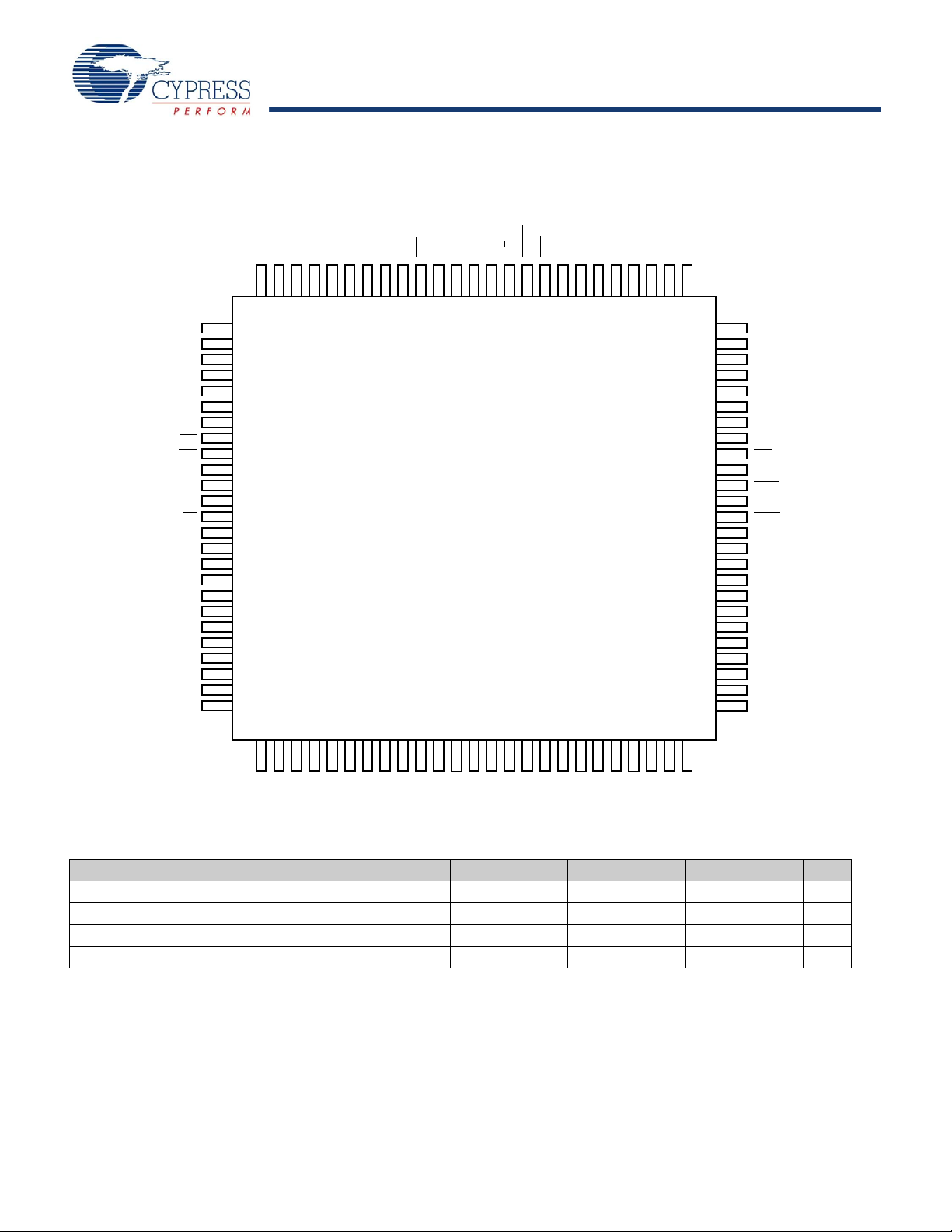
Pin Configurations
1
3
2
92 91 90 848587 868889 83 82 81 7678 77798093949596979899100
59
60
61
67
66
64
65
63
62
68
69
70
75
73
74
72
71
A8R
A9R
A10R
A11R
A12R
A13R
CE0R
A15R
UBR
SEMR
R/WR
GND
I/O17R
LBR
A14R
GND
OER
GND
I/O16R
I/O15R
I/O14R
I/O13R
I/O12R
I/O11R
CE1R
58
57
56
55
54
53
52
51
CY7C037V/037AV (32K x 18)
A9L
A10L
A11L
A12L
A13L
A14L
CE1L
LBL
CE0L
R/WL
OEL
I/O17L
I/O16L
UBL
A15L
VCC
GND
GND
I/O15L
I/O14L
I/O13L
I/O12L
I/O11L
I/O10L
SEML
17
16
15
9
10
12
11
13
14
8
7
6
4
5
18
19
20
21
22
23
24
25
A8L
A7L
A6L
A5L
A4L
A3L
BUSYL
A1L
INTL
GND
VCC
INTR
A0R
A0L
A2L
M/S
BUSYR
A1R
A2R
A3R
A4R
A5R
A6R
A7R
GND
34 35 36 424139 403837 43 44 45 5048 494746
I/O10R
I/O9R
I/O8R
I/O7R
VCC
I/O6R
I/01R
I/O4R
I/O2R
GND
I/O0L
I/O2L
I/O3L
I/O3R
I/O5R
I/O1L
GND
I/O4L
I/O5L
I/O6L
I/O7L
VCC
I/O8L
I/O9L
I/O0R
3332313029282726
CY7C038V (64K x 18)
[2]
[2]
Note
2. This pin is NC for CY7C037V/037AV.
(continued)
Figure 2. 100-Pin TQFP (Top View)
Selection Guide
Maximum Access Time 15 20 25 ns
Typical Operating Current 125 120 115 mA
Typical Standby Current for I
Typical Standby Current for I
Parameter -15 -20 -25 Unit
(Both ports TTL level) 35 35 30 mA
SB1
(Both ports CMOS level) 10 μA10 μA10 μA μA
SB3
Document #: 38-06078 Rev. *B Page 3 of 18
[+] Feedback
Page 4
CY7C027V/027VN/027AV/028V
CY7C037V/037AV/038V
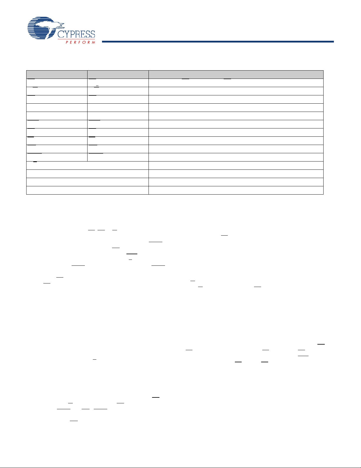
Pin Definitions
Left Port Right Port Description
CE
, CE
0L
1L
R/W
L
OE
L
A
0L–A15L
I/O0L–I/O
SEM
UB
LB
INT
BUSY
17L
SEM
L
L
L
L
L
M/S
V
CC
GND Ground
NC No Connect
CE0R, CE
R/W
R
OE
R
A0R–A
15R
I/O0R–I/O
R
UB
R
LB
R
INT
R
BUSY
R
1R
17R
Chip Enable (CE is LOW when CE0 ≤ VIL and CE1 ≥ VIH)
Read/Write Enable
Output Enable
Address (A0–A14 for 32K; A0–A15 for 64K devices)
Data Bus Input/Output (I/O0–I/O15 for x16 devices; I/O0–I/O17 for x18)
Semaphore Enable
Upper Byte Select (I/O8–I/O15 for x16 devices; I/O9–I/O17 for x18 devices)
Lower Byte Select (I/O0–I/O7 for x16 devices; I/O0–I/O8 for x18 devices)
Interrupt Flag
Busy Flag
Master or Slave Select
Power
Architecture
The CY7C027V/027VN/027AV/028V and
CY7037V/037AV/038V consist of an array of 32K and 64K words
of 16 and 18 bits each of dual-port RAM cells, I/O and address
lines, and control signals (CE
, OE, R/W). These control pins permit
independent access for reads or writes to any location in memory. To
handle simultaneous writes/reads to the same l ocatio n, a BUSY pin is
provided on each port. Two interrupt (INT
port-to-port communication. Two semaphore (SEM
used for allocating shared resources. With the M/S
function as a master (BUSY
pins are outputs) or as a slave (BUSY pins
) pins can be utilized for
) control pins are
pin, the devices can
are inputs). The devices also have an automatic power down feature
controlled by CE. Each port is provided with its own output enable
control (OE
), which allows data to be read from the d evice.
Functional Description
The CY7C027V/027VN/027AV/028V and
CY7037V/037AV/038V are low power CMOS 32K, 64K x 16/18
dual-port static RAMs. V arious arbitration schemes are included
on the devices to handle situations when multiple processors
access the same piece of data. Two ports are provided, permitting independent, asynchronous access for read s and writes to
any location in memory. The devices can be utilized as
stand-alone 16/18-bit dual-port static RAMs or multiple devices
can be combined to function as a 32/36-bit or wider master/slave
dual-port static RAM. An M/S
32/36-bit or wider memory applications without the need for separate master and slave devices or additional discrete logic. Application areas include interprocessor/multiprocessor designs,
communications status buffering, and dual-port video/graphics
memory.
Each port has independent control pins: chip enable (CE
or write enable (R/ W
on each port (BUSY
), and output enable (OE). T wo flags are provided
and INT). BUSY signals that the port is trying to
access the same location currently being accessed by the othe r port.
The interrupt flag (INT
) permits communication between ports or
pin is provided for implementing
), read
systems by means of a mail box. The semaphores are used to pass a
flag, or token, from one port to the other to indi cate that a shared
resource is in use. The semaphore logic is comprised of eight shared
latches. Only one side can control the latch (semaphore) at any time.
Control of a semaphore indicates that a shared re sou rce i s in use . An
automatic power down feature is controlle d independently on each port
by a chip select (CE
) pin.
The CY7C027V/027VN/027AV/028V and
CY7037V/037AV/038V are available in 100-pin Thin Quad Plastic Flatpacks (TQFP).
Write Operation
Data must be set up for a duration of tSD before the rising edge of
to guarantee a valid write. A write operation is controlled by either
R/W
the R/W
pin (see Figure 7 ) or the CE pin (see Figure8). Required inputs
for non-contention operations are summarized in Table 1.
If a location is being written to by one port and the opposite port
attempts to read that location, a port-to-port flowthrough delay
must occur before the data is read on the output; otherwise the
data read is not deterministic. Data is valid on the port t
the data is presented on the other port.
DDD
after
Read Operation
When reading the device, the user must assert both the OE an d
pins. Data is available t
CE
the user wishes to access a semaphore flag, then the SEM
asserted instead of the CE
after CE or t
ACE
after OE is asserted. If
DOE
pin must be
pin, and OE must also be asserted.
Interrupts
The upper two memory locations may be used for message
passing. The highest memory location (7FFF for the
CY7C027V/027VN/027AV/37V, FFFF for the CY7C028V/38V) is
the mailbox for the right port and the second-highest memory
location (7FFE for the CY7C027V/027VN/027AV/037V/037AV,
FFFE for the CY7C028V/38V) is the mailbox for the left port.
When one port writes to the other port’s mailbox, an interrupt is
Document #: 38-06078 Rev. *B Page 4 of 18
[+] Feedback
Page 5

CY7C027V/027VN/027AV/028V
CY7C037V/037AV/038V
generated to the owner. The interrupt is reset when the owner
reads the contents of the mailbox. The message is user defined.
Each port can read the other port’s mailbox without resetting the
interrupt. The active state of the busy signal (to a port) prevents
the port from setting the interrupt to the winning port. Also, an
active busy to a port prevents that port from reading its own
mailbox and, thus, resetting the interrupt to it.
If an application does not require message passing, do not
connect the interrupt pin to the processor’s interrupt request
input pin.
The operation of the interrupts and their interaction with Busy are
summarized in Table 2.
Busy
The CY7C027V/027VN/027AV/028V and
CY7037V/037AV/038V provide on-chip arbitration to resolve
simultaneous memory location access (contention). If both ports’
CE
s are asserted and an address match occurs within tPS of each other,
the busy logic determines which port has access. If t
port definitely gains permission to the location, but it is not predictable
which port gets that permission. BUSY is asserted t
match or t
after CE is taken LOW.
BLC
is violated, one
PS
after an address
BLA
Master/Slave
A M/S pin is provided to expand the word width by configuring the
device as either a master or a sl ave. The BUSY
connected to the BUSY
input of the slave. This allows the device to
output of the master is
interface to a master device with no external components. Writing to
slave devices must be delayed until after the BUSY
or t
(t
BLC
a contention situation. When tied HIGH, the M/S
), otherwise, the slave chip may begin a write cycle during
BLA
to be used as a master and, therefore, the BUSY
input has settled
pin allows the device
line is an output. BUSY
can then be used to send the arbitration outcome to a slave.
Semaphore Operation
The CY7C027V/027VN/027AV/028V and
CY7037V/037AV/038V provide eight semaphore latches, which
are separate from the dual-port memory locations. Semaphores
are used to reserve resources that are shared be tween th e two
ports.The state of the semaphore indicates that a resource is in
use. For example, if the left port wants to request a given
resource, it sets a latch by writing a zero to a semaphore location.
The left port then verifies its success in setting the latch by
reading it. After writing to the semaphore, SEM
deasserted for t
semaphore value is available t
semaphore write. If the left port was successful (reads a zero), it
before attempting to read the semaphore. The
SOP
SWRD
+ t
after the rising edge of the
DOE
or OE must be
assumes control of the shared resource, otherwise (reads a one) it
assumes the right port has control and continues to poll the semaphore.
When the right side has relinquished control of the semaph ore (by
writing a one), the left side succeeds in gaining control of the
semaphore. If the left side no longer requires the semap hore, a one i s
written to cancel its request.
Semaphores are accessed by asserting SEM
functions as a chip select for the semaphore latches (CE
HIGH during SEM
and R/W are used in the same manner as a normal memory access.
LOW). A
represents the semaphore address. OE
0–2
LOW. The SEM pin
must remain
When writing or reading a semaphore, the other address pins have no
effect.
When writing to the semaphore, only I/O
to the left port of an available semaphore, a one appears at the same
is used. If a zero is written
0
semaphore address on the right port . That semaphore can now only be
modified by the side showing zero (the left port in this case). If the left
port now relinquishes control by writing a one to the semaphore, the
semaphore is set to one for both sides. However, if the right port had
requested the semaphore (written a zero) while th e left port had control,
the right port would immediately own the semaphore as so on as the left
port released it. Table 3 shows sample semaphore operations.
When reading a semaphore, all sixteen/eighteen data lines
output the semaphore value. The read value is latched in an
output register to prevent the semaphore from changing state
during a write from the other port. If both ports attempt to access
the semaphore within t
obtained by one side or the other, but there is no guarantee which side
of each other , the semaphore is definitely
SPS
controls the semaphore.
Document #: 38-06078 Rev. *B Page 5 of 18
[+] Feedback
Page 6
CY7C027V/027VN/027AV/028V
CY7C037V/037AV/038V
Maximum Ratings
Exceeding maximum ratings may shorten the useful life of the
device. User guidelines are not tested .
°
Storage Temperature .................................–65
Ambient Temperature with
Power Applied ............................................–55
Supply Voltage to Ground Potential................–0.5V to +4.6V
DC Voltage Applied to
Outputs in High-Z State...........................–0.5V to VCC+0.5V
C to +150°C
°
C to +125°C
DC Input Voltage
[2]
..................................–0.5V to VCC+0.5V
Output Current into Outputs (LOW).............................20 mA
Static Discharge Voltage.......................................... > 1100V
Latch-up Current.................................................... > 200 mA
Operating Range
Range
Commercial 0°C to +70°C 3.3V ± 300 mV
Industrial
[3]
Ambient
Temperature V
CC
–40°C to +85°C 3.3V ± 300 mV
Electrical Characteristics
Over the Operating Range
Parameter Description
V
V
V
V
I
IX
I
OZ
I
CC
I
SB1
I
SB2
I
SB3
I
SB4
OH
OL
IH
IL
Output HIGH Voltage
(V
=Min., IOH= –4.0 mA)
CC
Output LOW Voltage (VCC=Min., IOH= +4.0 mA) 0.4 0.4 0.4 V
Input HIGH Voltage 2.2 2.2 2.2 V
Input LOW Voltage 0.8 0.8 0.8 V
Input Leakage Current −55−55−55μA
Output Leakage Current –10 10 –10 10 –10 10 μA
Operating Current (VCC=Max. I
mA) Outputs Disabled
Standby Current (Both Ports TTL
Level) CE
& CER ≥ VIH, f=f
L
Standby Current (One Port TTL Level)
CE
| CER ≥ VIH, f=f
L
MAX
Standby Current (Both Ports CMOS
Level) CE
& CER ≥ VCC−0.2V, f=0
L
Standby Current (One Port CMOS Lev-
| CER ≥ VIH, f=f
el) CE
L
MAX
MAX
[4]
OUT
CY7C027V/027VN/027AV/028V/CY7C037V/037AV/038V
Min Typ Max Min Typ Max Min Typ Max
2.4 2.4 2.4 V
=0
Com’l. 125 185 120 175 115 165 mA
[3]
Ind.
140 195 mA
Com’l. 35 50 35 45 30 40 mA
[3]
Ind.
45 55 mA
Com’l. 80 120 75 110 65 95 mA
[3]
Ind.
85 120 mA
Com’l. 10 250 10 250 10 250 μA
Ind.
[3]
10 250 μA
Com’l. 75 105 70 95 60 80 mA
[3]
Ind.
80 105 mA
Unit-15 -20 -25
Capacitance
[5]
Parameter Description Test Conditions Max Unit
C
IN
C
OUT
Notes
2. Pulse width < 20 ns.
3. Industrial parts are available in CY7C028V and CY7C038V only.
4. f
= 1/tRC = All inputs cycling at f = 1/tRC (except output enable). f = 0 means no addr ess or control line s change. This appli es only to input s at CMOS level st andby I
MAX
5. Tested initially and after any design or process changes that may affect these parameters.
Document #: 38-06078 Rev. *B Page 6 of 18
Input Capacitance TA = 25°C, f = 1 MHz,
V
= 3.3V
Output Capacitance 10 pF
CC
10 pF
SB3
.
[+] Feedback
Page 7

CY7C027V/027VN/027AV/028V
CY7C037V/037AV/038V
Figure 3. AC Test Loads and Waveforms
3.0V
GND
90%
90%
10%
3ns
3
ns
10%
ALL INPUTPULSES
(a) Normal Load (Load
1)
R1 = 590Ω
3.3V
OUTPUT
R2 = 435Ω
C= 30
pF
V
TH
=1.4V
OUTPUT
C= 30 pF
(b) Thévenin Equivalent (Load 1)
(c)Three-State Delay(Load 2)
R1 = 590Ω
R2 = 435Ω
3.3V
OUTPUT
C= 5pF
R
TH
= 250Ω
≤
≤
including scope and jig)
(Used for t
LZ
, tHZ, t
HZWE
, & t
LZWE
Switching Characteristics
Parameter Description
Read Cycle
t
RC
t
AA
t
OHA
[7]
t
ACE
t
DOE
[8, 9, 10]
t
LZOE
[8, 9, 10]
t
HZOE
[8, 9, 10]
t
LZCE
[8, 9, 10]
t
HZCE
[10]
t
PU
[10]
t
PD
[7]
t
ABE
Write Cycle
t
WC
[7]
t
SCE
t
AW
t
HA
[7]
t
SA
t
PWE
t
SD
Notes
6. T est conditions assume signal transition ti me of 3 ns or less, timing refer ence levels of 1.5V, input pulse levels of 0 to 3.0V, and output loading of the specified I
and 30 pF load capacitance.
7. To access RAM, CE
8. At any given temperature and voltage condition for any given device, t
9. Test conditions used are Load 2.
10.This parameter is guaranteed by design, but it is not production tested. For information on port-to-port delay through RAM cells from writing port to reading port,
refer to Figure 11.
Over the Operating Range
[6]
CY7C027V/027VN/027AV/028V/
CY7C037V/037AV/038V
-15 -20 -25
Min Max Min Max Min Max
Read Cycle Time 15 20 25 ns
Address to Data Valid 15 20 25 ns
Output Hold From Address Change 3 3 3 ns
CE LOW to Data Valid 15 20 25 ns
OE LOW to Data Valid 10 12 13 ns
OE LOW to Low Z 3 3 3 ns
OE HIGH to High Z 10 12 15 ns
CE LOW to Low Z 3 3 3 ns
CE HIGH to High Z 10 12 15 ns
CE LOW to Power Up 0 0 0 ns
CE HIGH to Power Down 15 20 25 ns
Byte Enable Access Time 15 20 25 ns
Write Cycle Time 15 20 25 ns
CE LOW to Write End 12 16 20 ns
Address Valid to Write End 12 16 20 ns
Address Hold From Write End 0 0 0 ns
Address Setup to Write Start 0 0 0 ns
Write Pulse Width 12 17 22 ns
Data Setup to Write End 10 12 15 ns
=L, UB=L, SEM=H. T o access semaphore, CE=H and SEM=L. Either condition must be valid for the entire t
is less than t
HZCE
LZCE
and t
is less than t
HZOE
LZOE
time.
SCE
.
Unit
OI/IOH
Document #: 38-06078 Rev. *B Page 7 of 18
[+] Feedback
Page 8

CY7C027V/027VN/027AV/028V
CY7C037V/037AV/038V
Switching Characteristics
Data Retention Mode
3.0V
3.0V
V
CC
> 2.0V
V
CC
to VCC– 0.2V
V
CC
CE
t
RC
V
IH
Notes
11.For information on port-to-port delay through RAM cells from writing port to reading port, refer to Figure11 waveform.
12.Test conditions used are Load 1.
13.t
BDD
is a calculated parameter and is the grea ter of t
WDD–tPWE
(actual) or t
DDD–tSD
(actual).
14.CE
= VCC, Vin = GND to VCC, TA = 25° C. This parameter is guaranteed but not tested.
Over the Operating Range
Parameter Description
t
HD
[9, 10]
t
HZWE
[9 ,10]
t
LZWE
[36]
t
WDD
[36]
t
DDD
Busy Timing
t
BLA
t
BHA
t
BLC
t
BHC
t
PS
t
WB
t
WH
[13]
t
BDD
Interrupt Timing
t
INS
t
INR
Data Hold From Write End 0 0 0 ns
R/W LOW to High Z 10 12 15 ns
R/W HIGH to Low Z 3 3 3 ns
Write Pulse to Data Delay 30 40 50 ns
Write Data Valid to Read Data Valid 25 30 35 ns
[11]
BUSY LOW from Address Match 15 20 20 ns
BUSY HIGH from Address Mismatch 15 20 20 ns
BUSY LOW from CE LOW 15 20 20 ns
BUSY HIGH from CE HIGH 15 16 17 ns
Port Setup for Priority 5 5 5 ns
R/W HIGH after BUSY (Slave) 0 0 0 ns
R/W HIGH after BUSY H I G H ( S l a v e ) 13 15 17 ns
BUSY HIGH to Data Valid 15 20 25 ns
[11]
INT Set Time 15 20 20 ns
INT Reset Time 15 20 20 ns
Semaphore Timing
t
SOP
t
SWRD
t
SPS
t
SAA
SEM Flag Update Pulse (OE or SEM)101012ns
SEM Flag Write to Read Time 5 5 5 ns
SEM Flag Contention Window 5 5 5 ns
SEM Address Access Time 15 20 25 ns
Data Retention Mode
The CY7C027V/027VN/027AV/028V and
CY7037V/037AV/038V are designed with battery backup in
mind. Data retention voltage and supply current are guaranteed
over temperature. The following rules ensure data retention:
1. Chip enable (CE) must be held HIGH during data retention, within
to VCC – 0.2V .
V
CC
must be kept between VCC – 0.2V and 70% of VCC during
2. CE
the power up and power down transitions.
3. The RAM can begin opera tion >t
mum operating voltage (3.0 volt s).
after VCC reaches the mini-
RC
[6]
(continued)
CY7C027V/027VN/027AV/028V/
CY7C037V/037AV/038V
-15 -20 -25
Min Max Min Max Min Max
Timing
Parameter Test Conditions
ICC
DR1
At VCCDR = 2V 50 μA
[14]
Unit
Max Unit
Document #: 38-06078 Rev. *B Page 8 of 18
[+] Feedback
Page 9

CY7C027V/027VN/027AV/028V
CY7C037V/037AV/038V
Switching Waveforms
t
RC
t
AA
t
OHA
DATA VALIDPREVIOUS DATA VALID
DATA OUT
ADDRESS
t
OHA
Figure 4. Read Cycle No. 1 (Either Port Address Access)
[15, 16, 17]
t
ACE
t
LZOE
t
DOE
t
HZOE
t
HZCE
DATA VALID
t
LZCE
t
PU
t
PD
I
SB
I
CC
DATA OUT
OE
CE and
LB
or UB
CURRENT
Figure 5. Read Cycle No. 2 (Either Port CE/OE Access)
[15, 18, 19]
UB or LB
DATAOUT
t
RC
ADDRESS
t
AA
t
OHA
CE
t
LZCE
t
ABE
t
HZCE
t
HZCE
t
ACE
t
LZCE
Figure 6. Read Cycle No. 3 (Either Port)
[15, 17, 18, 19]
Notes
15.R/W
is HIGH for read cycles.
16.Device is continuously selected CE = VIL and UB or LB = VIL. This waveform cannot be used for semaphor e reads.
= VIL.
17.OE
18.Address valid prior to or coincident with CE
19.To access RAM, CE = VIL, UB or LB = VIL, SEM = VIH. T o access semaphore, CE = VIH, SEM = VIL.
Document #: 38-06078 Rev. *B Page 9 of 18
transition LOW.
[+] Feedback
Page 10

CY7C027V/027VN/027AV/028V
CY7C037V/037AV/038V
Switching Waveforms
t
AW
t
WC
t
PWE
t
HD
t
SD
t
HA
CE
R/W
OE
DATAOUT
DATA IN
ADDRESS
t
HZOE
t
SA
t
HZWE
t
LZWE
Figure 7. Write Cycle No. 1: R/W Controlled Timing
[20, 21, 22, 23]
[26]
[26]
[23]
[24,25]
NOTE 27
NOTE 27
t
AW
t
WC
t
SCE
t
HD
t
SD
t
HA
CE
R/W
DATA IN
ADDRESS
t
SA
Figure 8. Write Cycle No. 2: CE Controlled Timing
[20, 21, 22, 28]
[24,25]
(continued)
Notes
20.R/W must be HIGH during all address transitions.
21.A write occurs during the overlap (t
is measured from the earlier of CE or R/W or (SEM or R/W) going HIGH at the end of write cycle.
22.t
HA
is LOW during a R/W controlled write cycle, the write pulse width must be the larger of t
23.If OE
the bus for the required t
24.To access RAM, CE
25.To access upper byte, CE
T o access lower byte, CE
26.Transition is measured ±500 mV from steady state with a 5 p F load (includi ng scope and ji g). This p arameter is sample d and not 100% te sted.
27.During this period, the I/O pins are in the output state, and input signals must not be applied.
28.If the CE
or SEM LOW transition occurs simultaneously with or after the R/W LOW transition, the outputs remain in the high impedance state.
. If OE is HIGH during an R/W controlled write cycle, this requirement does not apply and the write pulse can be as short as the specified t
SD
= VIL, SEM = VIH.
= VIL, UB = VIL, SEM = VIH.
= VIL, LB = VIL, SEM = VIH.
SCE
or t
Document #: 38-06078 Rev. *B Page 10 of 18
) of a LOW CE or SEM and a LOW UB or LB.
PWE
or (t
PWE
HZWE
+ tSD) to allow the I/O drivers to turn off and data to be placed on
PWE
.
[+] Feedback
Page 11

CY7C027V/027VN/027AV/028V
CY7C037V/037AV/038V
Switching Waveforms
t
SOP
t
SAA
VALID ADRESS VALID ADRESS
t
HD
DATAINVALID
DATA
OUT
VALID
t
OHA
t
AW
t
HA
t
ACE
t
SOP
t
SCE
t
SD
t
SA
t
PWE
t
SWRD
t
DOE
WRITE CYCLE READ CYCLE
OE
R/W
I/O
0
SEM
0–A2
Figure 9. Semaphore Read After Write Timing, Either Side
[29]
A
MATCH
t
SPS
A0L–A
2L
MATCH
R/W
L
SEM
L
A0R–A
2R
R/W
R
SEM
R
Figure 10. Timing Diagram of Semaphore Contention
[30, 31, 32]
(continued)
Notes
29.CE
= HIGH for the duration of the above timing (both write and read cycle).
30.I/O
= I/O0L = LOW (request semaphore); CER = CEL = HIGH.
0R
31.Semaphores are reset (available t o both ports) at cycle start.
is violated, the semaphore is definit ely obtain ed by one side or the o ther , but whi ch side get s the semaphore is u npredictable .
32.If t
SPS
Document #: 38-06078 Rev. *B Page 11 of 18
[+] Feedback
Page 12

CY7C027V/027VN/027AV/028V
CY7C037V/037AV/038V
Switching Waveforms
VALID
t
DDD
t
WDD
MATCH
MATCH
R/W
R
DATA IN
R
DATA
OUTL
t
WC
ADDRESS
R
t
PWE
VALID
t
SD
t
HD
ADDRESS
L
t
PS
t
BLA
t
BHA
t
BDD
BUSY
L
Figure 11. Timing Diagram of Read with BUSY (M/S=HIGH)
[33]
t
PWE
R/W
BUSY
t
WB
t
WH
Figure 12. Write Timing with Busy Input (M/S=LOW)
(continued)
Note
33.CE
= CER = LOW.
L
Document #: 38-06078 Rev. *B Page 12 of 18
[+] Feedback
Page 13

CY7C027V/027VN/027AV/028V
CY7C037V/037AV/038V
Switching Waveforms
ADDRESS MATCH
t
PS
t
BLC
t
BHC
ADDRESS MATCH
t
PS
t
BLC
t
BHC
CERValidFirst:
ADDRESS
L,R
BUSY
R
CE
L
CE
R
BUSY
L
CE
R
CE
L
ADDRESS
L,R
Figure 13. Busy Timing Diagram No. 1 (CE Arbitration)
[34]
CELValid First:
ADDRESS MATCH
t
PS
ADDRESS
L
BUSY
R
ADDRESS MISMATCH
t
RC
or t
WC
t
BLA
t
BHA
ADDRESS
R
ADDRESS MATCH ADDRESS MISMATCH
t
PS
ADDRESS
L
BUSY
L
tRCor t
WC
t
BLA
t
BHA
ADDRESS
R
Right Address Valid First:
Figure 14. Busy Timing Diagram No. 2 (Address Arbitration)
[34]
Left Address Valid First:
(continued)
Note
34.If t
is violated, the busy signal is asserted on one side or the ot her , but t here is no guaran tee to which side BUSY is asserted.
PS
Document #: 38-06078 Rev. *B Page 13 of 18
[+] Feedback
Page 14

CY7C027V/027VN/027AV/028V
CY7C037V/037AV/038V
Switching Waveforms
WRITE 7FFF (FFFF for CY7C028V/38V)
t
WC
Right Side Clears INTR:
t
HA
READ 7FFF
t
RC
t
INR
WRITE 7FFE (FFFE for CY7C028V/38V)
t
WC
Right Side Sets INT
L
:
Left Side Sets INTR:
Left SideClears INT
L
:
READ 7FFE
t
INR
t
RC
ADDRESS
R
CE
L
R/W
L
INT
L
OE
L
ADDRESS
R
R/W
R
CE
R
INT
L
ADDRESS
R
CE
R
R/W
R
INT
R
OE
R
ADDRESS
L
R/W
L
CE
L
INT
R
t
INS
t
HA
t
INS
(FFFF for CY7C028V/38V)
(FFFF for CY7C028V/38V)
[35]
[36]
[36]
[36]
[35]
[36]
(continued)
Figure 15. Interrupt Timing Diagrams
Notes
depends on which enable pin (CEL or R/WL) is deasserted first.
35.t
HA
or t
36.t
INS
Document #: 38-06078 Rev. *B Page 14 of 18
depends on which enable pin (CEL or R/WL) is asserted last.
INR
[+] Feedback
Page 15

CY7C027V/027VN/027AV/028V
CY7C037V/037AV/038V
Table 1. Non-Contending Read/Write
Inputs Outputs
CE R/W OE UB LB SEM I/O9–I/O
17
I/O0–I/O
8
Operation
H X X X X H High Z High Z Deselected: Power Down
X X X H H H High Z High Z Deselected: Power Down
L L X L H H Data In High Z Write to Upper Byte Only
L L X H L H High Z Data In Write to Lower Byte Only
L L X L L H Data In Data In Write to Both Bytes
L H L L H H Data Out High Z Read Upper Byte Only
L H L H L H High Z Data Out Read Lower Byte Only
L H L L L H Data Out Data Out Read Both Bytes
X X H X X X High Z High Z Outputs Disabled
H H L X X L Data Out Data Out Read Data in Semaphore Flag
X H L H H L Data Out Data Out Read Data in Semaphore Flag
H X X X L Data In Data In Write D
into Semaphore Flag
IN0
X X H H L Data In Data In Write D
into Semaphore Flag
IN0
L X X L X L Not Allowed
L X X X L L Not Allowed
Table 2. Interrupt Operation Example (assumes BUSY
=BUSYR=HIGH)
L
[37]
Left Port Right Port
Function R/WLCELOE
L
Set Right INTR Flag L L X 7FFF X X X X X L
Reset Right INTR FlagXXXXXXLL7FFFH
Set Left INTL Flag XXX X L
Reset Left INT
Flag X L L 7FFE H
L
A
0L–14L
INTLR/WRCE
[38]
[39]
LLX 7FFE X
XXX X X
OE
R
R
A
0R–14R
INT
[39]
R
[38]
Table 3. Semaphore Operation Example
Function I/O0–I/O
Left I/O0–I/O
17
Right Status
17
No action 1 1 Semaphore free
Left port writes 0 to semaphore 0 1 Left port has semaphore token
Right port writes 0 to semaphore 0 1 No change. Right side has no write access to semaphore
Left port writes 1 to semaphore 1 0 Right port obtains semaphore token
Left port writes 0 to semaphore 1 0 No change. Left port has no write access to semaphore
Right port writes 1 to semaphore 0 1 Left port obtains semaphore token
Left port writes 1 to semaphore 1 1 Semaphore free
Right port writes 0 to semaphore 1 0 Right port has semaphore token
Right port writes 1 to semaphore 1 1 Semaphore free
Left port writes 0 to semaphore 0 1 Left port has semaphore token
Left port writes 1 to semaphore 1 1 Semaphore free
Notes
37.A
38. If BUSY
39. If BUSY
and A
0L–15L
=L, then no change.
R
=L, then no change.
L
,FFFF/FFFE for the CY7C028V/038V .
0R–15R
Document #: 38-06078 Rev. *B Page 15 of 18
[+] Feedback
Page 16

CY7C027V/027VN/027AV/028V
CY7C037V/037AV/038V
Ordering Information
32K x16 3.3V Asynchronous Dual-Port SRAM
Speed
(ns) Ordering Code
15 CY7C027V-15AC A100 100-Pin Thin Quad Flat Pack Commercial
CY7C027V-15AXC A100 100-Pin Pb-Free Thin Quad Flat Pack Commercial
CY7C027VN-15AXC A100 100-Pin Pb-Free Thin Quad Flat Pack Commercial
20 CY7C027V-20AC A100 100-Pin Thin Quad Flat Pack Commercial
CY7C027V-20AXC A100 100-Pin Pb-Free Thin Quad Flat Pack Commercial
25 CY7C027V-25AC A100 100-Pin Thin Quad Flat Pack Commercial
CY7C027V-25AXC A100 100-Pin Pb-Free Thin Quad Flat Pack Commercial
CY7C027AV-25AXI A100 100-Pin Pb-Free Thin Quad Flat Pack Industrial
64K x16 3.3V Asynchronous Dual-Port SRAM
Speed
(ns) Ordering Code
15 CY7C028V-15AC A100 100-Pin Thin Quad Flat Pack Commercial
CY7C028V-15AXC A100 100-Pin Pb-Free Thin Quad Flat Pack Commercial
20 CY7C028V-20AC A100 100-Pin Thin Quad Flat Pack Commercial
CY7C028V-20AXC A100 100-Pin Pb-Free Thin Quad Flat Pack Commercial
CY7C028V-20AI A100 100-Pin Thin Quad Flat Pack Industrial
CY7C028V-20AXI A100 100-Pin Pb-F ree Thin Quad Flat Pack Industrial
25 CY7C028V-25AC A100 100-Pin Thin Quad Flat Pack Commercial
CY7C028V-25AXC A100 100-Pin Pb-Free Thin Quad Flat Pack Commercial
Package
Name Package Type
Package
Name Package Type
Operating
Range
Operating
Range
32K x18 3.3V Asynchronous Dual-Port SRAM
Speed
(ns) Ordering Code
15 CY7C037V-15AC A100 100-Pin Thin Quad Flat Pack Commercial
CY7C037V-15AXC A100 100-Pin Pb-Free Thin Quad Flat Pack Commercial
20 CY7C037V-20AC A100 100-Pin Thin Quad Flat Pack Commercial
CY7C037AV-20AXC A100 100-Pin Pb-Free Thin Quad Flat Pack Commercial
25 CY7C037V-25AC A100 100-Pin Thin Quad Flat Pack Commercial
CY7C037V-25AXC A100 100-Pin Pb-Free Thin Quad Flat Pack Commercial
Package
Name Package Type
64K x18 3.3V Asynchronous Dual-Port SRAM
Speed
(ns) Ordering Code
15 CY7C038V-15AC A100 100-Pin Thin Quad Flat Pack Commercial
CY7C038V-15AXC A100 100-Pin Pb-Free Thin Quad Flat Pack Commercial
20 CY7C038V-20AC A100 100-Pin Thin Quad Flat Pack Commercial
CY7C038V-20AXC A100 100-Pin Pb-Free Thin Quad Flat Pack Commercial
CY7C038V-20AI A100 100-Pin Thin Quad Flat Pack Industrial
CY7C038V-20AXI A100 100-Pin Pb-F ree Thin Quad Flat Pack Industrial
25 CY7C038V-25AC A100 100-Pin Thin Quad Flat Pack Commercial
CY7C038V-25AXC A100 100-Pin Pb-Free Thin Quad Flat Pack Commercial
Package
Name Package Type
Operating
Range
Operating
Range
Document #: 38-06078 Rev. *B Page 16 of 18
[+] Feedback
Page 17

CY7C027V/027VN/027AV/028V
CY7C037V/037AV/038V
Package Diagram
51-85048-*C
Figure 16. 100-Pin Pb-Free Thin Plastic Quad Flat Pack (TQFP) A100
Document #: 38-06078 Rev. *B Page 17 of 18
[+] Feedback
Page 18

CY7C027V/027VN/027AV/028V
CY7C037V/037AV/038V
Document History Page
Document Title: CY7C027V/027VN/027AV/CY7C028V/037V/037AV/038V 3.3V 32K/64K x 16/18 Dual Port Static RAM
Document Number: 38-06078
Rev. ECN No.
Orig. of
Change
Submission
Date
Description of Change
** 237626 YDT 6/30/04 Converted data sheet from old spec 38-00670 to conform with new data
sheet. Removed cross information from features section
*A 259110 JHX See ECN Added Pb-Free packaging information.
*B 2623540 VKN/PYRS 12/17/08 Added CY7C027VN, CY7C027AV and CY7C037AV parts
Updated Ordering information table
Sales, Solutions, and Legal Information
Worldwide Sales and Design Support
Cypress maintains a worldwide network of offices, solution centers, manufacturer’s representatives, and distributors. T o find the office
closest to you, visit us at cypress.com/sales.
Products
PSoC psoc.cypress.com
Clocks & Buffers clocks.cypress.com
Wireless wireless.cypress.com
Memories memory.cypress.com
Image Sensors image.cypress.com
PSoC Solutions
General psoc.cypress.com/solutions
Low Power/Low Voltage psoc.cypress.com/low-power
Precision Analog psoc.cypress.com/precision-analog
LCD Drive psoc.cypress.com/lcd-drive
CAN 2.0b psoc.cypress.com/can
USB psoc.cypress.com/usb
© Cypress Semiconductor Corporation, 2001- 2008. The in formation cont ain ed herein i s subject to change w ithout noti ce. Cypress Semiconductor Corporation assumes no responsibility for the use of
any circuitry other than circuitry embodied in a Cypress product. Nor does it convey or imply any license under patent or other rights. Cypress products are not warranted nor intended to be us ed for
medical, life support, life saving, critica l contr o l o r saf ety applications, unless pursuant to an express written agreement with Cypress. Furthermore, Cypress does not authorize its products for use as
critical components in life-support systems where a malfunction or fa ilure may reasonably be expe cted to result in significa nt injury to the u ser . The inclu sion of Cypress p roducts in life-support systems
application implies that the manufacturer assumes all risk of such use and in doing so indemnifies Cypress against all charges.
Any Source Code (software and/or firmware) is owned by Cypress Semiconductor Corporation (Cypress) and is protected by and subject to worldwide patent protection (United States and foreign),
United States copyrigh t laws and interna tional tr eaty pr ovision s. Cypr ess here by gra nt s to lic ensee a p erson al, no n-excl usive , non- tran sferabl e license to copy, use, modify, cr eate d erivative w orks of ,
and compile the Cypress Source Code and derivative works for the sole purpose of creating custom software and or firmware in support of licensee product to be used only in conju nction with a Cypress
integrated circuit as specified in the ap plicable agr eement. Any reprod uction, modificati on, translation, co mpilation, or re presentatio n of this Source Code except as spe cified above is prohibited wi thout
the express written permission of Cypress.
Disclaimer: CYPRESS MAKES NO WARRANTY OF ANY KIND, EXPRESS OR IMPLIED, WITH REGARD TO THIS MATERIAL, INCLUDING, BUT NOT LIMITED TO, THE IMPLIED WARRANTIES
OF MERCHANTABILITY AND FITNESS FOR A PARTICULAR PURPOSE. Cypress reserves the right to make changes without further notice to the materials described herein. Cypress does not
assume any liability arising out of the app licati on or us e of an y product or circ uit de scrib ed herei n. Cypr ess does n ot auth orize it s product s for use a s critical component s in life-suppo rt systems where
a malfunction or failure may reasonably be expected to result in significant injury to the user. The inclusion of Cypress’ product in a life-support systems application implies that the manufacturer
assumes all risk of such use and in doing so indemnifies Cypress against all charges.
Use may be limited by and subject to the applicable Cypress software license agreement.
Document #: 38-06078 Rev. *B Revised December 09, 2008 Page 18 of 18
All products and company names mention ed in this document may be the trademarks of their respective holders.
[+] Feedback
 Loading...