

Page 1
r
查询CY7B993V-2AXC供应商
Features
RoboClock
CY7B993V
CY7B994V
High-speed Multi-phase PLL Clock Buffe
Functional Description
• 500-ps max. Total Timing Budget™ (TTB™) window
• 12–100-MHz (CY7B993V), or 24–200-MHz (CY7B994V)
input/output operation
• Matched pair output skew < 200 ps
• Zero input-to-output delay
• 18 LVTTL outputs driving 50Ω terminated lines
• 16 outputs at 200 MHz: Commercial temperature
• 6 outputs at 200 MHz: Industrial temperature
• 3.3V LVTTL/LVPECL, fault-tolerant, and hot insertable
reference inputs
• Phase adjustments in 625-/1300-ps steps up to ± 10.4 ns
• Multiply/divide ratios of 1–6, 8, 10, 12
• Individual output bank disable
• Output high-impedance option for testing purposes
• Fully integrated phase-locked loop (PLL) with lock
indicator
• <50-ps typical cycle-to-cycle jitter
• Single 3.3V ± 10% supply
• 100-pin TQFP package
• 100-lead BGA package
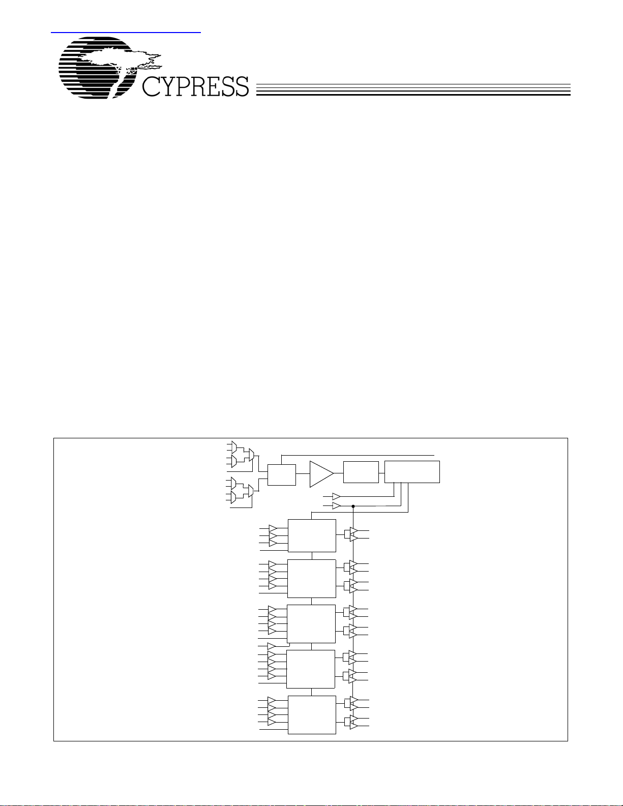
Functional
Block Diagram
Feedback Bank
FBKA+
FBKA–
FBKB+
FBKB–
FBSEL
REFA+
REFA–
REFB+
REFB–
REFSEL
Bank 4
Bank 3
Bank 2
Bank 1
FBF0
FBDS0
FBDS1
FBDIS
4F0
4F1
4DS0
4DS1
DIS4
3F0
3F1
3DS0
3DS1
DIS3
INV3
2F0
2F1
2DS0
2DS1
DIS2
1F0
1F1
1DS0
1DS1
DIS1
Phase
Freq.
Detector
OUTPUT_MODE
3
3
3
3
3
3
3
3
3
3
3
3
3
3
3
3
3
3
3
3
The CY7B993V and CY7B994V High-speed Multi-phase PLL
Clock Buffers offer user-selectable control over system clock
functions. This multiple-output clock driver provides the
system integrator with functions necessary to optimize the
timing of high-performance computer and communication
systems.
These devices feature a guaranteed maximum TTB window
specifying all occurrences of output clocks with respect to the
input reference clock across variations in output frequency,
supply voltage, operating temperature, input edge rate, and
process.
Eighteen configurable outputs each drive terminated transmission lines with impedances as low as 50Ω while delivering
minimal and specified output skews at LVTTL levels. The outputs
are arranged in five banks. Banks 1 to 4 of four outputs allow
a divide function of 1 to 12, while simultaneously allowing
phase adjustments in 625–1300-ps increments up to 10.4 ns.
One of the output banks also includes an independent clock
invert function. The feedback bank consists of two outputs,
which allows divide-by functionality from 1 to 12 and limited
phase adjustments. Any one of these eighteen outputs can be
connected to the feedback input as well as driving other inputs.
Selectable reference input is a fault tolerance feature that
allows smooth change-over to secondary clock source, when
the primary clock source is not in operation. The reference
inputs and feedback inputs are configurable to accommodate
both LVTTL or Differential (LVPECL) inputs. The completely
integrated PLL reduces jitter and simplifies board layout.
LOCK
Filter
FS
Divide and
Phase
Select
Matrix
Divide and
Phase
Select
Matrix
Divide and
Phase
Select
Matrix
Divide and
Phase
Select
Matrix
Divide and
Phase
Select
Matrix
QFA0
QFA1
4QA0
4QA1
4QB0
4QB1
3QA0
3QA1
3QB0
3QB1
2QA0
2QA1
2QB0
2QB1
1QA0
1QA1
1QB0
1QB1
Control Logic
Divide and Phase
Generator
VCO
3
3
Cypress Semiconductor Corporation • 3901 North First Street • San Jose, CA 95134 • 408-943-2600
Document #: 38-07127 Rev. *F Revised August 10, 2005
Page 2
RoboClock
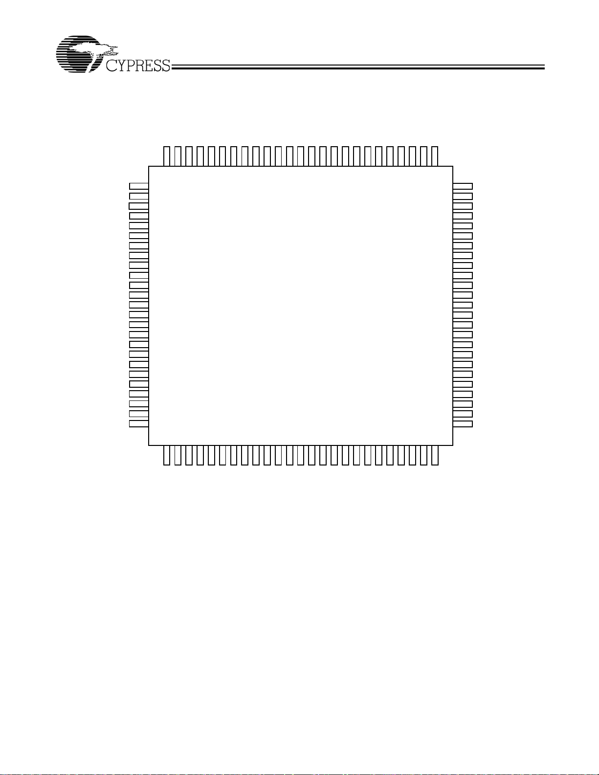
Pin Configurations
GND
3F1
4F1
3F0
4F0
4DS1
3DS1
GND
4QB1
VCCN
4QB0
GND
GND
4QA1
VCCN
4QA0
GND
2DS1
1DS1
VCCQ
4DS0
3DS0
2DS0
1DS0
GND
CY7B993V
CY7B994V
100-pin TQFP
LOCK
FBDS1
FBDS0
GND
1QB1
VCCN
GND
1QB0
1
2
3
4
5
6
7
8
9
10
11
12
13
14
15
16
17
18
19
20
21
22
23
24
25
3332313029282726
VCCN
1QA1
GND
92 91 90 848587 868889 83 82 81 7678 77798093949596979899100
GND
GND
1QA0
QFA1
QFA0
GND
VCCN
GND
FBKB+
CY7B993/4V
34 35 36 424139 403837 43 44 45 5048 494746
FBKB–
FBSEL
FBKA–
FBKA+
VCCQ
75
74
73
72
71
70
69
68
67
66
65
64
63
62
61
60
59
58
57
56
55
54
53
52
51
VCCQ
REFA+
REFA –
REFSEL
REFB–
REFB+
2F0
FS
GND
2QA0
VCCN
2QA1
GND
GND
2QB0
VCCN
2QB1
GND
FBF0
1F0
GND
VCCQ
FBDIS
DIS4
DIS3
VCCQ
VCCQ
2F1
GND
GND
GND
DIS1
DIS2
GND
3QA0
GND
GND
3QA1
VCCN
3QB0
GND
3QB1
VCCN
VCCQ
GND
INV3
OUTPUT_MODE
VCCQ
GND
1F1
Document #: 38-07127 Rev. *F Page 2 of 15
Page 3
RoboClock
Pin Configurations (continued)
12345678910
1QB1 1QB0 1QA1 1QA0 QFA0 QFA1 FBKB+ VCCQ FBKA– FBKA+
A
VCCN VCCN VCCN VCCN VCCN VCCN VCCQ FBKB– FBSEL REFA+
B
GND GND GND GND GND GND VCCQ GND GND REFA–
C
LOCK
D
4QB1 VCCN
E
4QB0 VCCN
F
4F0
(3_level)
3F1
(3_level)
4DS1
(3_level)
3DS1
(3_level)
100-lead BGA
GND
GND
GND GND GND GND
FBDS1
(3_level)
(3_level)
3F0
FBDS0
(3_level)
4F1
(3_level)
2F0
(3_level)
GND
VCCQ REFSEL REFB–
FS
(3_level)
FBF0
(3_level)
VCCN REFB+
VCCN 2QA0
CY7B993V
CY7B994V
1F0
(3_level)
FBDIS 2QB0
DIS3 2QB1
2QA1
G
H
J
K
Pin Definitions
4QA1
4QA0
4DS0
(3_level)
2F1
(3_level)
[1]
2DS1
(3_level)
1DS1
(3_level)
3DS0
(3_level)
1F1
(3_level)
VCCQ GND GND GND GND VCCQ
1DS0
(3_level)
2DS0
(3_level)
DIS2 VCCN 3QA0 3QA1 GND 3QB0 3QB1 DIS4
VCCQ GND GND VCCQ
DIS1 VCCN VCCN GND
OUTPUT
MODE
(3_level)
INV3
(3_level)
Pin Name I/O Pin Type Pin Description
FBSEL Input LVTTL Feedback Input Select: When LOW, FBKA inputs are selected. When HIGH, the FBKB
inputs are selected. This input has an internal pull-down.
FBKA+, FBKA–
FBKB+, FBKB–
Input LVTTL/
LVDI FF
Feedback Inputs: One pair of inputs selected by the FBSEL is used to feedback the clock
output xQn to the phase detector. The PLL will operate such that the rising edges of the
reference and feedback signals are aligned in both phase and frequency. These inputs
can operate as differential PECL or single-ended TTL inputs. When operating as a
single-ended LVTTL input, the complementary input must be left open.
REFA+, REFA–
REFB+, REFB–
Input LVTTL/
LVDI FF
Reference Inputs: These inputs can operate as differential PECL or single-ended TTL
reference inputs to the PLL. When operating as a single-ended LVTTL input, the complementary input must be left open.
REFSEL Input LVTTL Reference Select Input: The REFSEL input controls how the reference input is
configured. When LOW, it will use the REFA pair as the reference input. When HIGH, it
will use the REFB pair as the reference input. This input has an internal pull-down.
FS Input 3-level
Input
FBF0 Input 3-level
Input
Note:
1. For all three-state inputs, HIGH indicates a connection to V
circuitry holds an unconnected input to V
Frequency Select: This input must be set according to the nominal frequency (f
Tabl e 1).
NOM
Feedback Output Phase Function Select: This input determines the phase function of
the Feedback bank’s QFA[0:1] outputs (see Tab le 3).
, LOW indicates a connection to GND, and MID indicates an open connection. Internal termination
CC
/2.
CC
) (see
Document #: 38-07127 Rev. *F Page 3 of 15
Page 4
RoboClock
CY7B993V
CY7B994V
Input
Input
Input
Input
Input
[1]
Feedback Divider Function Select: These inputs determine the function of the QFA0
and QFA1 outputs (see Tab le 4 ).
is disabled to the “HOLD-OFF” or “HI-Z” state; the disable state is determined by
OUTPUT_MODE. When LOW, the QFA[0:1] is enabled (see Table 5). This input has an
internal pull-down.
Output Phase Function Select: Each pair controls the phase function of the respective
bank of outputs (see Tabl e 3).
Output Divider Function Select: Each pair controls the divider function of the respective
bank of outputs (see Tabl e 4).
the output bank is disabled to the “HOLD-OFF” or “HI-Z” state; the disable state is determined by OUTPUT_MODE. When LOW, the [1:4]Q[A:B][0:1] is enabled (see Table 5).
These inputs each have an internal pull-down.
Invert Mode: This input only affects Bank 3. When this input is LOW, each matched output
pair will become complementary (3QA0+, 3QA1–, 3QB0+, 3QB1–). When this input is
HIGH, all four outputs in the same bank will be inverted. When this input is MID all four
outputs will be non inverting.
reference signal. When LOW, the PLL is attempting to acquire lock.
Output Mode: This pin determines the clock outputs’ disable state. When this input is
HIGH, the clock outputs will disable to high-impedance (HI-Z). When this input is LOW,
the clock outputs will disable to “HOLD-OFF” mode. When in MID, the device will enter
factory test mode.
FB input. These outputs have numerous divide options and three choices of phase adjustments. The function is determined by the setting of the FBDS[0:1] pins and FBF0.
mined by the [1:4]DS[0:1] and [1:4]F[0:1] inputs.
Pin Definitions (continued)
Pin Name I/O Pin Type Pin Description
FBDS[0:1] Input 3-level
FBDIS Input LVTTL Feedback Disable: This input controls the state of QFA[0:1]. When HIGH, the QFA[0:1]
[1:4]F[0:1] Input 3-level
[1:4]DS[0:1] Input 3-level
DIS[1:4] Input LVTTL Output Disable: Each input controls the state of the respective output bank. When HIGH,
INV3 Input 3-level
LOCK Output LVTTL PLL Lock Indicator: When HIGH, this output indicates the internal PLL is locked to the
OUTPUT_MODE Input 3-Level
QFA[0:1] Output LVTTL Clock Feedback Output: This pair of clock outputs is intended to be connected to the
[1:4]Q[A:B][0:1] Output LVTTL Clock Output: These outputs provide numerous divide and phase select functions deter-
VCCN PWR Output Buffer Power: Power supply for each output pair.
VCCQ PWR Internal Power: Power supply for the internal circuitry.
GND PWR Device Ground.
Block Diagram Description
Phase Frequency Detector and Filter
These two blocks accept signals from the REF inputs (REFA+,
REFA–, REFB+, or REFB–) and the FB inputs (FBKA+,
FBKA–, FBKB+, or FBKB–). Correction information is then
generated to control the frequency of the voltage-controlled
oscillator (VCO). These two blocks, along with the VCO, form
a PLL that tracks the incoming REF signal.
The CY7B993V/994V have a flexible REF and FB input
scheme. These inputs allow the use of either differential
LVPECL or single-ended LVTTL inputs. To configure as
single-ended LVTTL inputs, the complementary pin must be
left open (internally pulled to 1.5V). The other input pin can
then be used as an LVTTL input. The REF inputs are also
tolerant to hot insertion.
Document #: 38-07127 Rev. *F Page 4 of 15
The REF inputs can be changed dynamically. When changing
from one reference input to the other of the same frequency,
the PLL is optimized to ensure that the clock output period will
not be less than the calculated system budget (t
(nominal reference clock period) – t
t
(max. period deviation)) while reacquiring the lock.
PDEV
VCO, Control Logic, Divider, and Phase Generator
The VCO accepts analog control inputs from the PLL filter
block. The FS control pin setting determines the nominal
operational frequency range of the divide by one output (f
of the device. f
There are two versions: a low-speed device (CY7B993V)
where f
high-speed device (CY7B994V) that ranges from 24 MHz to
200 MHz. The FS setting for each device is shown in Ta bl e 1.
The f
the CY7B994V, the upper f
200 MHz.
NOM
frequency is seen on “divide-by-one” outputs. For
NOM
is directly related to the VCO frequency.
NOM
ranges from 12 MHz to 100 MHz, and a
range extends from 96 MHz to
NOM
(cycle-to-cycle jitter) –
CCJ
MIN
= t
REF
NOM
)
Page 5
RoboClock
Table 1. Frequency Range Select
CY7B993V CY7B994V
f
(MHz) f
NOM
Min. Max. Min. Max.
FS
[2]
LOW12262452
MID 24 52 48 100
HIGH 48 100 96 200
Time Unit Definition
Selectable skew is in discrete increments of time unit (t
value of a t
nominal output frequency. The equation to be used to
determine the t
t
= 1/(f
U
is determined by the FS setting and the maximum
U
value is as follows:
U
*N).
NOM
N is a multiplication factor which is determined by the FS
setting. f
in Table 2 .
is nominal frequency of the device. N is defined
NOM
Table 2. N Factor Determination
CY7B993V CY7B994V
f
(MHz) at
FS
N
NOM
which tU =1.0 ns N
LOW 64 15.625 32 31.25
MID 32 31.25 16 62.5
HIGH 16 62.5 8 125
Divide and Phase Select Matrix
The Divide and Phase Select Matrix is comprised of five
independent banks: four banks of clock outputs and one bank
for feedback. Each clock output bank has two pairs of
low-skew, high-fanout output buffers ([1:4]Q[A:B][0:1]), two
phase function select inputs ([1:4]F[0:1]), two divider function
selects ([1:4]DS[0:1]), and one output disable (DIS[1:4]).
The feedback bank has one pair of low-skew, high-fanout
output buffers (QFA[0:1]). One of these outputs may connect
to the selected feedback input (FBK[A:B]±). This feedback
bank also has one phase function select input (FBF0), two
divider function selects FSDS[0:1], and one output disable
(FBDIS).
The phase capabilities that are chosen by the phase function
select pins are shown in Tabl e 3. The divide capabilities for
each bank are shown in Table 4.
Notes:
2. The level to be set on FS is determined by the “nominal” operating frequency (f
the output is operating in the undivided mode. The REF and FB are at f
3. BK1, BK2 denotes following the skew setting of Bank1 and Bank2, respectively.
(MHz)
NOM
). The
U
f
(MHz) at
NOM
which tU =1.0 ns
NOM
when the output connected to FB is undivided.
CY7B993V
CY7B994V
Table 3. Output Skew Select Function
Function
Selects Output Skew Function
[1:4]F0
[1:4]F1
LOW LOW –4t
LOW MID –3t
LOW HIGH –2t
MID LOW –1t
MID MID 0t
MID HIGH +1t
HIGH LOW +2t
HIGH MID +3t
HIGH HIGH +4t
and
FBF0 Bank1 Bank2 Bank3 Bank4
U
U
U
U
U
U
U
U
U
–4t
–3tu –7t
–2t
–1tUBK1
0t
+1tUBK2
+2t
+3t
+4t
–8t
U
–6t
U
0t
U
+6t
U
+7t
U
+8t
U
–8t
U
–7t
U
–6t
U
[3]
BK1
0t
U
[3]
BK2
+6t
U
+7t
U
+8t
U
Table 4. Output Divider Function
Function
Selects Output Divider Function
[1:4]DS1
and
FBDS1
[1:4]DS0
and
FBDS0
Bank1Bank2Bank3Bank
LOW LOW /1 /1 /1 /1 /1
LOW MID /2 /2 /2 /2 /2
LOW HIGH /3 /3 /3 /3 /3
MID LOW /4 /4 /4 /4 /4
MID MID /5 /5 /5 /5 /5
MID HIGH /6 /6 /6 /6 /6
HIGHLOW/8/8/8/8 /8
HIGH MID /10 /10 /10 /10 /10
HIGH HIGH /12 /12 /12 /12 /12
Figure 1 illustrates the timing relationship of programmable
skew outputs. All times are measured with respect to REF with
the output used for feedback programmed with 0t
PLL naturally aligns the rising edge of the FB input and REF
input. If the output used for feedback is programmed to
another skew position, then the whole t
respect to REF. For example, if the output used for feedback
matrix will shift with
U
is programmed to shift –8tU, then the whole matrix is shifted
forward in time by 8t
of skew will effectively be skewed 16tU with respect to REF.
) of the VCO and Phase Generator. f
NOM
. Thus an output programmed with 8t
U
always appears on an output when
NOM
Feed-
back
Bank
–4t
U
U
U
[3]
U
[3]
U
U
+4t
U
Feed-
back
4
Bank
skew. The
U
NA
NA
NA
0tu
NA
NA
NA
U
U
U
Document #: 38-07127 Rev. *F Page 5 of 15
Page 6
RoboClock
1F[1:0]
2F[1:0]
(N/A)
(N/A)
(N/A)
LL
LM
LH
ML
MM
MH
HL
HM
HH
(N/A)
(N/A)
(N/A)
3F[1:0]
4F[1:0]
LL
LM
LH
(N/A)
(N/A)
(N/A)
(N/A)
MM
(N/A)
(N/A)
(N/A)
(N/A)
HL
HM
HH
FBInput
REFInput
–8t
–7t
–6t
–4t
–3t
–2t
–1t
0t
+1t
+2t
+3t
+4t
+6t
+7t
+8t
CY7B993V
CY7B994V
U
+7t
t
U
+8t
0
0
t
U
U
U
U
U
– 2t
0
t
U
– 1t
0
t
t 0t
U
+1t
+2tU+3tU+4tU+5tU+6t
0
t 0t 0t 0t 0t
U
0
U
U
– 6t
– 5t
– 4t
– 8t
– 7t
0
0
0
t
t
U
U
U
U
U
U
U
U
U
U
U
U
U
U
U
0
t
t
– 3t
0
0
t
t
Figure 1. Typical Outputs with FB Connected to a Zero-Skew Output
Output Disable Description
The feedback Divide and Phase Select Matrix Bank has two
outputs, and each of the four Divide and Phase Select Matrix
Banks have four outputs. The outputs of each bank can be
independently put into a HOLD-OFF or high-impedance state.
The combination of the OUTPUT_MODE and DIS[1:4]/FBDIS
inputs determines the clock outputs’ state for each bank. When
the DIS[1:4]/FBDIS is LOW, the outputs of the corresponding
bank will be enabled. When the DIS[1:4]/FBDIS is HIGH, the
outputs for that bank will be disabled to a high-impedance
(HI-Z) or HOLD-OFF state depending on the OUTPUT_MODE
input. Tabl e 5 defines the disabled output functions.
The HOLD-OFF state is intended to be a power saving feature.
An output bank is disabled to the HOLD-OFF state in a
HOLD-OFF state, non-inverting outputs are driven to a logic
LOW state on its falling edge. Inverting outputs are driven to a
logic HIGH state on its rising edge. This ensures the output
clocks are stopped without glitch. When a bank of outputs is
disabled to HI-Z state, the respective bank of outputs will go
HI-Z immediately.
Table 5. DIS[1:4]/FBDIS Pin Functionality
OUTPUT_MODE DIS[1:4]/FBDIS Output Mode
HIGH/LOW LOW ENABLED
HIGH HIGH HI-Z
LOW HIGH HOLD-OFF
MID X FACTORY TEST
[4]
maximum of six output clock cycles from the time when the
disable input (DIS[1:4]/FBDIS) is HIGH. When disabled to the
Note:
4. FB connected to an output selected for “Zero” skew (i.e., FBF0 = MID or XF[1:0] = MID).
Document #: 38-07127 Rev. *F Page 6 of 15
Page 7

RoboClock
INV3 Pin Function
Bank3 has signal invert capability. The four outputs of Bank3
will act as two pairs of complementary outputs when the INV3
pin is driven LOW. In complementary output mode, 3QA0 and
3QB0 are non-inverting; 3QA1and 3QB1 are inverting outputs.
All four outputs will be inverted when the INV3 pin is driven
HIGH. When the INV3 pin is left in MID, the outputs will not
invert. Inversion of the outputs are independent of the skew
and divide functions. Therefore, clock outputs of Bank3 can be
inverted, divided, and skewed at the same time.
Lock Detect Output Description
The LOCK detect output indicates the lock condition of the
integrated PLL. Lock detection is accomplished by comparing
the phase difference between the reference and feedback
inputs. Phase error is declared when the phase difference
between the two inputs is greater than the specified device
propagation delay limit (t
PD
).
When in the locked state, after four or more consecutive
feedback clock cycles with phase-errors, the LOCK output will
be forced LOW to indicate out-of-lock state.
When in the out-of-lock state, 32 consecutive phase-errorless
feedback clock cycles are required to allow the LOCK output
to indicate lock condition (LOCK = HIGH).
If the feedback clock is removed after LOCK has gone HIGH,
a “Watchdog” circuit is implemented to indicate the out-of-lock
condition after a time-out period by deasserting LOCK LOW.
This time out period is based upon a divided down reference
clock.
This assumes that there is activity on the selected REF input.
If there is no activity on the selected REF input then the LOCK
detect pin may not accurately reflect the state of the internal
PLL.
Factory Test Mode Description
The device will enter factory test mode when the
OUTPUT_MODE is driven to MID. In factory test mode, the
device will operate with its internal PLL disconnected; input
level supplied to the reference input will be used in place of the
PLL output. In TEST mode the selected FB input(s) must be
tied LOW. All functions of the device are still operational in
factory test mode except the internal PLL and output bank
disables. The OUTPUT_MODE input is designed to be a static
input. Dynamically toggling this input from LOW to HIGH may
temporarily cause the device to go into factory test mode
(when passing through the MID state).
CY7B993V
CY7B994V
Factory Test Reset
When in factory test mode (OUTPUT_MODE = MID), the
device can be reset to a deterministic state by driving the DIS4
input HIGH. When the DIS4 input is driven HIGH in factory test
mode, all clock outputs will go to HI-Z; after the selected
reference clock pin has five positive transitions, all the internal
finite state machines (FSM) will be set to a deterministic state.
The deterministic state of the state machines will depend on
the configurations of the divide selects, skew selects, and
frequency select input. All clock outputs will stay in
high-impedance mode and all FSMs will stay in the deterministic state until DIS4 is deasserted. When DIS4 is deasserted
(with OUTPUT_MODE still at MID), the device will re-enter
factory test mode.
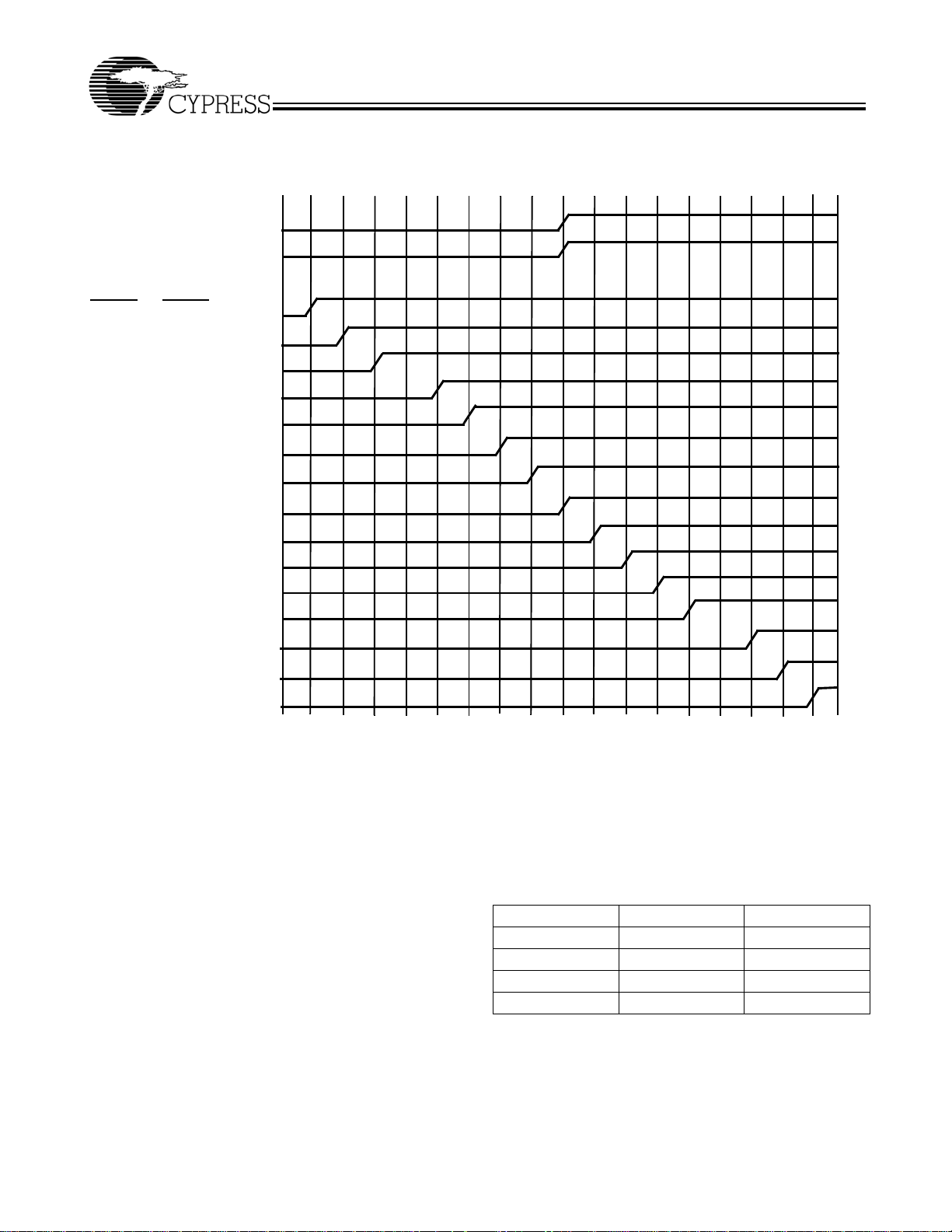
Safe Operating Zone
Figure 2 illustrates the operating condition at which the device
does not exceed its allowable maximum junction temperature
of 150°C. Figure 2 shows the maximum number of outputs that
can operate at 185 MHz (with 25-pF load and no air flow) or
200 MHz (with 10-pF load and no air flow) at various ambient
temperatures. At the limit line, all other outputs are configured
to divide-by-two (i.e., operating at 92.5 MHz) or lower
frequencies. The device will operate below maximum
allowable junction temperature of 150°C when its configuration (with the specified constraints) falls within the shaded
region (safe operating zone). Figure 2 shows that at 85°C, the
maximum number of outputs that can operate at 200 MHz is
6; and at 70°C, the maximum number of outputs that can
operate at 185 MHz is 16 (with 25-pF load and 0-m/s air flow).
Typical Safe Operating Zone
(25-pF Load, 0-m /s air flow )
100
95
90
85
80
75
70
65
60
55
Ambient Temperature (C)
50
Safe Operating Zone
24681012141618
Numb e r of Outputs at 185 M Hz
Figure 2. Typical Safe Operating Zone
Document #: 38-07127 Rev. *F Page 7 of 15
Page 8
RoboClock
CY7B993V
CY7B994V
Absolute Maximum Conditions
[5]
(Above which the useful life may be impaired. For user guidelines, not tested.)
Storage Temperature ................................–40°C to + 125°C
Ambient Temperature with
Power Applied............................................ –40°C to + 125°C
Supply Voltage to Ground Potential.............. –0.5V to + 4.6V
DC Input Voltage ....................................–0.3V to V
CC
+ 0.5V
Electrical Characteristics Over the Operating Range
Parameter Description Test Conditions Min. Max. Unit
LVTTL Compatible Output Pins (QFA[0:1], [1:4]Q[A:B][0:1], LOCK)
V
OH
V
OL
I
OZ
LVTTL Compatible Input Pins (FBKA±, FBKB±, REFA±, REFB±, FBSEL, REFSEL, FBDIS, DIS[1:4])
V
IH
V
IL
I
I
I
lH
I
lL
Three-level Input Pins (FBF0, FBDS[0:1], [1:4]F[0:1], [1:4]DS[0:1], FS, OUTPUT_MODE(TEST))
V
IHH
V
IMM
V
ILL
I
IHH
I
IMM
I
ILL
LVDIFF Input Pins (FBK[A:B]±, REF[A:B]±)
V
DIFF
V
IHHP
V
ILLP
V
COM
Notes:
5. Multiple Supplies: The voltage on any input or I/O pin cannot exceed the power pin during power-up. Power supply sequencing is NOT required.
6. These inputs are normally wired to V
the unconnected inputs at V
before all data sheet limits are achieved.
LVTTL HIGH Voltage QFA[0:1], [1:4]Q[A:B][0:1] VCC = Min., I
LOCK I
LVTTL LOW Voltage QFA[0:1], [1:4]Q[A:B][0:1] VCC = Min., IOL= 30 mA – 0.5 V
LOCK I
High-impedance State Leakage Current –100 100 µA
LVTTL Input HIGH FBK[A:B]±, REF[A:B]± Min. < VCC < Max. 2.0 V
REFSEL, FBSEL, FBDIS,
DIS[1:4]
LVTTL Input LOW FBK[A:B]±, REF[A:B]± Min. < VCC < Max. –0.3 0.8 V
REFSEL, FBSEL, FBDIS, DIS[1:4] –0.3 0.8 V
LVTTL VIN >V
CC
LVTTL Input HIGH
Current
LVTTL Input LOW
Current
Three-level Input HIGH
Three-level Input MID
Three-level Input LOW
Three-level Input
HIGH Current
Three-level Input
MID Current
Three-level Input
LOW Current
FBK[A:B]±, REF[A:B]± VCC = GND, VIN = 3.63V – 100 µA
FBK[A:B]±, REF[A:B]± VCC = Max., VIN = V
REFSEL, FBSEL, FBDIS, DIS[1:4] V
FBK[A:B]±, REF[A:B]± VCC = Max., VIN = GND –500 – µA
REFSEL, FBSEL, FBDIS, DIS[1:4] –500 – µA
[6]
[6]
[6]
Three-level input pins excl. FBF0 VIN = V
FBF0 – 400 µA
Three-level input pins excl. FBF0 VIN = VCC/2 –50 50 µA
FBF0 –100 100 µA
Three-level input pins excl. FBF0 VIN = GND –200 – µA
FBF0 –400 – µA
Input Differential Voltage 400 V
Highest Input HIGH Voltage 1.0 V
Lowest Input LOW Voltage GND V
Common Mode Range (crossing voltage) 0.8 V
, GND, or left unconnected (actual threshold voltages vary as a percentage of VCC). Internal termination resistors hold
CC
/2. If these inputs are switched, the function and timing of the outputs may glitch and the PLL may require an additional t
CC
Output Current into Outputs (LOW)............................. 40 mA
Static Discharge Voltage........................................... > 1100V
(per MIL-STD-883, Method 3015)
Latch-up Current.................................................. > ± 200 mA
Operating Range
Range Ambient Temperature V
Commercial 0°C to +70°C 3.3V ± 10%
Industrial –40°C to +85°C 3.3V ± 10%
= –30 mA 2.4
OH
= –2 mA, VCC = Min. 2.4 – V
OH
= 2 mA, VCC = Min. – 0.5 V
OL
2.0 V
CC
= V
IN
CC
Min. < VCC < Max. 0.87*V
– 500 µA
– 500 µA
CC
Min. < VCC < Max. 0.47*VCC0.53*V
Min. < VCC < Max. – 0.13*V
CC
– 200 µA
CC
–V
+ 0.3 V
CC
+ 0.3 V
CC
–V
CC
CC
CC
CC
– 0.4 V
CC
CC
LOCK
V
V
mV
V
V
time
Document #: 38-07127 Rev. *F Page 8 of 15
Page 9
RoboClock
CY7B993V
CY7B994V
Electrical Characteristics Over the Operating Range (continued)
Parameter Description Test Conditions Min. Max. Unit
Operating Current
I
CCI
I
CCN
Capacitance
Internal Operating
Current
Output Current
Dissipation/Pair
[8]
CY7B993V V
= Max., f
CC
CY7B994V – 250 mA
CY7B993V V
CY7B994V – 50 mA
= Max.,
CC
C
= 25 pF,
LOAD
= 50Ω at VCC/2,
R
LOAD
f
MAX
Parameter Description Test Conditions Min. Max. Unit
C
IN
Switching Characteristics Over the Operating Range
Input Capacitance TA = 25°C, f = 1 MHz, VCC = 3.3V 5 pF
[9, 10, 11, 12, 13]
CY7B993/4V-2 CY7B993/4V-5
Parameter Description
f
in
Clock Input Frequency CY7B993V 12 – 100 12 – 100 MHz
CY7B994V 24 – 200 24 – 200 MHz
f
out
Clock Output Frequency CY7B993V 12 – 100 12 – 100 MHz
CY7B994V 24 – 200 24 – 200 MHz
[14, 15]
[14, 15]
)
CC
[14, 15]
[14, 15]
/2.
[14, 15]
[14, 15]
[14, 15, 16, 17]
– – 200 – – 200 ps
– – 200 – – 250 ps
– – 250 – – 550 ps
– – 250 – – 650 ps
– – 250 – – 700 ps
– – 500 – – 800 ps
– – 200 – – 300 ps
– 50 150 – 50 150 ps Peak
– 50 100 – 50 100 ps Peak
NOM
t
SKEWPR
t
SKEWBNK
t
SKEW0
t
SKEW1
t
SKEW2
Matched-Pair Skew
Intrabank Skew
Output-Output Skew (same frequency and phase, rise to
rise, fall to fall)
Output-Output Skew (same frequency and phase, other
banks at different frequency, rise to rise, fall to fall)
Output-Output Skew (invert to nominal of different banks,
compared banks at same frequency, rising edge to falling
edge aligned, other banks at same frequency)
t
SKEW3
t
SKEWCPR
t
CCJ1-3
t
CCJ4-12
t
PD
Notes:
7. I
CCI
CY7B994V), and all other clock output banks to run at half the maximum frequency. FS and OUTPUT_MODE are asserted to the HIGH state.
8. This is dependent upon frequency and number of outputs of a bank being loaded. The value indicates maximum I
load of 25 pF terminated to 50Ω at V
9. This is for non-three level inputs.
10. Assumes 25-pF max. load capacitance up to 185 MHz. At 200 MHz the max. load is 10 pF.
11. Both outputs of pair must be terminated, even if only one is being used.
12. Each package must be properly decoupled.
13. AC parameters are measured at 1.5V unless otherwise indicated.
14. Test Load C
15. SKEW is defined as the time between the earliest and the latest output transition among all outputs for which the same phase delay has been selected when
all outputs are loaded with 25 pF and properly terminated up to 185 MHz. At 200 MHz the max load is 10 pF.
16. Complementary output skews are measured at complementary signal pair intersections.
17. Guaranteed by statistical correlation. Tested initially and after any design or process changes that may affect these parameters.
Output-Output Skew (all output configurations outside of
t
and t
SKEW1
SKEW2
Complementary Outputs Skew (crossing to crossing,
complementary outputs of the same bank)
Cycle-to-Cycle Jitter (divide by 1 output frequency,
FB = divide by 1, 2, 3)
Cycle-to-Cycle Jitter (divide by 1 output frequency,
FB = divide by 4, 5, 6, 8, 10, 12)
Propagation Delay, REF to FB Rise –250 – 250 –500 – 500 ps
measurement is performed with Bank1 and FB Bank configured to run at maximum frequency (f
= 25 pF, terminated to VCC/2 with 50Ω up to185 MHz and 10-pF load to 200 MHz.
L
MAX
[7]
– 250 mA
–40mA
= 100 MHz for CY7B993V, f
at maximum frequency and maximum
CCN
= 200 MHz for
NOM
UnitMin. Typ. Max. Min. Typ. Max.
Document #: 38-07127 Rev. *F Page 9 of 15
Page 10
RoboClock
Switching Characteristics Over the Operating Range
Parameter Description
TTB Total Timing Budget window (same frequency and phase)
t
PDDELTA
t
REFpwh
t
REFpwl
t
r/tf
t
LOCK
t
RELOCK1
t
RELOCK2
t
ODCV
t
PWH
t
PWL
t
PDEV
t
OAZ
t
OAZ
18]
Propagation Delay difference between two devices
REF input (Pulse Width HIGH)
REF input (Pulse Width LOW)
Output Rise/Fall Time
[20]
[19]
[19]
PLL Lock Time From Power-up – – 10 – – 10 ms
PLL Relock Time (from same frequency, different phase)
with Stable Power Supply
PLL Relock Time (from different frequency, different phase)
with Stable Power Supply
Output duty cycle deviation from 50%
Output HIGH time deviation from 50%
Output LOW time deviation from 50%
Period deviation when changing from reference to
reference
DIS[1:4]/FBDIS HIGH to output high-impedance from
ACTIVE
DIS[1:4]/FBDIS LOW to output ACTIVE from output
high-impedance
[23]
[14, 24]
[24, 25]
[21]
[13]
[22]
[22]
[9, 10, 11, 12, 13]
[17]
CY7B993V
CY7B994V
(continued)
CY7B993/4V-2 CY7B993/4V-5
UnitMin. Typ. Max. Min. Typ. Max.
[17,
– – 500 – – 700 ps
– – 200 – – 200 ps
2.0 – – 2.0 – – ns
2.0 – – 2.0 – – ns
0.15 – 2.0 0.15 – 2.0 ns
– 500 – 500 µs
– 1000 – 1000 µs
–1.0 1.0 –1.0 1.0 ns
–1.5– 1.5ns
–2.0– 2.0ns
– 0.025 – 0.025 UI
1.0 10 1.0 10 ns
0.5 14 0.5 14 ns
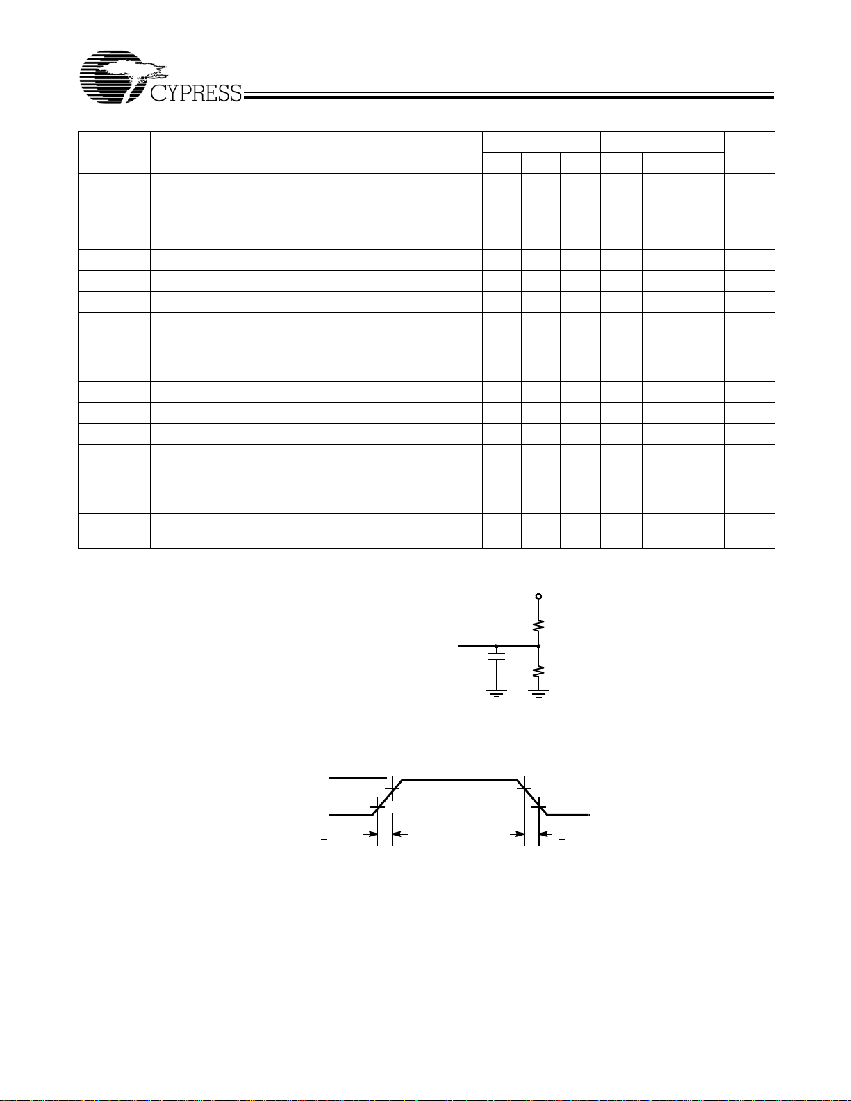
AC Test Loads and Waveform
For LOCK output only For all other outputs
R1 = 910Ω
R2 = 910Ω
<30pF
C
L
(Includes fixture and
probe capacitance)
[26]
R1 = 100Ω
R2 = 100Ω
CL< 25 pF to 185 MHz
or 10 pF at 200 MHz
(a) LVTTL
3.3V
GND
< 1ns < 1 ns
OUTPUT
AC Test Load
2.0V
0.8V
3.3V
R1
C
L
R2
2.0V
0.8V
(b) TTL Input Test Waveform
Notes:
18. TTB is the window between the earliest and the latest output clocks with respect to the input reference clock across variations in output frequency, supply voltage,
operating temperature, input clock edge rate, and process. The measurements are taken with the AC test load specified and include output-output skew, cycle-cycle
jitter, and dynamic phase error. TTB will be equal to or smaller than the maximum specified value at a given frequency.
19. Tested initially and after any design or process changes that may affect these parameters.
20. Rise and fall times are measured between 2.0V and 0.8V.
must be within the frequency range defined by the same FS state.
21. f
NOM
is measured at 2.0V. t
22. t
PWH
23. UI = Unit Interval. Examples: 1 UI is a full period. 0.1UI is 10% of period.
24. Measured at 0.5V deviation from starting voltage.
25. For t
26. These figures are for illustrations only. The actual ATE loads may vary.
minimum, CL = 0 pF. For t
OZA
is measured at 0.8V.
PWL
maximum, CL= 25 pF to 185 MHz or 10 pF to 200 MHz.
OZA
Document #: 38-07127 Rev. *F Page 10 of 15
Page 11

RoboClock
AC Timing Diagrams
t
REFpwh
REF
t
PD
2.0V
FB
Q
REF TO DEVICE 1 and 2
t
PD
FB DEVICE1
t
PDELTA
FB DEVICE2
t
PWH
[13]
t
REFpwl
t
PDELTA
t
PWL
0.8V
t
CCJ1-3,4-12
CY7B993V
CY7B994V
QFA0 or
[1:4]Q[A:B]0
t
SKEWPR
QFA1 or
[1:4]Q[A:B]1
[1:4]QA[0:1]
t
SKEWBNK
[1:4]QB[0:1]
Q
t
SKEW0,1
Other Q
t
ODCV
t
SKEWPR
t
SKEWBNK
t
ODCV
t
SKEW0,1
t
SKEW2
INVERTED Q
Q
t
SKEW2
COMPLEMENTARY A
COMPLEMENTARY B
crossing
Ordering Information
Propagation
Delay (ps)
250 100 CY7B993V-2AC 100-lead Thin Quad Flat Pack Commercial
250 100 CY7B993V-2ACT 100-lead Thin Quad Flat Pack - Tape and Reel Commercial
250 100 CY7B993V-2AI 100-lead Thin Quad Flat Pack Industrial
250 100 CY7B993V-2AIT 100-lead Thin Quad Flat Pack - Tape and Reel Industrial
250 200 CY7B994V-2AC 100-lead Thin Quad Flat Pack Commercial
250 200 CY7B994V-2ACT 100-lead Thin Quad Flat Pack - Tape and Reel Commercial
250 200 CY7B994V-2BBC 100-ball Thin Ball Grid Array Commercial
250 200 CY7B994V-2BBCT 100-ball Thin Ball Grid Array - Tape and Reel Commercial
250 200 CY7B994V-2AI 100-lead Thin Quad Flat Pack Industrial
250 200 CY7B994V-2AIT 100-lead Thin Quad Flat Pack - Tape and Reel Industrial
250 200 CY7B994V-2BBI 100-ball Thin Ball Grid Array Industrial
250 200 CY7B994V-2BBIT 100-ball Thin Ball Grid Array -Tape and Reel Industrial
Max. Speed
(MHz) Ordering Code Package Type Operating Range
t
SKEWCPR
crossing
Document #: 38-07127 Rev. *F Page 11 of 15
Page 12
RoboClock
Ordering Information (continued)
Propagation
Delay (ps)
500 100 CY7B993V-5AC 100-lead Thin Quad Flat Pack Commercial
500 100 CY7B993V-5ACT 100-lead Thin Quad Flat Pack - Tape and Reel Commercial
500 100 CY7B993V-5AI 100-lead Thin Quad Flat Pack Industrial
500 100 CY7B993V-5AIT 100-lead Thin Quad Flat Pack - Tape and Reel Industrial
500 200 CY7B994V-5AC 100-lead Thin Quad Flat Pack Commercial
500 200 CY7B994V-5ACT 100-lead Thin Quad Flat Pack - Tape and Reel Commercial
500 200 CY7B994V-5BBC 100-ball Thin Ball Grid Array Commercial
500 200 CY7B994V-5BBCT 100-ball Thin Ball Grid Array - Tape and Reel Commercial
500 200 CY7B994V-5BBI 100-ball Thin Ball Grid Array Industrial
500 200 CY7B994V-5BBIT 100-ball Thin Ball Grid Array -Tape and Reel Industrial
500 200 CY7B994V-5AI 100-lead Thin Quad Flat Pack Industrial
500 200 CY7B994V-5AIT 100-lead Thin Quad Flat Pack - Tape and Reel Industrial
Lead-free
250 100 CY7B993V-2AXC 100-lead Thin Quad Flat Pack Commercial
250 100 CY7B993V-2AXCT 100-lead Thin Quad Flat Pack - Tape and Reel Commercial
250 100 CY7B993V-2AXI 100-lead Thin Quad Flat Pack Industrial
250 100 CY7B993V-2AXIT 100-lead Thin Quad Flat Pack - Tape and Reel Industrial
250 200 CY7B994V-2AXC 100-lead Thin Quad Flat Pack Commercial
250 200 CY7B994V-2AXCT 100-lead Thin Quad Flat Pack - Tape and Reel Commercial
250 200 CY7B994V-2BBXC 100-ball Thin Ball Grid Array Commercial
250 200 CY7B994V-2BBXCT 100-ball Thin Ball Grid Array - Tape and Reel Commercial
250 200 CY7B994V-2AXI 100-lead Thin Quad Flat Pack Industrial
250 200 CY7B994V-2AXIT 100-lead Thin Quad Flat Pack - Tape and Reel Industrial
250 200 CY7B994V-2BBXI 100-ball Thin Ball Grid Array Industrial
250 200 CY7B994V-2BBXIT 100-ball Thin Ball Grid Array -Tape and Reel Industrial
500 100 CY7B993V-5AXC 100-lead Thin Quad Flat Pack Commercial
500 100 CY7B993V-5AXCT 100-lead Thin Quad Flat Pack - Tape and Reel Commercial
500 100 CY7B993V-5AXI 100-lead Thin Quad Flat Pack Industrial
500 100 CY7B993V-5AXIT 100-lead Thin Quad Flat Pack - Tape and Reel Industrial
500 200 CY7B994V-5AXC 100-lead Thin Quad Flat Pack Commercial
500 200 CY7B994V-5AXCT 100-lead Thin Quad Flat Pack - Tape and Reel Commercial
500 200 CY7B994V-5BBXC 100-ball Thin Ball Grid Array Commercial
500 200 CY7B994V-5BBXCT 100-ball Thin Ball Grid Array -Tape and Reel Commercial
500 200 CY7B994V-5BBXI 100-ball Thin Ball Grid Array Industrial
500 200 CY7B994V-5BBXIT 100-ball Thin Ball Grid Array - Tape and Reel Industrial
500 200 CY7B994V-5AXI 100-lead Thin Quad Flat Pack Industrial
500 200 CY7B994V-5AXIT 100-lead Thin Quad Flat Pack - Tape and Reel Industrial
Max. Speed
(MHz) Ordering Code Package Type Operating Range
CY7B993V
CY7B994V
Document #: 38-07127 Rev. *F Page 12 of 15
Page 13

RoboClock
Package Diagrams
100-pin Thin Plastic Quad Flat Pack (TQFP) A100
CY7B993V
CY7B994V
51-85048-*B
Document #: 38-07127 Rev. *F Page 13 of 15
Page 14

RoboClock
Package Diagrams (continued)
100-ball Thin Ball Grid Array (11 x 11 x 1.4 mm) BB100
CY7B993V
CY7B994V
51-85107-*B
RoboClock is a registered trademark, and TTB and Total Timing Budget are trademarks, of Cypress Semiconductor. All product
and company names mentioned in this document are the trademarks of their respective holders.
Document #: 38-07127 Rev. *F Page 14 of 15
© Cypress Semiconductor Corporation, 2005. The information contained herein is subject to change without notice. Cypress Semiconductor Corporation assumes no responsibility for the use
of any circuitry other than circuitry embodied in a Cypress product. Nor does it convey or imply any license under patent or other rights. Cypress products are not warranted nor intended to be
used for medical, life support, life saving, critical control or safety applications, unless pursuant to an express written agreement with Cypress. Furthermore, Cypress does not authorize its
products for use as critical components in life-support systems where a malfunction or failure may reasonably be expected to result in significant injury to the user. The inclusion of Cypress
products in life-support systems application implies that the manufacturer assumes all risk of such use and in doing so indemnifies Cypress against all charges.
Page 15

RoboClock
Document History Page
Document Title: RoboClock CY7B994V/CY7B993V High-speed Multi-phase PLL Clock Buffer
Document Number: 38-07127
REV. ECN NO. Issue Date
** 109957 12/16/01 SZV Changed from Spec number: 38-00747 to 38-07127
*A 114376 05/06/02 CTK Added three industrial packages
*B 116570 09/04/02 HWT Added TTB Features
*C 122794 12/14/02 RBI Power-up requirements to operating conditions information
*D 123694 03/04/03 RGL Added min. F
*E 128462 07/29/03 RGL Added clock input frequency (f
*F 391560 See ECN RGL Added Lead-free devices
Orig. of
Change Description of Change
value of 12 MHz for CY7B993V and 24 MHz for CY7B994V
to switching characteristics table
Corrected prop delay limit parameter from (t
Output Description paragraph
table
Added typical values for jitter
out
,M,H) to t
PDSL
) specifications in the switching characteristics
in
CY7B993V
CY7B994V
in the Lock Detect
PD
Document #: 38-07127 Rev. *F Page 15 of 15
 Loading...