

Page 1
CY7B9910
CY7B9920
Low Skew Clock Buffer
Features
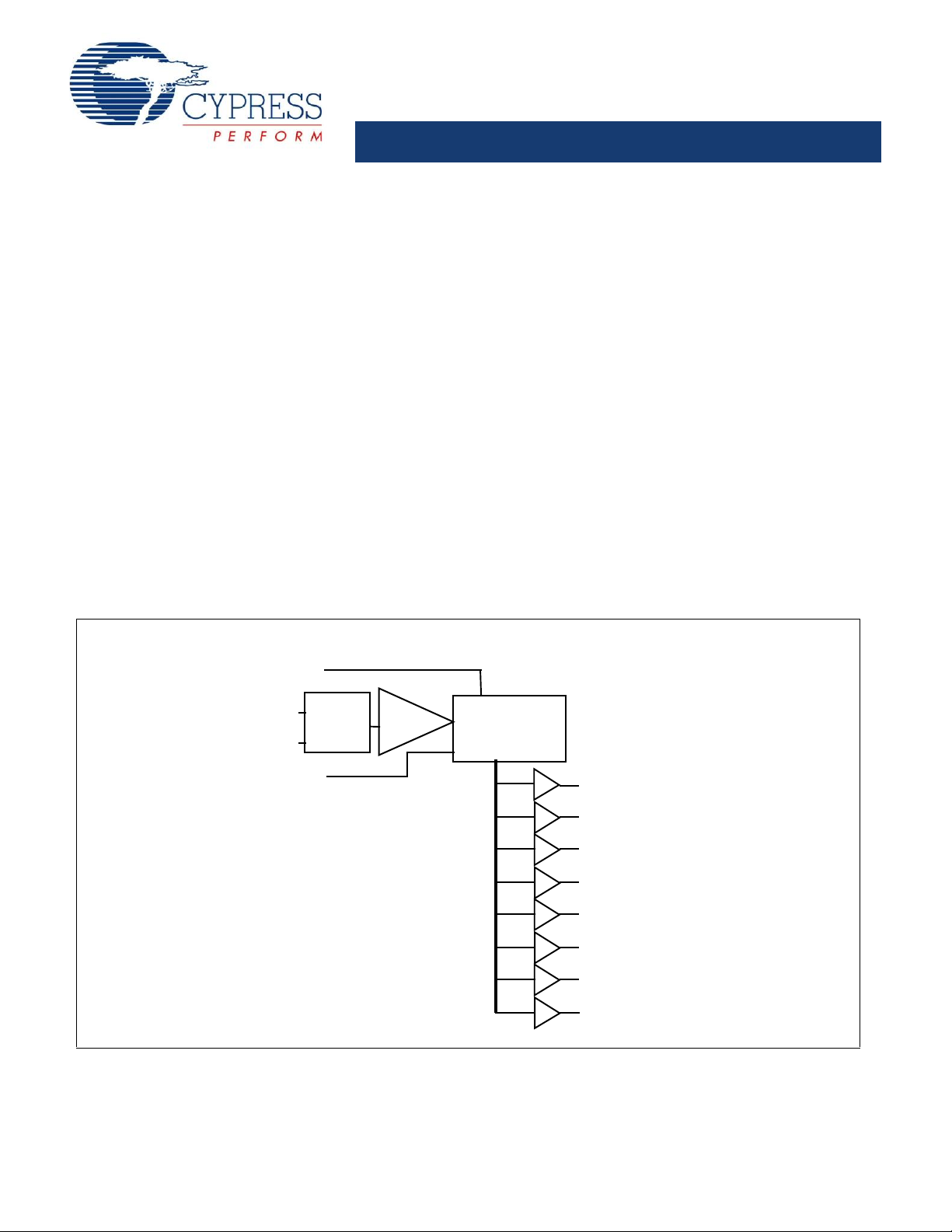
TEST
FB
REF
VOLTAGE
CONTROLLED
OSCILLATOR
FS
Q0
FILTER
PHASE
FREQ
DET
Q1
Q2
Q3
Q4
Q5
Q6
Q7
Logic Block Diagram
■ All outputs skew <100 ps typical (250 max.)
■ 15 to 80 MHz output operation
■ Zero input to output delay
■ 50% duty cycle outputs
■ Outputs drive 50Ω terminated lines
■ Low operating current
■ 24-pin SOIC package
■ Jitter:<200 ps peak to peak, <25 ps RMS
Functional Description
The completely integrated PLL enables “zero delay” capability.
External divide capability, combined with the internal PLL, allows
distribution of a low frequency clock that is multiplied by virtually
any factor at the clock destination. This facility minimizes clock
distribution difficulty while allowing maximum system clock
speed and flexibility.
Block Diagram Description
Phase Frequency Detector and Filter
The Phase Frequency Detector and Filter blocks accept inputs
from the reference frequency (REF) input and the feedback (FB)
input and generate correction information to control the
frequency of the Voltage Controlled Oscillator (VCO). These
blocks, along with the VCO, form a Phase Locked Loop (PLL)
that tracks the incoming REF signal.
The CY7B9910 and CY7B9920 Low Skew Clock Buffers offer
low skew system clock distribution. These multiple output clock
drivers optimize the timing of high performance computer
systems. Each of the eight individual drivers can drive terminated
transmission lines with impedances as low as 50Ω. They deliver
minimal and specified output skews and full swing logic levels
(CY7B9910 TTL or CY7B9920 CMOS).
VCO
The VCO accepts analog control inputs from the PLL filter block
and generates a frequency. The operational range of the VCO is
determined by the FS control pin.
Cypress Semiconductor Corporation • 198 Champion Court • San Jose, CA 95134-1709 • 408-943-2600
Document Number: 38-07135 Rev. *B Revised August 07, 2007
[+] Feedback [+] Feedback
Page 2
CY7B9910
CY7B9920
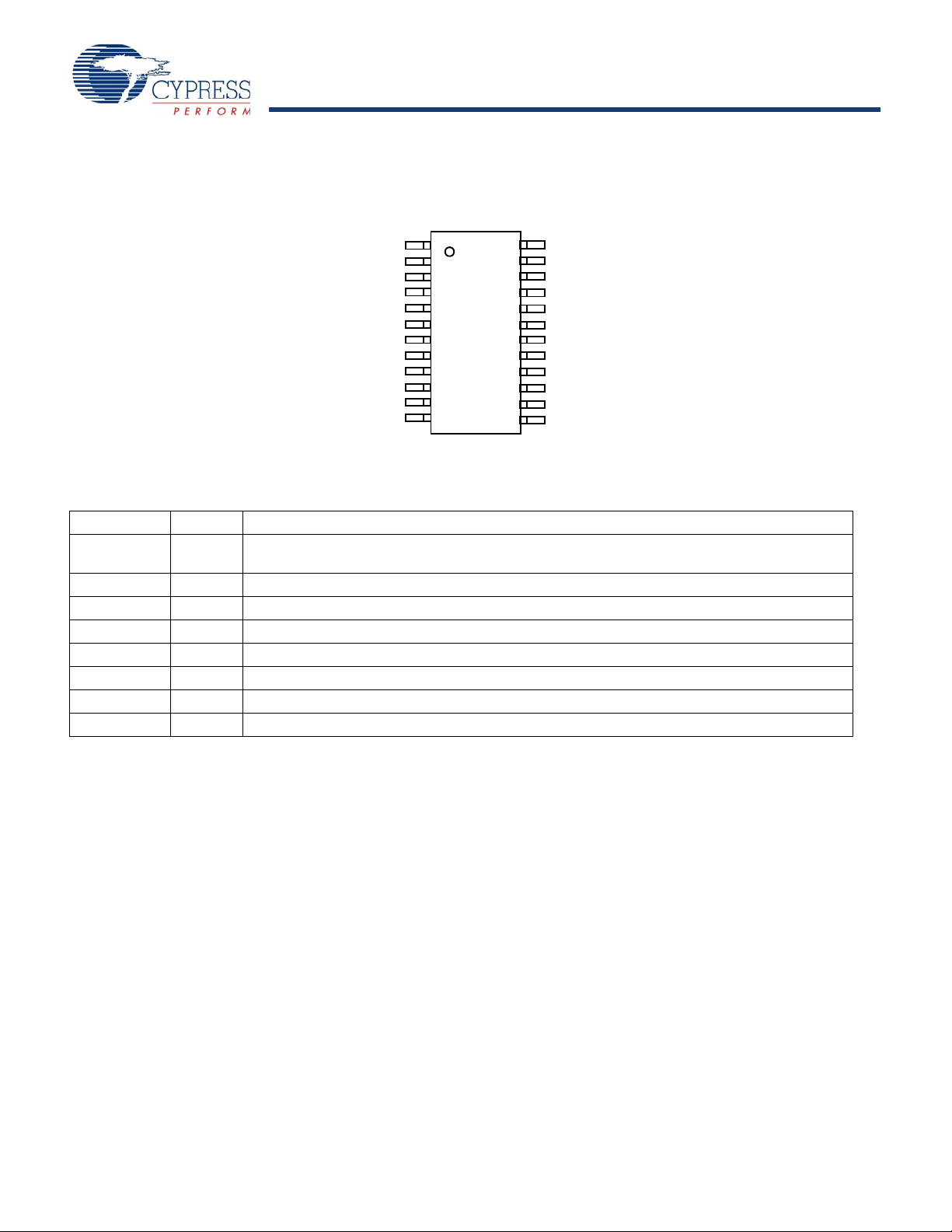
Pin Configuration
Q4
Q2
REF
V
CCQ
FS
NC
V
CCQ
V
CCN
Q0
Q1
GND
Q3
V
CCN
GND
TEST
NC
GND
V
CCN
Q7
Q6
GND
Q5
V
CCN
FB
SOIC
Top View
1
2
3
4
5
6
7
8
9
10
11
12
15
16
17
18
19
20
24
23
22
21
13
14
7B9910
7B9920
Notes
1. For all three state inputs, HIGH indicates a connection to VCC, LOW indicat es a connection to GND, and MID indicates an open connection. Internal termination
circuitry holds an unconnected input to VCC/2.
2. The level to be set on FS is determined by the “normal” operating frequency (fNOM) of the VCO (see Logic Block Diagram). The frequency appear ing at the REF
and FB inputs are fNOM when the output connected to FB is undivided. The frequency of the REF and FB inputs are fNOM/X when the device is configured for a
frequency multiplication by using external division in the feedback path of value X.
3. When the FS pin is selected HIGH, the REF input must not transition upon power up until VCC reached 4.3V.
Pin Definitions
Signal Name IO Description
REF I Reference frequency input.This input supplies the frequency and timing against which all functional
variations are measured.
FB I PLL feedback input (typically connected to one of the eight outputs).
[1,2,3]
FS
TEST I Three level select. See TEST MODE.
Q[0..7] O Clock outputs.
V
CCN
V
CCQ
GND PWR Ground.
I Three level frequency range select.
PWR Power supply for output drivers.
PWR Power supply for internal circuitry.
Test Mode
The TEST input is a three level input. In normal system operation, this pin is conn ected to ground, allowing the CY7B9910 and
CY7B9920 to operate as described in Block Di agram Description. For testing purposes, any of the three level inputs can have a
removable jumper to ground or be tied LOW through a 100W resistor. This enables an external tester to change the state of these pins.
If the TEST input is forced to its MID or HIGH state, the device operates with its internal phase locked loop disconnected and input
levels supplied to REF directly control all outputs. Relative output-to-output functions are the same as in normal mode.
Document Number: 38-07135 Rev. *B Page 2 of 11
[+] Feedback [+] Feedback
Page 3
CY7B9910
CY7B9920
Maximum Ratings
Operating outside these boundaries may affect the performance
and life of the device. These user guidelines are not tested.
Storage Temperature .................................–65
Ambient Temperature with
Power Applied ............................................–55
Supply Voltage to Ground Potential................–0.5V to +7.0V
DC Input Voltage..................................... .. .....–0.5V to +7.0V
Output Current into Outputs (LOW).............................64 mA
°C to +150°C
°C to +125°C
Static Discharge Voltage............................................>2001V
(MIL-STD-883, Method 3015)
Latch Up Current.....................................................>200 mA
Operating Range
Range
Commercial 0°C to +70°C 5V ± 10%
Industrial –40°C to +85°C 5V ± 10%
Ambient
Temperature V
CC
Document Number: 38-07135 Rev. *B Page 3 of 11
[+] Feedback [+] Feedback
Page 4
CY7B9910
CY7B9920
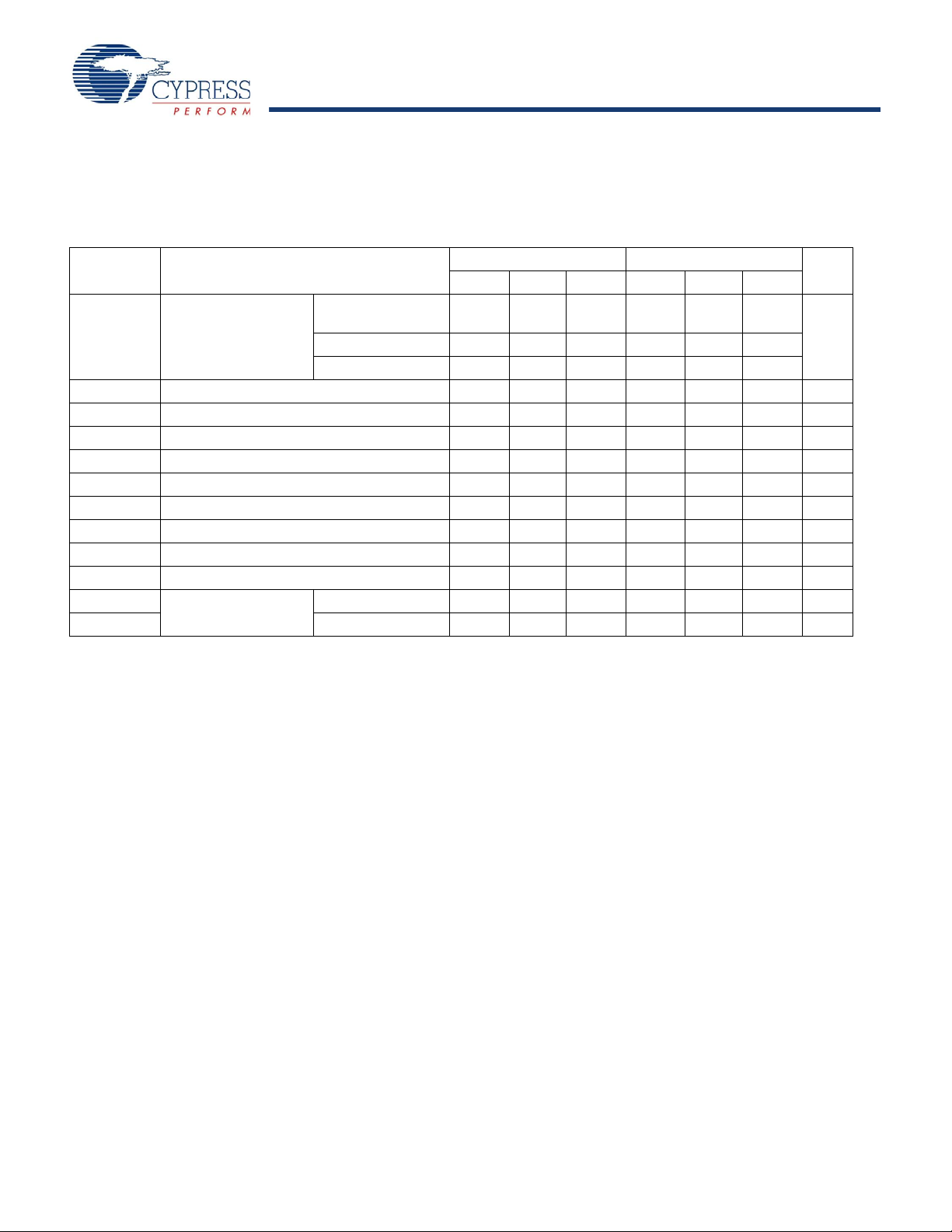
Electrical Characteristics Over the Operating Range
CY7B9910 CY7B9920
Parameter Description Test Conditions Min Max Min Max Unit
V
OH
V
OL
V
IH
V
IL
V
IHH
V
IMM
V
ILL
I
IH
I
IL
I
IHH
I
IMM
I
ILL
I
OS
I
CCQ
I
CCN
PD Power Dissipation per
Notes
4. These inputs are normally wired to VCC, GND, or left unconnected (actual threshold voltages vary as a percentage of VCC). Internal termination resistors hold
unconnected inputs at VCC/2. If these inputs are switched, the function and timing of the outputs may glitch and the PLL may require an additional tLOCK time
before all data sheet limits are achieved.
5. Te sted one output at a time, output shorted for less than one second, less than 10% duty cycle. Room temperature only. CY7B9920 outputs are not short circuit
protected.
6. To tal output current per output pair is approximated by the following expression that includes device current plus load current:
CY7B9910:
ICCN = [(4 + 0.11F) + [((835 – 3F)/Z) + (.0022FC)]N] x 1.1
CY7B9920:
ICCN = [(3.5+.17F) + [((1160 – 2.8 F) /Z) + (.0025FC)]N] x 1.1
Where
F = frequency in MHz
C = capacitive load in pF
Z = line impedance in ohms
N = number of loaded outputs; 0, 1, or 2
FC = F < C.
7. To tal power dissipation per output p air is approximated by the following expression that includ es device power dissipation plus power dissipa tion due to the load circuit:
CY7B9910:
PD = [(22 + 0.61F) + [((1550 – 2.7F)/Z) + (.0125FC)]N] x 1.1
CY7B9920:
PD = [(19.25+ 0.94F) + [((700 + 6F)/Z) + (.017FC)]N] x 1.1.See note 3 for variable definition.
Output HIGH Volt age VCC = Min, IOH = –16 mA 2.4 V
VCC = Min, IOH =–40 mA VCC–0.75
Output LOW Voltage VCC = Min, IOL = 46 mA 0.45 V
VCC = Min, IOL = 46 mA 0.45
Input HIGH Voltage
(REF and FB inputs only)
Input LOW Voltage
2.0 V
CC
VCC –
1.35
V
CC
–0.5 0.8 –0.5 1.35 V
(REF and FB inputs only)
Three Level Input HIGH
Voltage (Test, FS)
Three Level Input MID
Voltage (Test, FS)
Three Level Input LOW
Voltage (Test, FS)
[4]
[4]
[4]
Input HIGH Leakage Current
Min ≤ VCC ≤ Max VCC – 1V V
Min ≤ VCC ≤ Max VCC/2 –
500 mV
VCC/2 +
500 mV
CC
VCC – 1V V
VCC/2 –
500 mV
VCC/2 +
500 mV
CC
Min ≤ VCC ≤ Max 0.0 1.0 0.0 1.0 V
VCC = Max, VIN = Max 10 10 μA
(REF and FB inputs only)
Input LOW Leakage Current
VCC = Max, VIN = 0.4V –500 –500 μA
(REF and FB inputs only)
Input HIGH Current
(Test, FS)
Input MID Current
VIN = V
CC
200 200 μA
VIN = VCC/2 –50 50 –50 50 μA
(Test, FS)
Input LOW Current
VIN = GND –200 –200 μA
(Test, FS)
Output Short Circuit
[5]
Current
Operating Current Used by
Internal Circuitry
Output Buffer Current per
Output Pair
Output Pair
[6]
[7]
VCC = Max, V
= GND (25
V
= V
CCN
Input
OUT
°C only)
= Max All
CCQ
Selects Open
V
= V
= V
CCQ
CCQ
= Max
= Max
CCN
= 0 mA
I
OUT
Input Selects Open, f
V
CCN
I
= 0 mA
OUT
Input Selects Open, f
–250 N/A mA
Com’l 85 85 mA
Mil/Ind 90 90
14 19 mA
MAX
78 104
MAX
[5]
V
V
V
mW
Document Number: 38-07135 Rev. *B Page 4 of 11
[+] Feedback [+] Feedback
Page 5
CY7B9910
CY7B9920
Capacitance
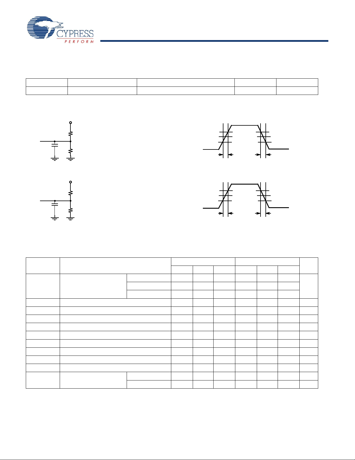
7B9910–3
7B9910–4
TTL AC Test Load (CY7B9910) TTL Input Test Waveform (Cy7B9910)
5V
R1
R2
C
L
R1
R2
C
L
7B9910–5
CMOS AC Test Load (CY7B9920)
3.0V
2.0V
V
th
=1.5V
0.8V
0.0V
≤1ns
≤1ns
2.0V
0.8V
V
th
=1.5V
80%
V
th=VCC
/2
20%
0.0V
≤ 3ns
≤ 3ns
80%
20%
V
th=VCC
/2
7B9910–6
CMOS Input Test Waveform (CY7B9920)
V
CC
R1=130
R2=91
C
L
=50pF(CL= 30pF for –5 and –2 devices)
(Includes fixture and probe capacitance)
R1=100
R2=100
C
L
=50pF(CL=30 pF for –5 and –2devices)
(Includes fixture and probe capacitance)
V
CC
Tested initially and after any design or process chan ges that may affect these parameters.
Parameter Description Test Conditions Max Unit
C
IN
Input Capacitance TA = 25°C, f = 1 MHz, VCC = 5.0V 10 pF
AC Test Loads and Waveforms
Switching Characteristics
Over the Operating Range
Parameter Description Min Typ Max Min Typ Max Unit
f
NOM
t
RPWH
t
RPWL
t
SKEW
t
DEV
t
PD
t
ODCV
t
ORISE
t
OFALL
t
LOCK
t
JR
Operating Clock
Frequency in MHz
REF Pulse Width HIGH 5.0 5.0 ns
REF Pulse Width LOW 5.0 5.0 ns
Zero Output Skew (All Outputs)
Device-to-Device Skew
Propagation Delay, REF Rise to FB Rise –0.25 0.0 +0.25 –0.25 0.0 +0.25 ns
Output Duty Cycle Variation
Output Rise Time
Output Fall Time
PLL Lock Time
Cycle-to-Cycle Output Jitter Peak to Peak 200 200 ps
Document Number: 38-07135 Rev. *B Page 5 of 11
[11]
FS = LOW
FS = MID
[1, 2]
FS = HIGH
[13, 14]
[14, 15]
[16]
[17, 18]
[17, 18]
[19]
RMS 25 25 ps
[1, 2]
[1, 2, 3]
CY7B9910–2
[8]
CY7B9920–2
15 30 15 30 MHz
25 50 25 50
40 80 40 80
0.1 0.25 0.1 0.25 ns
0.75 0.75 ns
–0.65 0.0 +0.65 –0.65 0.0 +0.65 ns
0.15 1.0 1.2 0.5 2.0 2.5 ns
0.15 1.0 1.2 0.5 2.0 2.5 ns
0.5 0.5 ms
[8]
[12]
[+] Feedback [+] Feedback
Page 6

CY7B9910
CY7B9920
CY7B9910–5 CY7B9920–5
Notes
8. Guaranteed by statistical correlation. Tested initially and after any design or process changes that may affect these parameters.
9. CMOS output buffer current and power dissipation specified at 50 MHz reference frequency.
10.Applies to REF and FB inputs only.
11.Test measurement levels for the CY7B9910 are TTL levels (1.5V to 1.5V). Test measurement levels for the CY7B9920 are CMOS levels (VCC/2 to VCC/2). T est
conditions assume signal transition times of 2ns or less and output loading as shown in the AC Test Loads and Waveforms unless otherwise specified.
12.Except as noted, all CY7B9920–2 and –5 timing parameters are specified to 80 MHz with a 30 pF load.
13.tSKEW is defined as the time between the earliest and the latest output transition among all outputs when all are loaded with 50 pF and terminated with 50Ω to
2.06V (CY7B9910) or VCC/2 (CY7B9920).
14.tSKEW is defined as the skew between outputs.
15.tDEV is the output-to-output skew between any two outputs on separate devices operating under the same cond itions (VCC, ambien t temper ature, air flow, and
so on).
16.tODCV is the deviation of the output from a 50% duty cycle.
17.Specified with outputs loaded with 30 pF for the CY7B99X0–2 and –5 de vi ce s and 5 0 pF f or the CY7B9 9X0–7 devices. Devices are terminated through 50Ω to
2.06V (CY7B9910) or VCC/2 (CY7B9920).
18.tORISE and tOFALL measured between 0.8V and 2.0V for the CY7B9910 or 0.8VCC and 0.2VCC for the CY7B9920.
19.tLOCK is the time that is required before synchronization is achieved. This specification is valid only after VCC is st able and within normal operati ng limit s. This
parameter is measured from the application of a new signal or frequency at REF or FB until tPD is within specified limits.
Parameter Description Min Typ Max Min Typ Max Unit
f
NOM
t
RPWH
t
RPWL
t
SKEW
t
DEV
t
PD
t
ODCV
t
ORISE
t
OFALL
t
LOCK
t
JR
Operating Clock
Frequency in MHz
FS = LOW
FS = MID
FS = HIGH
REF Pulse Width HIGH 5.0 5.0 ns
REF Pulse Width LOW 5.0 5.0 ns
Zero Output Skew (All Outputs)
Device-to-Device Skew
[8, 1 5 ]
[13, 14]
Propagation Delay, REF Rise to FB Rise –0.5 0.0 +0.5 –0.5 0.0 +0.5 ns
Output Duty Cycle Variation
Output Rise Time
Output Fall Time
PLL Lock Time
[17, 18
[17, 18]
[19]
[16]
Cycle-to-Cycle Output Jitter Peak to Peak
RMS
[1, 2]
[1, 2]
[1, 2, 3]
15 30 15 30 MHz
25 50 25 50
40 80 40 80
[12]
0.25 0.5 0.25 0.5 ns
1.0 1.0 ns
–1.0 0.0 +1.0 –1.0 0.0 +1.0 ns
0.15 1.0 1.5 0.5 2.0 3.0 ns
0.15 1.0 1.5 0.5 2.0 3.0 ns
0.5 0.5 ms
[8]
[8]
200 200 ps
25 25 ps
Document Number: 38-07135 Rev. *B Page 6 of 11
[+] Feedback [+] Feedback
Page 7
CY7B9910
CY7B9920
Switching Characteristics
Over the Operating Range
Parameter Description Min Typ Max Min Typ Max Unit
f
NOM
t
RPWH
t
RPWL
t
SKEW
t
DEV
t
PD
t
ODCV
t
ORISE
t
OFALL
t
LOCK
t
JR
t
JR
Operating Clock
Frequency in MHz
REF Pulse Width HIGH 5.0 5.0 ns
REF Pulse Width LOW 5.0 5.0 ns
Zero Output Skew (All Outputs)
Device-to-Device Skew
Propagation Delay, REF Rise to FB Rise –0.7 0.0 +0.7 –0.7 0.0 +0.7 ns
Output Duty Cycle Variat ion
Output Rise Time
Output Fall Time
PLL Lock Time
Cycle-to-Cycle Output
Jitter
[11]
(continued)
[19]
[17, 18]
17, 18]
FS = LOW
FS = MID
FS = HIGH
[13, 14]
[8, 15]
[16]
Peak to Peak
[8]
RMS
[1, 2]
[1, 2]
1, 2, 3]
[8]
CY7B9910–7 CY7B9920–7
15 30 15 30 MHz
25 50 25 50
40 80 40 80
[12]
0.3 0.75 0.3 0.75 ns
1.5 1.5 ns
–1.2 0.0 +1.2 –1.2 0.0 +1.2 ns
0.15 1.5 2.5 0.5 3.0 5.0 ns
0.15 1.5 2.5 0.5 3.0 5.0 ns
0.5 0.5 ms
200 200 ps
25 25 ps
Document Number: 38-07135 Rev. *B Page 7 of 11
[+] Feedback [+] Feedback
Page 8
CY7B9910
CY7B9920
AC Timing Diagrams
t
ODCV
t
ODCV
t
REF
REF
FB
Q
OTHER
Q
t
RPWH
t
RPWL
t
PD
t
SKEW
t
SKEW
t
JR
SYSTEM
CLOCK
FB
REF
FS
Q0
Q1
Q2
Q3
Q4
Q5
Q6
Q7
TEST
Z
0
LOAD
LOAD
LOAD
LOAD
REF
Z
0
Z
0
Z
0
Figure 1. AC Timing Diagrams
Figure 2. Zero Skew and Zero Delay Clock Driver
Document Number: 38-07135 Rev. *B Page 8 of 11
[+] Feedback [+] Feedback
Page 9

CY7B9910
CY7B9920
Operational Mode Descriptions
SYSTEM
CLOCK
Z
0
FB
REF
FS
TEST
REF
REF
FS
FB
LOAD
LOAD
LOAD
LOAD
LOAD
TEST
Z
0
Z
0
Z
0
Q0
Q1
Q2
Q3
Q4
Q5
Q6
Q7
Q0
Q1
Q2
Q3
Q4
Q5
Q6
Q7
Figure 2 shows the device configured as a zero skew clock
buffer. In this mode the 7B9910/9920 is used as the basis for a
low skew clock distribution tree. The outputs are aligned and may
each drive a terminated transmission line to an independent
load. The FB input is tied to any output and the operating
frequency range is selected with the FS pin. The low skew specification, coupled with the ability to drive terminated transmission
lines (with impedances as low as 50 ohms), enables efficient
printed circuit board design.
Figure 3. Board-to-Board Clock Distribution
Figure 1 shows the CY7B9910/9920 connected in series to
construct a zero skew clock distribution tree between boards.
Cascaded clock buffers accumulates low frequency jitter
because of the non-ideal filtering characteristics of the PLL filter.
Do not connect more than two clock buffers in series.
Document Number: 38-07135 Rev. *B Page 9 of 11
[+] Feedback [+] Feedback
Page 10
CY7B9910
CY7B9920
Ordering Information
51-85025-*C
Note
20.Not recommended for new design.
Accuracy
(ps)
250 CY7B9910–2SC 24-Pb Small Outline IC Commercial
500 CY7B9910–5SC 24-Pb Small Outline IC Commercial
750 CY7B9910–7SC 24-Pb Small Outline IC Commercial
Pb-Free
250 CY7B9910–2SXC 24-Pb Small Outline IC Commercial
500 CY7B9910–5SXC 24-Pb Small Outline IC Commercial
750 CY7B9910–7SXC 24-Pb Small Outline IC Commercial
Ordering Code Package Type
CY7B9910–2SCT 24-Pb Small Outline IC - Tape and Reel Commercial
CY7B9920–2SC
CY7B9910–5SCT 24-Pb Small Outline IC - Tape and Reel Commercial
CY7B9910–5SI 24-Pb Small Outline IC Industrial
CY7B9910–5SIT 24-Pb Small Outline IC - Tape and Reel Industrial
CY7B9920–5SC 24-Pb Small Outline IC Commercial
CY7B9920–5SCT 24-Pb Small Outline IC - Tape and Reel Commercial
CY7B9920–5SI 24-Pb Small Outline IC Industrial
CY7B9910–7SI
CY7B9920–7SC
CY7B9920–7SI
CY7B9910–2SXCT 24-Pb Small Outline IC - Tape and Reel Commercial
CY7B9910–5SXCT 24-Pb Small Outline IC - Tape and Reel Commercial
CY7B9910–5SXI 24-Pb Small Outline IC Industrial
CY7B9910–5SXIT 24-Pb Small Outline IC - Tape and Reel Industrial
CY7B9910–7SXCT 24-Pb Small Outline IC - Tape and Reel Commercial
[20]
[20]
[20]
[20]
24-Pb Small Outline IC Commercial
24-Pb Small Outline IC Industrial
24-Pb Small Outline IC Commercial
24-Pb Small Outline IC Industrial
Operating
Range
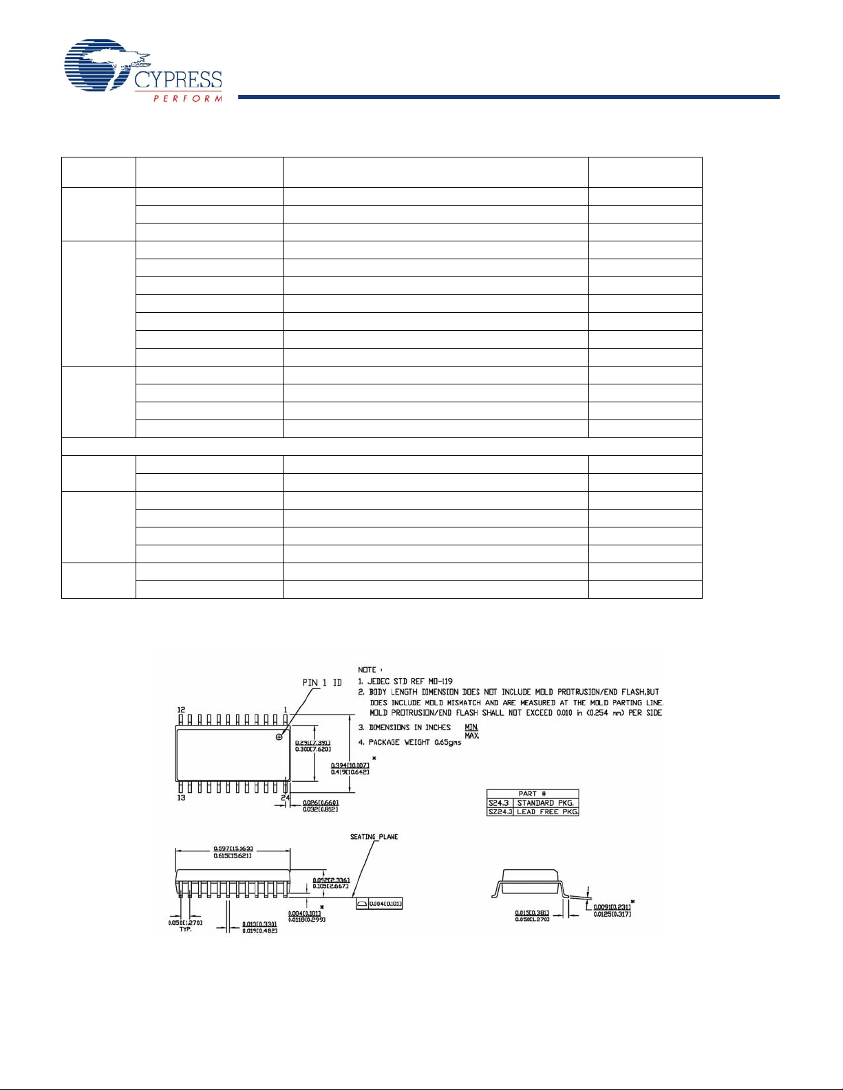
Package Diagram
Figure 4. 24-Pin (300 Mil) Molded SOIC S13
Document Number: 38-07135 Rev. *B Page 10 of 11
[+] Feedback [+] Feedback
Page 11
CY7B9910
CY7B9920
Document History
Document Title: CY7B9910/CY7B9920 Low Skew Clock Buffer
Document Number: 38-07135
REV. ECN NO. Issue Date
** 110244 10/28/01 SZV Change from Specification number: 38-00437 to 38-07135
*A 1199925 See ECN DPF/AESA Added Pb-free parts in Ordering Information
*B 1353343 See ECN AESA Change status to final
Orig. of
Change
Description of Change
Added Note 20: Not recommended for the new design
© Cypress Semiconductor Corporatio n, 20 01- 2 007 .The i n for m ation contained herein is subje ct to change without notice. Cypress Semiconductor Corporation assumes no responsibility for the use of
any circuitry other than circuitry embodied in a Cypress product. Nor does it convey or imply any license under patent or other rights. Cypress products are not warranted nor intended to be used fo r
medical, life support, life saving, critica l contr o l or safety applications, unless pursuant to a n exp ress wr i tte n ag re em en t w it h C ypr ess. Fu rth erm ore, Cyp ress doe s not auth ori ze i t s pr o ducts for use as
critical components in life-support systems where a malfunction or fa ilure may reasonably be expe cted to result in significa nt injury to the us er . The inclu sion of Cypress p roducts in life -support systems
application implies that the manufacturer assumes all risk of such use and in doing so indemnifies Cypress against all charges.
Any Source Code (software and/or firmware) is owned by Cypress Semiconductor Corporation (Cypress) and is protected by and subject to worldwide patent protection (United States and foreign),
United States copyright laws and international treaty provisions. Cypress hereby gr ant s to l icense e a pers onal, no n-exclu sive , non-tr ansfer able license to copy, use, modify, create derivative works of,
and compile the Cypress Source Code and derivative works for the sole purpose of creating custom software and or firmware in support of licensee product to be used only in conjunctio n with a Cypress
integrated circuit as specified in the ap plicable agreem ent. Any reprod uction, modificatio n, translation, co mpilation, or repr esentation of this Source Co de except as speci fied above is pro hibited with out
the express written permission of Cypress.
Disclaimer: CYPRESS MAKES NO WARRANTY OF ANY KIND, EXPRESS OR IMPLIED, WITH REGARD TO THIS MATERIAL, INCLUDING, BUT NOT LIMITED TO, THE IMPLIED WARRANTIES
OF MERCHANTABILITY AND FITNESS FOR A PARTICULAR PURPOSE. Cypress reserves the right to make changes without further notice to the materials described herein. Cypress does not
assume any liability arising out of the applic ation or use o f any pr oduct or circ uit de scribed herein . Cypr ess does n ot author ize its p roducts fo r use as critical compon ents in life-su pport systems whe re
a malfunction or failure may reason ably be expected to result in significant injury to the user. The inclusion of Cypress’ product in a life-support systems application implies that the manufacturer
assumes all risk of such use and in doing so indemnifies Cypress against all charges.
Use may be limited by and subject to the applicable Cypress software license agreement.
Document Number: 38-07135 Rev. *B Revised August 07, 2007 Page 11 of 11
PSoC Designer™, Programmable System-on-Chip™, and PSoC Express™ are trademarks and PSoC® is a registered t rade mark of Cypress S em ic on duct or C orp. A ll other trademarks or registered
trademarks referenced he rein are property of the re spective c orporatio ns. Purch ase of I2C components from Cypress or one of its sublicensed Associated Companies conveys a license under the
Philips I2C Patent Rights to use these components in an I2C system, provided that the system conforms to the I2C Standard Specification as defined by Philips. All products and company names
mentioned in this document may be the trademarks of their respective holders.
[+] Feedback [+] Feedback
 Loading...