

lock+
查询CY7B923-JXI供应商
CY7B9911
RoboClock+
Programmable Skew Clock Buffer (PSCB)
Features
tions. This multiple-out put clock dri ver provide s the system integrator with functions necessary to optimize the timing of
• All output pair skew <100 ps typical (250 max.)
• 3.75- to 100-MHz output operation
• User-selectable output functions
—Selectable skew to 18 ns
—Inverted and non-inverted
—Operation at ½ and ¼ input frequency
—Operation at 2x and 4x in put frequency (input as low
as 3.75 MHz)
• Zero input to output delay
• 50% duty-cycle outputs
• Outputs drive 50Ω terminated lines
• Low operating current
• 32-pin PLCC/LCC package
• Jitter < 200 ps peak-to-peak (< 25 ps RMS)
• Compatible with a Pentium™-based processor
Functional Description
high-performance computer systems. Eight individual TTL
drivers, arranged as four pairs of user-controllable outputs,
can each drive termin ated transmissio n lines with impedan ces
as low as 50Ω while delivering minimal and specified output skews
and full-swing logic levels.
Each output can be h ard wired to one of nine delay o r function
configurations. Delay increments of 0.6 to 1.5 ns are determined by the operating frequency with outputs able to s kew up
to ±6 time units from their nominal “zero” skew position. The completely integrated PLL allows external load a nd transmission line
delay effects to be canceled. When this “zero delay” capability of the
PSCB is combined with the selectable output skew functions, the
user can create output-to-output delays of up to ±12 time units.
Divide-by-two and divide-by-four output functions are provided
for additional flexibility in designing complex clock systems.
When combined with the internal PLL, these divide functions
allow distribution of a low-frequency clock that can be multiplied by two or four at the clock destination. This facility minimizes clock d istributi on dif ficul ty while al lowing maximu m system clock speed and flexibility.
The CY7B991 1 High Speed Programma ble Skew Clock Buffer
(PSCB) offers user-selectable control over system clock func-
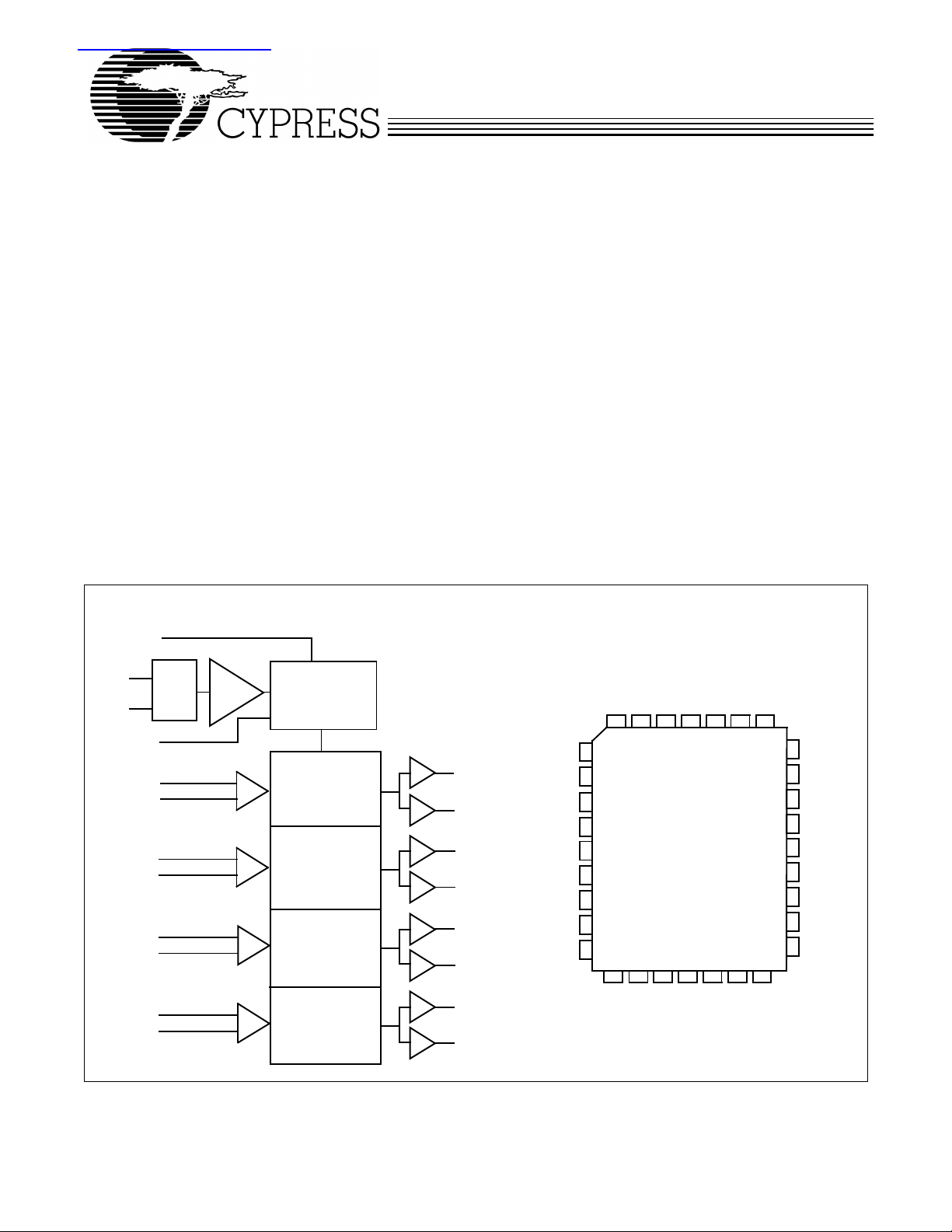
Logic Block Diagram Pin Configuration
TEST
PHASE
FB
REF
FREQ
DET
FILTER
VCO AND
TIME UNIT
GENERATOR
3F0
FS
PLCC/LCC
CCQ
V
REF
GND
TEST
2F1
FS
4F0
4F1
3F0
3F1
2F0
2F1
1F0
1F1
SELECT
INPUTS
(THREE
LEVEL)
SKEW
SELECT
MATRIX
7B9911–1
4Q0
4Q1
3Q0
3Q1
2Q0
2Q1
1Q0
1Q1
3F1
4F0
4F1
V
CCQ
V
CCN
4Q1
4Q0
GND
GND
5
6
7
8
9
10
11
12
13
3Q1
1234323130
CY7B9911
17161514 18 19 20
FB
CCNVCCN
3Q0
2Q1
V
2F0
29
28
GND
27
1F1
26
1F0
25
V
CCN
24
1Q0
23
1Q1
22
GND
GND
21
2Q0
7B9911–2
Pentium is a trademark of Intel Corporation.
Cypress Semiconductor Corporation • 3901 North First Street • San Jose • CA 95134 • 408-943-2600
Document #: 38-07209 Rev. ** Revised September 26, 2001
CY7B9911
RoboClock+
Pin Definitions
Signal
Name I/O Description
REF I Reference frequency input. This input supplies the frequency and timing against which all function al
variatio n is measured.
FB I PLL feedback input (typically connected to one of the eight outputs).
FS I Three-level frequency range select. See Table 1.
1F0, 1F1 I Three-level function select inputs for output pair 1 (1Q0, 1Q1). See Table 2.
2F0, 2F1 I Three-level function select inputs for output pair 2 (2Q0, 2Q1). See Table 2
3F0, 3F1 I Three-level function select inputs for output pair 3 (3Q0, 3Q1). See Table 2
4F0, 4F1 I Three-level function select inputs for output pair 4 (4Q0, 4Q1). See Table 2
TEST I Three-level select. See test mode section under the block diagram descriptions.
1Q0, 1Q1 O Output pair 1. See Table 2.
2Q0, 2Q1 O Output pair 2. See Table 2.
3Q0, 3Q1 O Output pair 3. See Table 2.
4Q0, 4Q1 O Output pair 4. See Table 2.
V
CCN
V
CCQ
GND PWR Ground.
PWR Power supply for output drivers.
PWR Power supply for internal circuitry.
Block Diagram Description
Phase Frequency Detector and Filter
These two blocks accept inputs from the reference frequency
(REF) input and the fe edbac k (FB) i nput a nd gen erate c orrection information to control the frequency of the Voltage-Controlled Oscillator (VCO). These blocks, along with the VCO,
form a Phase-Locked Loop (PLL) that tracks the incoming
REF signal.
VCO and Time Unit Generator
The VCO accepts analog control inputs from the PLL filter
block and generates a frequency that is used by the time unit
generator to create di sc rete time units that are sele cte d i n th e
skew select matrix. The operational range of the VCO is determined by the FS control pin. The time unit (t
by the operating frequency of the device and the level of the
FS pin as shown in Table 1.
Table 1. Frequency Range Select and tU Calculation
f
(MHz)
FS
NOM
U
[2, 3]
1
----------------------- -
=
f
NOM
where N =
N×
LOW 15 30 44 22.7
MID 25 50 26 38.5
HIGH 40 100 16 62.5
Skew Select Matrix
The skew select ma trix is c om pri se d of fo ur independent sections. Each section has two low-skew, high-fanout drivers
(xQ0, xQ1), and tw o c orre sp ond ing t hree - lev el f unc tio n se lec t
) is determined
U
[1]
Approximate
Frequency (MHz) At
Which tU = 1.0 nsMin. Max.
(xF0, xF1) inputs. Table 2 below shows the nine possible out-
put functions for each section as determined by the function
select inputs. All times are measured with respect to the REF
input assuming that the output connected to the FB input has
selected.
0t
U
Table 2. Programmable Skew Configurations
[1]
Function Selects Output Functions
1F1, 2F1,
3F1, 4F1
LOW LOW –4t
LOW MID –3t
LOW HIGH –2t
MID LOW –1t
MID MID 0t
MID HIGH +1t
HIGH LOW +2t
HIGH MID +3t
HIGH HIGH +4t
Notes:
1. For all three-state inputs, HIGH indicates a connection to V
2. The level to be set on FS is determined by the “normal” operating fre-
3. When the FS pin is selected HIGH, the REF input must not transition
1F0, 2F0,
3F0, 4F0
indicates a connection to GND, and MID indicates an open connection.
Internal termination circuitry holds an unconnected input to V
quency (f
Diagram). Nominal frequency (f
other outputs when they are operated in their undivided modes (see
Table 2). The frequency appearing at the REF and FB inputs will be f
when the output connected to FB is undivided. The frequency of the REF
and FB inputs will be f
frequency multiplication by using a divided output as the FB input.
upon power-up until V
) of the VCO and Time Unit Generator (see Logic Block
NOM
1Q0, 1Q1,
2Q0, 2Q1 3Q0, 3Q1 4Q0, 4Q1
Divide by 2 Divide by 2
U
U
U
U
U
U
U
U
U
NOM
/2 or f
NOM
CC
NOM
has reached 4.3V.
–6t
U
–4t
U
–2t
U
0t
U
+2t
U
+4t
U
+6t
U
Divide by 4 Inverted
) always appears at 1Q0 and the
/4 when the part is configured for a
–6t
–4t
–2t
+2t
+4t
+6t
CC
CC
U
U
U
0t
U
U
U
U
, LOW
/2.
NOM
Document #: 38-07209 Rev. ** Page 2 of 12
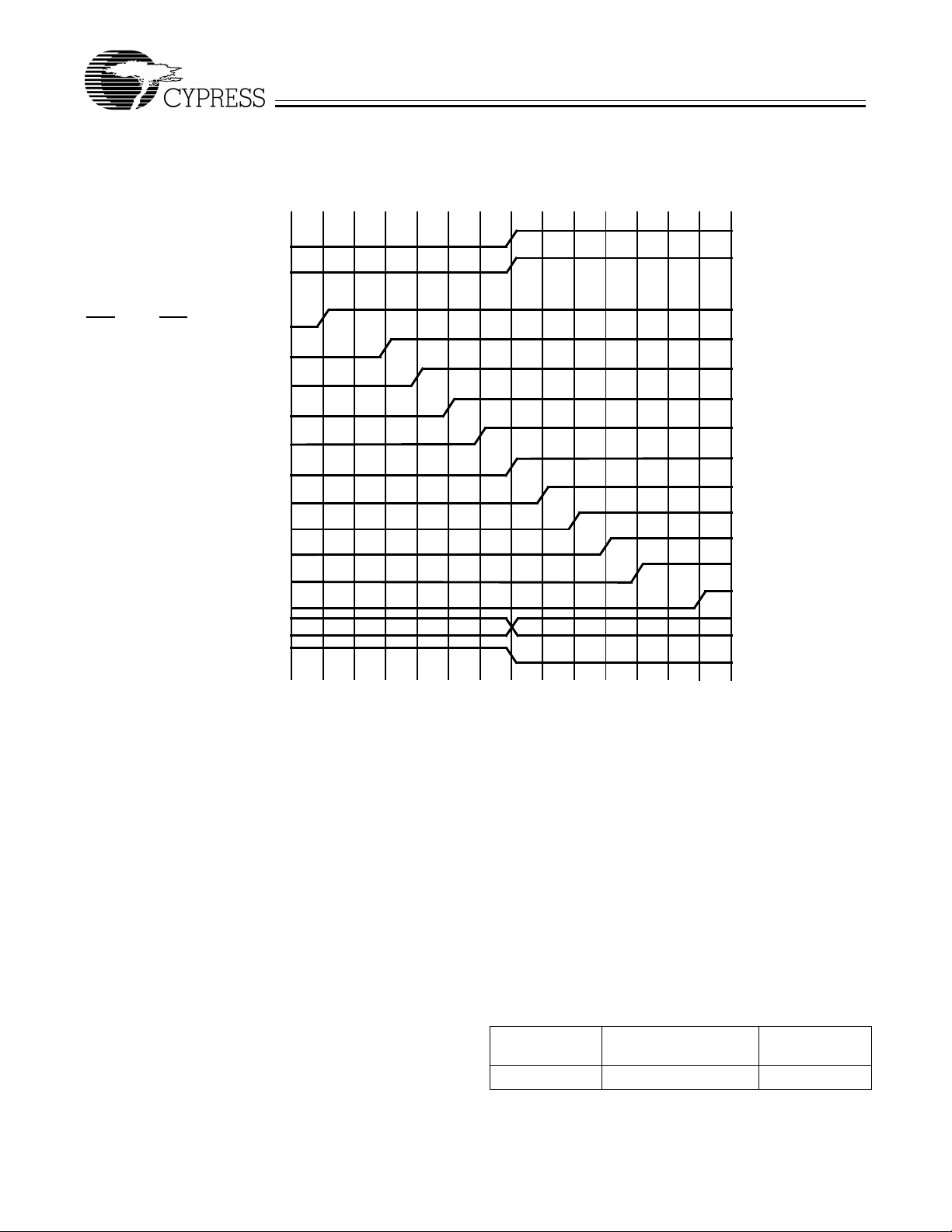
1Fx
2Fx
(N/A)
3Fx
4Fx
LM
FB Input
REF Input
– 6t
CY7B9911
RoboClock+
U
U
U
U
U
U
– 6t
– 5t
– 4t
– 3t
– 2t
0
0
0
t
t
U
0
t
t
– 1t
0
0
t
t
t 0t
U
+1t
+2tU+3tU+4tU+5tU+6t
0
t 0t 0t 0t 0t
U
0
LL
LM
LH
ML
MM
MH
HL
HM
HH
(N/A)
(N/A)
(N/A)
LH
(N/A)
ML
(N/A)
MM
(N/A)
MH
(N/A)
HL
HM
LL/HH
HH
– 4t
– 3t
– 2t
– 1t
0t
+1t
+2t
+3t
+4t
+6t
DIVIDED
INVERT
U
U
U
U
U
U
U
U
U
U
Figure 1. Typical Outputs with FB Connected to a Zero-Skew Output
Test Mode
The TEST input is a three-level input. In normal system operation, this pin i s con nec ted to ground, allowing the C Y7B9 911
to operate as explained briefly above (for testing purposes,
any of the three-level inputs can have a removable jumper to
ground, or be tied LOW through a 10 0Ω resistor. This will allow
an external tester to change the state of these pins.)
If the TEST input is forced to its MID or HI GH sta te, the dev ice
will operate with its internal phase locked loop disconnected,
and input levels s upplied to REF w ill directly control a ll outputs.
Relative output to output functions are the same as in normal
mode.
In contrast with normal operatio n (TEST tied LOW). All outputs
will function base d only on the conn ection of their own f unction
select inputs (xF0 and xF1) and the waveform characteristics
of the REF input.
7B9911–3
[4]
Maximum Ratings
(Above which the usefu l l ife may be impaired. For us er g uid elines, not tested.)
Storage Temperature .................................–65
°C to +150°C
Ambient Temper atu re with
Power Applied............................................–55
°C to +125°C
Supply Voltage to Ground Potential ...............–0.5V to +7.0V
DC Input Voltage............................................–0.5V to +7.0V
Output Current into Outputs (LOW).............................64 mA
Static Discharge Voltage...........................................>2001V
(per MIL-STD-883, Method 3015)
Latch-Up Current.....................................................>200 mA
Operating Range
Range
Temperature V
CC
Commercial 0°C to +70°C 5V ± 10%
Ambient
Note:
4. FB connected to an output selected for “zero” skew (i.e., xF1 = xF0 =
MID).
Document #: 38-07209 Rev. ** Page 3 of 12
CY7B9911
RoboClock+
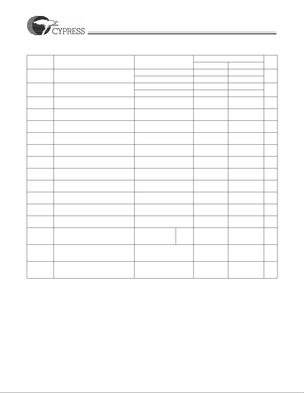
Electrical Characteristics Ov er the Op erat ing Range
CY7B9911
Parameter Description Test Conditions Min. Max. Unit
V
OH
V
OL
V
IH
V
IL
V
IHH
V
IMM
V
ILL
I
IH
I
IL
I
IHH
I
IMM
I
ILL
I
OS
I
CCQ
I
CCN
PD Power Dissipation per
Notes:
5. These inputs are normally wired to V
unconnected inputs at V
before all datasheet limits are achieved.
6. CY7B9911 should be tested one output at a time, output shorted for less than one second, less than 10% duty cycle. Room temperature only.
7. Total output current per output pair can be approximated by the following expression that includes device current plus load current:
CY7B9911: I
Where
8. T otal power dissipation per output pair can be approximated by the following expression that includes device power dissipation plus power di s si pa t ion d u e to
the load circuit:
CY7B9911: PD = [(22 + 0.61F) + [((1550 – 2.7F)/Z) + (.0125FC)]N] x 1.1
See note 7 for variable definition.
Output HIGH Voltage VCC = Min., IOH = –16 mA 2.4 V
VCC = Min., IOH =–40 mA
Output LOW Voltage VCC = Min., IOL = 46 mA 0.45 V
VCC = Min., IOL = 46 mA
Input HIGH Voltage
(REF and FB inputs only)
Input LOW Voltage
2.0 V
CC
–0.5 0.8 V
(REF and FB inputs only)
Three-Level Input HIGH
Voltage (Test, FS, xFn)
Three-Level Input MID
Voltage (Test, FS, xFn)
Three-Level Input LOW
Voltage (Test, FS, xFn)
[5]
[5]
[5]
Input HIGH Leakage Current (REF an d
Min. ≤ VCC ≤ Max. VCC – 0.85 V
CC
Min. ≤ VCC ≤ Max. VCC/2 – 500 mV VCC/2 + 500 mV V
Min. ≤ VCC ≤ Max. 0.0 0.85 V
VCC = Max., VIN = Max. 10 µA
FB inputs only)
Input LOW Leakage Cur rent (REF and
VCC = Max., VIN = 0.4V –500 µA
FB inputs only)
Input HIGH Current
(Test, FS, xFn)
Input MID Current
VIN = V
CC
200 µA
VIN = VCC/2 –50 50 µA
(Test, FS, xFn)
Input LOW Current
VIN = GND –200 µA
(Test, FS, xFn)
Output Short Circuit
[6]
Current
Operating Current Used by
Internal Circuitry
VCC = Max., V
= V
°C only)
CCQ
= GND (25
V
CCN
Max., All Input
OUT
=
–250 mA
Com’l 85 mA
Selects Open
Output Buffer Current per
Output Pair
Output Pair
= [(4 + 0.11F) + [((835 – 3F)/Z) + (.0022FC)]N] x 1.1
CCN
F = frequency in MHz
C = capacitive load in pF
Z = line impedance in ohms
N = number of loaded outputs; 0, 1, or 2
∗ C
FC = F
[7]
[8]
, GND, or left unconnected (actual threshold voltages vary as a percentage of VCC). Internal termination resistors hold
CC
/2. If these inputs are switched, the function and timing of the outputs may glitch and the PLL may require an additional t
CC
V
= V
= V
CCQ
CCQ
= Max.,
= Max.,
CCN
= 0 mA
I
OUT
Input Selects Open, f
V
CCN
= 0 mA
I
OUT
Input Selects Open, f
14 mA
MAX
78 mW
MAX
LOCK
V
V
time
Document #: 38-07209 Rev. ** Page 4 of 12

CY7B9911
RoboClock+
Capacitance
[9]
Parameter Description Test Conditions Max. Unit
C
IN
Note:
9. Applies to REF and FB inputs only. Tested initially and after any design or process changes that may affect these parameters.
Input Capacitance TA = 25°C, f = 1 MHz, VCC = 5.0V 10 pF
AC Test Loads and Waveforms
5V
R1=130
R1
R2=91
C
=30pF
C
L
L
(Includes fixture and probe capacitance)
R2
7B9911–4
2.0V
V
=1.5V
th
0.8V
0.0V
≤1ns ≤1ns
TTL ACTest Load (CY7B9911) TTL Input Test Waveform (CY7B9911)
3.0V
2.0V
V
th
0.8V
=1.5V
7B9911–5
Document #: 38-07209 Rev. ** Page 5 of 12

CY7B9911
RoboClock+
Switching Characteristics O ver the Operating Range
[2, 10, 11]
CY7B9911–5 CY7B9911–7
Parameter Description Min. Typ. Max. Min. Typ. Max. Unit
[12, 14]
[11]
[1, 2]
[1, 2]
[1, 2 , 3 ]
[18, 19]
[18, 19]
[11]
15 30 15 30 MHz
25 50 25 50
40 100 40 100
See
Table 1
Table 1
0.1 0.25 0.1 0.25 ns
0.25 0.5 0.3 0.75 ns
0.6 0.7 0.6 1.0 ns
0.5 1.2 1.0 1.7 ns
0.5 0.9 0.7 1.4 ns
0.5 1.2 1.2 1.9 ns
1.25 1.65 ns
–1.0 0.0 +1.0 –1.2 0.0 +1.2 ns
2.0 2.5 ns
2.5 3 ns
0.15 1.0 1.5 0.15 1.5 2.5 ns
0.15 1.0 1.5 0.15 1.5 2.5 ns
0.5 0.5 ms
25 25 ps
200 200 ps
f
NOM
t
RPWH
t
RPWL
t
U
t
SKEWPR
t
SKEW0
t
SKEW1
t
SKEW2
t
SKEW3
t
SKEW4
t
DEV
t
PD
t
ODCV
t
PWH
t
PWL
t
ORISE
t
OFALL
t
LOCK
t
JR
Operating Clock
Frequency in MHz
FS = LOW
FS = MID
FS = HIGH
REF Pulse Width HIGH 4.0 4.0 ns
REF Pulse Width LOW 4.0 4.0 ns
Programmable Skew Unit See
Zero Output Matched-Pair Skew
(XQ0, XQ1)
[12, 13]
Zero Output Skew (All Outputs)
Output Skew (Rise-Rise, Fall-Fall, Same
Class Outputs)
Output Skew (Rise-Fall, Nomina l-Inv ert ed,
Divided-Divided)
Output Skew (Rise-Rise, Fall-Fall, Different
Class Outputs)
Output Skew (Rise-Fall, Nominal-Divided,
Divided-Inverted)
Device-to-Device Skew
[12, 15]
[12, 15]
[12, 15]
[12, 15]
[11, 16]
Propagation Delay, REF Rise to FB Rise –0.5 0.0 +0.5 –0.7 0.0 +0.7 ns
Output Duty Cycle Variation
[17]
Output HIGH Ti me Deviati on from 50%
Output LOW Ti me De vi ati on fro m 50 %
Output Rise Time
Output Fall Time
PLL Lock Time
Cycle-to-Cycle Output
Jitter
[18, 20]
[18, 20]
[21]
RMS
Peak-to-Peak
Notes:
10. Test measurement levels for the CY7B9911 are TTL levels (1.5V to 1.5V).
Test conditions assume signal transition times of 2 ns or less and output loading
as shown in the AC Test Loads and Waveforms unless otherwise specified.
11. Guaranteed by statistical correlation. Tested initially and after any design
or process changes that may affect these parameters.
12. SKEW is defined as the time between the earliest and the latest output
transition among all outputs for which the same t
when all are loaded with 30 pF and terminated with 50
13. t
14. t
15. There are three classes of outputs: Nominal (multiple of t
is defined as the skew between a pair of outputs (XQ0 and XQ1) when
SKEWPR
all eight outputs are selected for 0t
is defined as the skew between outputs when they are selected for 0tU.
SKEW0
Other outputs are divided or inverted but not shifted.
(4Q0 and 4Q1 only with 4F0 = 4F1 = HIGH), and Divided (3Qx and 4Qx only in
Divide-by-2 or Divide-by-4 mode).
.
U
delay has been selected
U
Ω to 2.06V.
delay), Inverted
U
is the output-to-output skew between any two devices operating under the
16. t
DEV
same conditions (V
17. t
18. Specified with outputs loaded with 30 pF. Devices are terminated through
19. t
20. t
21. t
is the deviation of the output from a 50% duty cycle. Output pulse width
ODCV
variations are included in t
Ω to 2.06V.
50
is measured at 2.0V . t
PWH
and t
ORISE
is the time that is required before synchronization is achieved. This speci-
LOCK
fication is valid only after V
parameter is measured from the application of a new signal or frequency at REF
or FB until t
ambient temperature, air flow, etc.)
CC
and t
SKEW2
is measured at 0.8V.
PWL
measured between 0.8V and 2.0V.
OFALL
is stable and within normal operating limits. This
CC
is within specified limits.
PD
SKEW4
specifications.
Document #: 38-07209 Rev. ** Page 6 of 12

AC Timing Diagrams
CY7B9911
RoboClock+
REF
FB
Q
OTHERQ
INVERTED Q
REF DIVIDED BY 2
t
REF
t
RPWH
t
PD
t
SKEWPR,
t
SKEW0,1
t
SKEW3,4
t
ODCV
t
SKEW3,4
t
RPWL
t
t
SKEW2
ODCV
t
SKEWPR,
t
SKEW0,1
t
SKEW2
t
SKEW3,4
t
JR
REF DIVIDED BY 4
t
SKEW1,3, 4
t
SKEW2,4
7B9911–8
Document #: 38-07209 Rev. ** Page 7 of 12

Operational Mode Descriptions
CY7B9911
RoboClock+
REF
FB
SYSTEM
CLOCK
REF
FS
4F0
4F1
3F0
3F1
2F0
2F1
1F0
1F1
TEST
4Q0
4Q1
3Q0
3Q1
2Q0
2Q1
1Q0
1Q1
LENGTH L1 = L2 = L3 = L4
Figure 2. Zero-Skew and/or Zero-Delay Clock Driver
Figure 2 shows the PSCB configured as a zero-skew clock
buffer. In this mode the 7B9911 can be used as the basis for a
low-skew clock distri bution tree. When all of the functi on select
inputs (xF0, xF1) are left open, the outputs are aligned and
may each drive a terminated transmission line to an indepen-
REF
LOAD
Z
L1
L2
L3
L4
0
LOAD
Z
0
LOAD
Z
0
LOAD
Z
0
7B9911–9
dent load. The FB input can be tied to any output in this configuration and the operating frequency range is selected with
the FS pin. The low-sk ew specification , coupled with the ability
to drive terminated tra nsmission lines (w ith impedances a s low
as 50 ohms), allows efficient printed circuit board design.
LOAD
FB
SYS–
TEM
CLOCK
REF
FS
4F0
4F1
3F0
3F1
2F0
2F1
1F0
1F1
TEST
4Q0
4Q1
3Q0
3Q1
2Q0
2Q1
1Q0
1Q1
LENGTH L1 = L2
L3 < L2 by 6 inches
L4 > L2 by 6 inches
Figure 3. Programmable-Skew Clock Driver
Figure 3 shows a configuration to equalize skew between metal traces of different lengths. In addition to low skew between
outputs, th e PSCB can be pro gr amme d to st agg er th e ti ming
of its outputs. The four groups of output pairs can each be
programmed to different output timing. Skew timing can be
adjusted over a wide range in small increments with the appropriate strapping of the func tion select pins. In this confi guration
the 4Q0 output is fe d back to FB a nd configure d for zero skew .
The other three pairs of outputs are programmed to yield different skews relative to the feedback. By advancing the clock
signal on the longer traces or retarding the clock signal on
shorter traces, all loads can receive the clock pulse at the
same time.
Z
L1
L2
L3
L4
0
LOAD
Z
0
LOAD
Z
0
LOAD
Z
0
7B9911–10
In this illustration the FB input is connected to an output with
0-ns skew (xF1, xF0 = MID) selected. The internal PLL synchronizes the FB and REF inputs and aligns their ri sing edge s
to insure that all outputs have precise phase alignment.
Clock skews can be advanced by ±6 time units (t
an output selected for zero skew as the feedback. A wider range of
) when using
U
delays is possible if the output connected to FB is also skewed.
Since “Zero Skew”, +t
groups, and since the PLL aligns the rising edges of REF and FB,
, and –tU are defined relative to output
U
it is possible to create wider output skews by proper selection of the
xFn inputs. For example a +10 t
achieved by connecting 1Q0 to FB and setting 1F0 = 1F1 = GN D,
3F0 = MID, and 3F1 = High. (Since FB aligns at –4 t
between REF and 3Qx can be
U
and 3Qx
U
Document #: 38-07209 Rev. ** Page 8 of 12

7B9911–11
FB
REF
FS
4F0
4F1
3F0
3F1
2F0
2F1
1F0
1F1
4Q0
4Q1
3Q0
3Q1
2Q0
2Q1
1Q0
1Q1
TEST
REF
7B9911–12
FB
REF
FS
4F0
4F1
3F0
3F1
2F0
2F1
1F0
1F1
4Q0
4Q1
3Q0
3Q1
2Q0
2Q1
1Q0
1Q1
TEST
REF
20 MHz
20 MHz
40 MHz
80 MHz
CY7B9911
RoboClock+
skews to +6 tU, a total of +10 tU skew is realized.) Many other configurations can be realized by skewing both the output used as the
FB input and skewing the other outputs.
simultaneously an d are ou t of pha se on t heir ris ing ed ge. Thi s
will allow the designer to use the rising edges of the
quency and 1⁄4 frequency outputs without concern for rising-edge skew. The 2Q0, 2Q1, 1Q0, and 1Q1 outputs run at
80 MHz and are skewed by programming their select inputs
accordingly . Note that the FS pin is wired for 80-MHz operation
because that is the frequency of the fastest output.
REF
FB
REF
FS
4F0
4F1
3F0
3F1
2F0
2F1
1F0
1F1
TEST
4Q0
4Q1
3Q0
3Q1
2Q0
2Q1
1Q0
1Q1
10 MHz
5 MHz
20 MHz
Figure 6. Frequency Divider Connections
7B9911–13
Figure 4. Inverted Output Connections
Figure 4 shows an exampl e of the invert func tion of the PSCB.
In this example the 4Q0 output used as the FB input is programmed for invert (4F0 = 4F1 = HIGH) while the other three
pairs of outputs are pro grammed for zero skew . When 4F0 and
4F1 are tied high, 4Q0 and 4Q1 become inverted zero phase
outputs. The PLL alig ns the rising edge of the FB input w ith the
rising edge of the REF. This causes the 1Q, 2Q, and 3Q outputs to become the “inverted” outputs with respect to the REF
input. By selecting w hich out put is con nect to FB, i t is possibl e
to have 2 inverted and 6 non-inverted ou tputs or 6 inverted an d
2 non-inverted outp uts. The correct co nfiguration wou ld be determined by the need for more (or few er) inverted outputs . 1Q,
2Q, and 3Q ou tputs can also be skewed to com pensate for
varying trace delays independent of inversion on 4Q.
20 MHz
Figure 6 demons trates the PSCB in a clock di vider applica tion.
2Q0 is fed back to the FB input and programmed for zero skew.
3Qx is programmed to divide by four. 4Qx is programmed to
divide by two. Note that the falling edges of the 4Qx and 3Qx
outputs are aligned. This allows use of the risi ng edges of the
1
⁄2 frequency and 1⁄4 frequency without concern for s ke w mis -
match. The 1Qx outputs are programmed to zero skew and
are aligned with the 2Qx outputs. In this example, the FS input
is grounded to configur e the device in the 15- to 30-MHz range
since the highest frequency outp ut is running at 20 MHz.
Figure 7 shows some of the functions that are selectable on
the 3Qx and 4Qx output s. Thes e inclu de inv erted ou tputs an d
outputs that off er divide-by-2 and divide-by-4 timing . An inverted output allows the system designer to clock different subsystems on opposite edges, without suffering from the pulse
asymmetry typical of non-ideal loading. This function allows
the two subsystems to each be clocked 180 degrees out of
phase, but still to be aligned within the skew spec.
The divided outputs offer a zero-delay divider for portions of
the system that need the clock to be divided by either two or
four, and still rema in within a narrow s kew of the “1X” clock.
Without this feature, an external divider wou ld need to be added, and the propagation delay of the divider would add to the
skew between the different clock signals.
These divided outputs, coupled with the Phase Locked Loop,
allow the PSCB to multiply the clock rate at the REF input by
either two or four. This mode will enable the designer to dis-
Figure 5. Frequency Multiplier with Skew Connections
Figure 5 illustrates the PSCB configured as a clock multiplier.
The 3Q0 output is programmed to divide by four and is fed
back to FB. This cau ses the PLL to increase it s frequency until
the 3Q0 and 3Q1 output s are lo cked at 20 MHz while the 1Qx
and 2Qx outputs run at 80 MHz . The 4Q0 and 4Q1 outputs are
programmed to divide by two, which results in a 40-MHz waveform at these outputs. Note that the 20- and 40-MHz c locks fall
Document #: 38-07209 Rev. ** Page 9 of 12
tribute a low-frequency clock between various portions of the
system, and then locally multip ly the clock rate to a more sui table frequency, w hile still maintai ning the low-s kew c haract eristics of the cl ock driver . The PSCB c an perform all of the func tions described above at the same time. It ca n multip ly by two
and four or divide by two (and four) at the same time that it is
shifting its outpu ts over a wide range or main taining zero skew
between selected outputs.
1
⁄2 fre-

CY7B9911
RoboClock+
20–MHz
DISTRIBUTION
CLOCK
SYSTEM
CLOCK
FB
REF
FS
4F0
4F1
3F0
3F1
2F0
2F1
1F0
1F1
TEST
FB
REF
FS
4F0
4F1
3F0
3F1
2F0
2F1
1F0
1F1
TEST
REF
4Q0
4Q1
3Q0
3Q1
2Q0
2Q1
1Q0
1Q1
SKEWED4ns
Figure 7. Multi-Function Clock Driver
REF
4Q0
4Q1
3Q0
3Q1
2Q0
2Q1
1Q0
1Q1
L4
ZEROSKEW
80–MHz
L1
L2
L3
80–MHz
INVERTED
20–MHz
80–MHz
Z
0
Z
0
FB
REF
FS
4F0
4F1
3F0
3F1
2F0
2F1
1F0
1F1
TEST
LOAD
LOAD
Z
0
LOAD
Z
0
LOAD
Z
0
7B9911–14
LOAD
Z
0
LOAD
Z
0
LOAD
Z
0
4Q0
4Q1
3Q0
3Q1
2Q0
2Q1
1Q0
1Q1
LOAD
LOAD
7B9911–15
Figure 8. Board-to-Board Clock Distribution
Figure 8 shows the CY7B9911 connected in series to construct a zero-skew c lock distri bution tree between boards. Delays of the downstream clock buffers can be programmed to
compensate for the wire length (i.e., select negative skew
equal to the wire delay) nec essary to connect them to th e mas-
ter clock source, approximating a zero-delay clock tree. Cascaded clock buffers will accumulate low-frequency jitter because of the non-ideal fi ltering charac teristi cs of the PLL fi lter.
It is recommended that not more than two clock buffers be
connected in series.
Ordering Information
Accuracy
(ps) Ordering Code
500 CY7B9911–5JC J65 32-Lead Plastic Leaded Chip Carrier Commercial
750 CY7B9911–7JC J65 32-Lead Plastic Leaded Chip Carrier Commercial
Document #: 38-07209 Rev. ** Page 10 of 12
Package
Name Package Type
Operating
Range

ng so indemnifies Cypress Semiconductor against all charges.
Package Diagrams
32-Lead Plastic Leaded Chip Carri er J65
CY7B9911
RoboClock+
Document #: 38-07209 Rev. ** Page 11 of 12
© Cypress Semiconductor Corporation, 2001. The information contained herein is subject to change without notice. Cypress Semiconductor Corporation assumes no responsibility for the use
of any circuitry other than circuitry embodied in a Cypress Semiconductor product. No r does it convey or imply any license under patent or other rights. Cypress Semiconductor does not autho rize
its products for use as critical components in life-support systems where a malfunction or failure may reasonably be expected to result in significant injury to the user. The inclusion of Cypress
Semiconductor products in life-support systems application implies that the manufacturer assume s all risk of such use and in doi

Document Title: CY7B9911 RoboClock+ Programmable Skew Clock Buffer (PSCB)
Document Number: 38-07209
REV. ECN NO.
** 110342 12/21/01 SZV Change from Spec number: 38-00623 to 38-07209
Issue
Date
Orig. of
Change Description of Change
CY7B9911
RoboClock+
Document #: 38-07209 Rev. ** Page 12 of 12
 Loading...