

Page 1
,
查询CY7B923供应商
CY7B923
CY7B933
HOTLink™ Transmitter/Receiver
Features
• Fibre Ch an n e l c o m p li an t
• IBM ESCON
• DVB-ASI compliant
• ATM compliant
• 8B/10B-coded or 10-bi t unencoded
• Standard HOTLink: 160–330 Mbps
• High Speed HO TLink: 160–400 Mbps f or high spe ed applications
• Low Sp eed HOTLi nk: 15 0–160 Mbps for Lo w Cost Fib er
application s
• TTL synchronous I/O
• No external PLL components
• Triple PECL 100K serial outputs
• Dual PECL 100K serial inputs
• Low power: 350 mW (Tx), 650 mW (Rx)
• Compatibl e with fiber-opt ic modules, coaxi al cable, and
twisted pair media
• Built-In Self-Test
• Single +5V supply
• 28-pin SOIC/PLCC/LCC
0.8µ BiCMOS
•
®
compliant
Functional Description
The CY7B923 HOTLink™ T r ansmitter and CY7B933 HOTLink
Receiver are point-to-point communications building blocks
that trans fer data ov er high-s peed serial li nks (fi ber, coax, and
twisted pair). Standard HOTLink data rates range from
160-330 Mbits/second. Higher speed HOTLink is also available for high speed applications (160-400 Mbits/second), as
well as for those Low Cost applications HO TLink-155 (150-160
Mbits/second operations).
Figure 1
illustrates typical connec-
tions to host system s or controllers .
Eight bits of user data or protocol information are loaded into
the HOTLink t r ansmit ter and are e ncoded. Se rial da ta is s hift ed out of the three dif feren tial posi tive ECL (PECL) serial ports
at the bit rate (whic h is 10 t imes the byte rate).
The HOTLink receiver accepts the serial bit stream at its differenti al line re ceiver inputs an d, using a complet ely integr ated
PLL Clock Synchronizer, recovers the timing information necessary for data recons truc tion. The bit stream is deserial ized ,
decoded, and checked for transmission errors. Recovered
bytes are pres ented i n paral lel t o the rece iving host along with
a byte -r a te clock.
The 8B/10B encoder/dec oder can be di sab led in systems tha t
already encode or scramble the transmitted data. I/O signals
are available to create a seamless interface with both asynchronous FIFOs (i.e., CY7C42X) and clocked FIFOs (i.e.,
CY7C44X). A Built-In Self-Test pattern generator and checke r
allows testing of the transmitter, receiver, and the connecting
link as a part of a system diagnosti c check.
HOTLink devices are ideal for a variety of applications where
a parallel interface can be replaced with a high-speed
point-to-point serial link. Applications include interconnecting
workstations, servers, mass storage, and video transmission
equipment.
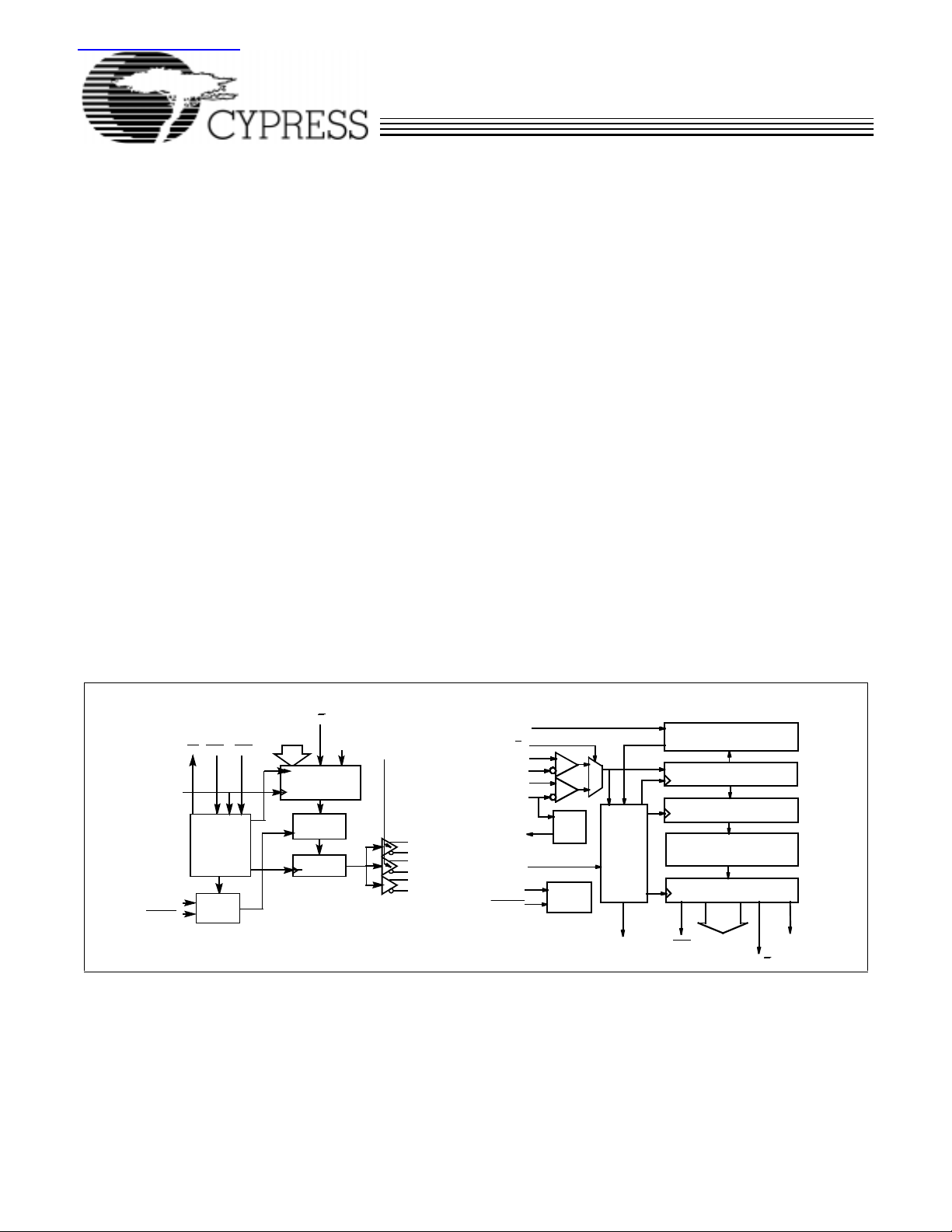
CY7B923TransmitterLogicBlock Diagram
SC/D (Da)
D
0−7
(D
)
b−h
ENAENNRP
CKW
CLOCK
GENERATOR
MODE
BISTEN
TEST
LOGIC
HOTLi nk is a trademark of cypress Semiconductor Corporation.
ESCON is a registered trademark of IBM.
SVS(Dj)
ENABLE
INPUT REGI STER
ENCODER
SHIFTER
FOTO
OUTA
OUTB
OUTC
B923–1
CY7B933ReceiverLogicBlockDiagram
A/B
INA+
INA
INB(INB+)
SI(INB−)
REFCLK
MODE
BISTEN
RF
SO
−
PECL
TTL
CLOCK
SYNC
TEST
LOGIC
CKR RDY
DATA
FRAMER
SHIFTER
DECODER
REGISTER
DECODER
OUTPUT
REGISTER
Q
0−7
(Q
)
b−h
SC/D(Qa)
RVS(Qj)
B923–2
Cypress Semiconductor Corporation
• 3901 North First Street • San Jose • CA 95134 • 408-943-2600
April 5
1999
Page 2
LOGIC
SC/D(Qa)
INA
−
INA+
A/B
BISTEN
RF
GND
RDY
GND
V
CCN
RVS(Qj)
(Q
h)Q7
(Qg)Q
6
(Qf)Q
5
(Qi)Q
4
INB(INB+)
SI(INB−)
MODE
REFCLK
V
CCQ
SO
CKR
V
CCQ
GND
SC/D(Qa)
Q
0(Qb
)
Q
2(Qd
)
Q
1(Qc
)
Q
3(Qe
)
B923–6
B923–7
43 12
28
8
9
7
6
5
22
21
23
24
25
1213 1514
16
PLCC/LCC
Top View
10
11
20
19
2726
1718
REFCLK
V
CCQ
SO
CKR
V
CCQ
GND
RF
GND
RDY
GND
V
CCN
RVS(Qj)
(Q
h)Q7
QQQQQQQ
BISTEN
A/B
INA+
INB (INB+)
SI (INB
−
)
MODE
INA
−
SOIC
Top View
7B933
7B933
6543210
d
(Q )e(Q )i(Q )f(Q )g(Q )
c
(Q )b(Q )
1
2
3
4
5
6
7
8
9
10
11
12
15
16
17
18
19
20
24
23
22
21
13
14
25
28
27
26
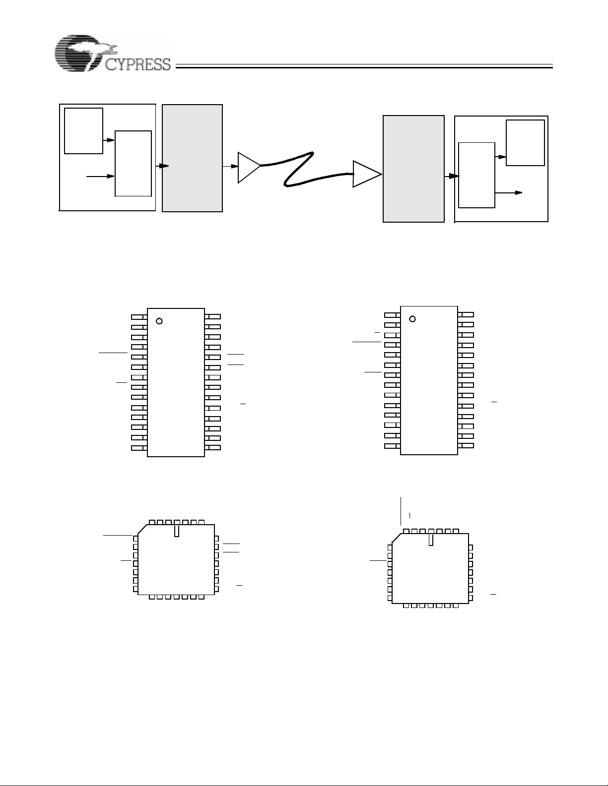
PROTOCOL
HOST
CY7B923
CY7B933
LOGIC
PROTOCOL
BUFFER
MESSAGE
TRANSMIT
7B923
TRANSMITTER
7B933
RECEIVER
BUFFER
RECEIVE
MESSAGE
SERIAL LINK
B923–3
HOST
Figure 1. HOTLink System Connections
CY7B923 Transmitter Pin Configurations
SOIC
Top View
j
7
6
5
4
RP
1
−
2
−
3
4
5
6
7
8
9
)
10
11
12
13
14
PLCC/LCC
Top View
CCN
V
OUTC+
43 12
5
6
7
8
9
10
11
1213 1514
6
5D4D3D2D1D0
D
OUTB
OUTC
OUTC+
V
CCN
BISTEN
GND
MODE
RP
V
CCQ
SVS(D
(Dh)D
(Dg)D
(Df)D
(Di)D
BISTEN
GND
MODE
V
CCQ
SVS(Dj)
(D
h)D7
7B923
−
OUTC−OUTB+
OUTB
7B923
28
27
26
25
24
23
22
21
20
19
18
17
16
15
−
OUTA+
OUTA
2726
28
25
FOTO
24
c
(D )b(D )
ENN
23
ENA
22
V
21
CKW
20
GND
19
SC/D
D
16
1718
d
(D )e(D )i(D )f(D )g(D )
OUTB+
OUTA+
OUTA
−
FOTO
ENN
ENA
V
CCQ
CKW
GND
SC/D(Da)
D
)
0(Db
)
D
1(Dc
)
D
2(Dd
)
D
3(De
B923–5
CCQ
(Da)
B923–4
CY7B933 Receiver Pin Configurations
2
Page 3
Maximum Ratings
CY7B923
CY7B933
(Abov e which the use ful lif e ma y be impai red. F or use r guidelines, not tested.)
Storage Temperature......................................−65°C to +150°C
Ambient Temperature with
Po wer Applied..................................................−55°C to +125°C
Supply Voltage to Ground Potential................. −0.5V to +7.0V
DC Input Voltage................................................ −0.5V to +7.0V
Output Current into TTL Outputs (LOW)......................30 mA
Output Current into PECL outputs (HIGH)...................−50 mA
Static Discharge Voltage ...........................................>4001V
(per MIL−STD−88 3, Method 3015)
Latch-Up Current.....................................................>200 mA
Operating Range
Ambient
Range
Commercial 0°C to +70°C 5V ± 10%
Industrial
Military
Temperature
−40°
C to +85°C 5V ± 10%
−55°
C to +125°C
V
CC
5V ± 10%
Case Temperature
Pin Descriptions
CY7B923 HOTLi nk Transmitter
Name I/O Description
D
0−7
(D
b − h
SC/D (Da) TTL In Special Cha ract er/Dat a Sele ct. A HIGH on SC/D whe n CKW ris es caus es the t r ansmit ter t o encode
SVS
(D
)
j
ENA TTL In Enable Parallel Data. If ENA is LOW on the rising edge of CKW, the dat a is loaded, encoded, and
ENN TTL In Enable Next Parallel Data. If ENN is LOW, the data appearing on D
CKW TTL In Clock Write . CKW is both t he clock frequency reference for the multiplying PLL that generates the
FOTO TTL In Fiber Optic Transmitter Off. FOTO determines the function of two of the three PECL transmitt er
TTL In Par allel Data Input. Data is cloc ked into the Transmitter on the rising edge of CKW if ENA is LOW
)
(or on the next rising CKW with ENN
sent. When MODE is HIGH, D
the patt ern on D
using the 8B/10B data alphabe t. When MODE is HIGH, SC/ D
same timing as D
as a control code (Spe cial Charac ter), while a LO W causes the data to be co ded
0−7
.
0−7
LOW). If ENA and ENN are HIGH, a Null character (K28.5) i s
0, 1, ...7
become D
b, c,...h
respectively.
(Da) acts as Da input. SC/D has the
TTL In Send Violation Symbol . If SVS is HIGH when CKW rises, a Vio lat ion symbol is encoded and sent
while the dat a on the parallel input s is ignored. If SVS is LOW , the state of D
and SC/D determines
0−7
the code sent. In normal or test mode, this pin ove rrides the BIST generator and forces the transmission of a Violation code. When MODE is HIGH (placing the transmitter in unencoded mode),
SVS (D
sent. If ENA
character (K 28.5) to f i ll the s pace between user da ta. ENA
it may be pulsed with each data byte to be sent . If ENA
) acts as the Dj input. SVS has the same timing as D
j
0−7
.
and ENN are HIGH, the data input s are ignored and the Transmitter will insert a Null
may be held HI GH/LO W c ont inuous ly or
is being used fo r data control, ENN will
normally be stra pped HIGH, but can be used for BIST function control.
at the next rising edge of
CKW is loaded, encode d, and sent. If ENA
and ENN are HIGH, the data appearing on D
0−7
next ri sing edg e of CKW will b e ignored and the Transmitter wi ll insert a Null cha racter to fi ll the space
between us er dat a. ENN
byte sent. If ENN
is being used for data control, ENA will normally be strapped HIGH, but can be
may be hel d HIGH/LOW continuously or it may be pulsed with each data
used for BIST function control.
high−speed transm it clock, and the byt e rat e writ e signal that synchronizes the parallel data input.
CKW must be connected to a crystal controlled time base that runs within the specified frequency
range of the Transmitter and Recei ver.
output pair s. If FOTO is LOW, the data encoded by the Transmitter wil l appear at the outputs continuously. If FOTO is HIGH, OUTA± and OUTB ± are forced to their “logic zero ” state (OUT+ = LOW
and OUT− = HIGH), causing a fiber optic transmit module to extinguish i ts light output. OUTC is
unaffected by the level on FOTO, and can be used as a loop-back signal source for board-level
diagnostic testing.
0−7
at the
3
Page 4
CY7B923
CY7B933
CY7B923 HOTLi nk Transmitter
(continued)
Name I/O Description
OUTA±
OUTB±
OUTC±
PECL Out Diffe renti al Seri al Dat a Ou tputs . T hese PECL 1 00K outp uts ( +5V r ef er enced) are capab le of dri ving
terminated trans mission lines or commercial fibe r optic tra nsmitter modules. Unused pairs of outputs
can be wire d to V
level on FOT O , and will remain at their “logical zero” states when FOTO is asserted. OUTC± is unaffected
to re duce po wer i f the ou tput is not r equ ired . OU TA± and OUTB± are contro lled by the
CC
by the l ev el on F OT O . (OUTA+ and OUTB+ are us ed a s a diff ere ntia l te st c loc k inp ut w hile in Test m ode, i. e.,
MODE=UNC ONNE CTED or f o rce d to V
CC
/2.)
MODE 3-Lev el I n Encoder Mode Select. The leve l on MODE determines the encoding method to be used. When
wired to GND, MODE selects 8B/10B encodi ng. When wired to V
and the bit pattern on D
V
/2) the internal bit-clock generator is disabled and OUTA+/OUTB+ become the differential bit clock to be
CC
used for factory test. In typical applications MODE is wired to V
goes directly to the shifter. When left floating (internal resistors hold the input at
a-j
CC
, data inputs bypass the encoder
CC
or GND.
BISTEN TTL In Built-In Sel f-Test Enable. When B ISTEN is LO W and ENA and ENN are HIGH, the transmitter sends an
altern ati n g 1−0 pattern (D10.2 or D21.5). When either ENA
or ENN is se t LO W a nd BIST EN is LO W , th e
transmitter begins a repeating test sequence that allows the T ransmitter and Receiver to work together to test
the function of the entire link. In normal use this input is held HIGH or wired to V
a free-running pattern generator that need not be initialized, but if required, the BIST sequence can be
initialized by momentarily asserting SVS while BISTEN
is LOW. BISTEN has the same timing as D
. The BIST generator is
CC
0−7
.
RP TTL Out Read Pulse. RP i s a 60% LO W d uty -c ycl e byt e -r ate pu lse t rai n sui t abl e f or the rea d pu l se i n C Y7C 42X
V
V
CCN
CCQ
FIFOs. The frequency on RP
the CKW duty cycle. Pulse widths are set by logic internal to the transmitter. In BIST mode, RP
HIGH for all but the last byte of a test loop. RP
Po wer for output driv ers.
Power for internal circuitry.
is the same as CKW when enabled by ENA, and duty cy cl e is in de pe nden t o f
will remain
will pulse LOW one byte time per BIST loop.
GND Ground.
CY7B933 HOTLi nk Receiver
Name I/O Description
Q
(Q
0−7
b − h
)
TTL Out Q
Parallel Data Output. Q
0−7
nously with CKR. When MODE is HIGH, Q
conta in t he m o st r ec ent l y re ce iv e d d ata. T he se ou tp uts ch an ge sync hr o -
0−7
0, 1, ...7
become Q
b, c,...h
respectively.
SC/D (Qa) TTL Out Special Character/Data Select. SC/D indicates the context of received data. HIGH indicates a Control
(Special Character) code, LOW indicates a Data character. When MODE is HIGH (placing the receiver in
Unencoded mode), SC/D
acts as the Qa output. SC/D has the same timing as Q
0−7
.
RVS (Qj) TTL Out Received Viol ation Symbol. A HIGH on RVS indicates that a code rule violatio n has been detected
in the received data stream. A LOW shows that no error has been detected. In BIST mode , a LOW
on RVS indicates correct operati on of the Transmitter, Receiver, and li nk on a byte-by-byte basis.
When MODE is HIGH (placing the recei ver in Unencoded m ode), R VS acts as the Q
the sam e ti ming as Q
0−7
.
output. RVS has
j
RDY TTL Out Data Output Ready. A LOW pulse on RDY indicates that new data has been received and is ready to be
delivered. A missing pulse on RDY
the transmitter as a pad between data inputs). In BIST mode RDY
shows that the received data is the Null character (normally inserted by
will remain LOW for all but the last byte
of a test loop and will pulse HIGH one byte time per BIST loop.
CKR TTL Out Clock Read. This byte rate clock output is phas e and frequency aligned to the incoming serial data
stream. RDY
, Q
, SC/D, an d R V S al l switch synchr on ou sly wit h t he ri si ng edge of thi s out pu t.
0−7
A/B PECL in Serial Data Input Select. This PECL 100K (+5V referenced) in put selects INA or INB as the active
data input. If A/B
A/B
is LOW INB is selected.
is HIGH, INA is connected to the shifter and signals connected to INA will be decoded. If
INA± Diff In Serial Data Input A. The dif ferential signal at the receiver end of the communication li nk m ay be
connected to the differential input pairs INA± or INB±. Either the I NA pair or the INB pa ir ca n be use d as
the main data input and the other can be used as a loopback channel or as an alternative data input selected
by the s t ate o f A/B
.
4
Page 5
CY7B923
CY7B933
CY7B933 HOTLi nk Receiver
(continued)
Name I/O Description
INB
(INB+)
PECL in
(Diff In)
Serial Data Input B. This pin is either a single-ended PECL data rec eiver (INB) or half of the INB
differenti al pair. If SO is wired to V
, then INB± can be used as differential line receiver interchangeably
CC
with INA±. If SO i s no rmal ly co nnec t ed an d l oa ded, IN B be co mes a s ing le- e nd ed PE CL 10 0K (+ 5V re f er enced) serial data input. INB is used as the test clock while in Test mode.
SI
(INB−)
PECL in
(Diff In)
Status Input. This pin is either a single-ended PECL status monitor input (SI) or half of the INB
differenti al pair. If SO is wired to V
with INA±. If SO is normally c onnected and loaded , SI becom es a sing le-ended PECL 100K (+ 5V refer enced)
, then INB± can be used as differential line receiver interchangeably
CC
status monitor input, which is translated into a TTL-level signal at the SO pin.
SO TTL Out Status Out. SO is the TTL-tran slated output of SI. It is typi cally used to trans late th e Carrier Detect
output from a fiber-optic receiver c onnected to SI. W hen this pin is normally connected and loaded
(without any e xternal pull-up resistor), SO will assume the same logic al level as SI and INB wil l
become a single-ende d PECL serial data inpu t. If the status m onit or tr anslat ion is not desi red, th en
SO may be wired to V
and the INB± pair may be used as a differential serial data input.
CC
RF TTL In Refram e Enab l e. RF c ontrols th e F r amer l ogic i n the Rec eiv er . When RF is held HIGH, each SYNC
(K28.5) symbol de tected in the shifter will fr ame the data th at follows . If is HIG H for 2,048 consecutiv e
bytes, th e internal f ra mer swi tches to do uble -b yte mode . When RF is held LO W, the reframing logic
is disabled. The incoming data stream is then conti nuously deserialized and decoded using byt e
boundaries set by the internal byte counter. Bit errors in the data stre am will not cause alias SYNC
characters to reframe the data erroneous ly.
REFCLK TTL In Referenc e Clock. REFCLK is the clock frequency reference for the clock/data synchroni zing PLL.
REFCLK sets the appro ximate c enter fre quency f or the int ernal PLL to tra ck the i ncoming bit stream.
REFCLK must be connected to a crystal-cont rolled time base t hat runs within the frequenc y limits of
the Tx/Rx pair , and the frequency must be the same as the transmitter CKW frequency (within
CKW±0.1%).
MODE 3-Level In Decoder Mode Select. The level on the M ODE pin determines the decoding method to be used.
When wired to GND, MODE selects 8B/10B decoding. When wired t o V
bypass the decoder and are sent to Q
V
/2) the internal bit clock ge nerator is disab led and INB b ecomes th e bit rat e test clo ck to be use d for f actory
CC
test. In typical applications, MODE is wired to V
directly . When left floating (internal resistors hold the MODE pin at
a−j
or GND.
CC
, registered shifter contents
CC
BISTEN TTL In Built-In Self-Test Enable. When BIST EN is LOW the Receiver awaits a D0.0 (sent once per BIST loop)
charact er and beg ins a conti nuou s te st seq uenc e that test s th e func tion alit y of t he Trans mitte r , the R ecei v er ,
V
V
CCN
CCQ
and the link connecting them. In BIST mode the status of the test can be monitored with RDY
outputs . In norma l us e B ISTE N
Power for output driv ers.
Power for internal circuitry.
is held HIGH or wired to VCC. BISTEN has the same timing as Q
and R V S
.
0−7
GND Ground.
CY7B923 HOTLink Transmitter Block Diagram
Description
Input Register
The Input regi ster holds t he data t o be proce ssed by the HO TLink tr ansmitt er a nd allo ws the i nput t iming to be made c onsistent with standar d FIFOs. The Input r egister is cloc ked by CKW
and loaded with information on the D
Two enable in pu ts (E NA
and ENN) al lo w the use r to ch oose when
data is loaded in the register. Asserting ENA
causes the inputs to be loaded in the register on the rising edge of
CKW. If ENN
(Enable Next, active LOW) is asserted when CKW
rises , the dat a present on the inpu ts on the n ext rising ed ge of CKW
will be loaded in to the In put r egister. If neither EN A
asserted LOW on the rising edge of CKW, then a SYNC (K28.5)
character is sent. These two inputs allow proper timing and function
for compatibility with either asynchronous FIFOs or clocked FIFOs
withou t ex t ernal lo gi c, as sho wn i n
Figure 5.
, SC/D, and SVS pins.
0−7
(Enable, active LOW)
nor ENN are
In BIST mode, the Input register becomes the signature pattern generator by logical ly con verting t he parall el Input register
into a Linear Fe edbac k Shift Reg is ter (LFSR). Whe n enab led ,
this LFSR will generat e a 511-byte sequence that includes all
Data and Special Ch aract er codes , incl uding t he e xpli cit viola tion symbols. This pattern provides a predictable but pseudo-random sequence that can be matched to an identical
LFSR in the Receiver.
Encoder
The Encoder transforms the input data held by the Input register into a form more suitable for transmission on a serial interface l ink. The co de used is spec ified b y ANSI X3.230 (F ibre
Channel) and t he IBM ESCON cha nnel ( cod e tab les are at t he
end of this datasheet). The eight D
data inputs are converted
0−7
to eit her a Data sym bol o r a Speci al Ch ar acter , dep endin g up on th e
state of the SC/D
input. If SC/D is HIGH, the data inputs represent
a control code and are encoded using the Special Character code
5
Page 6

CY7B923
CY7B933
table. If SC/D
code table. If a byte time passes with the inputs disabled, the Encoder will output a Special Character Comma K28.5 (or SYNC) that
will maintain link synchroniz ation. SVS input forces the transm ission of a spec i fi ed Viol at ion sy mb ol t o a ll o w th e us er t o check error
handling system logic in the controller or for proprietary applications.
The 8B/10B coding function of the Encoder can be bypassed
for systems that include an external coder or scrambler function as part of the cont roller. This bypass is controlled by setting the MODE select pin HIGH. When in bypass mode, D
(note that bit order is specified in the Fib re Channel 8B/10B co de)
become the ten inputs to the Shifter, with D
shifted out.
Shifter
The Shifter accepts parall el data from the Encoder once each
byte time and shi fts it to the serial inter face output buffers using
a PLL multiplied bit clock that runs at ten (10) times the byte
clock rate. Timing for the parallel transfer is controlled by the
counter included in the Clock Gene ra tor and is not af fe cte d by
signal le vels or timing at the i nput pins.
OutA, OutB, OutC
The serial interf ace PECL output buf fers (ECL10 0K reference d
to +5V) are the drivers for the serial media. They are all connected to the Shi fter and contain the same serial data. Two of
the output pairs (OUTA± and OUTB±) a re controlla ble by the
FOTO input and can be disabled by the system controller to force a
logical zero (i.e., “light off”) at the outputs. The third output pair
(OUTC±) is not affected by FOT O and will supply a continuous data
stream suitable for loop-back testing of the subsystem.
OUTA± and OUTB± will respond to FOTO input changes within a
few bit times. However, since FOTO is not synchronized with the
transmitter data strea m, the o utputs will be forced off or tur n ed on
at arbitrary points in a transmitted byte. This function is intended to
augmen t an extern al laser sa fety con troller an d as an aid f or Receiver PLL testing.
In wire-based systems, control of the outputs may not be required, and FOTO can be strapped LOW. The three outputs
are intended to add system and architectural flexibility by offering identical serial bit streams with separate interfaces for
redundant c onnec tions o r f or mu lti ple d est inati ons. Unneede d
outputs can be wired to VCC to disable and power do wn the un used output circuitry .
Clock Genera tor
The clock gener ator is an embed ded phase-l ock ed loop (PLL)
that takes a byte-rate reference clock (CKW) and multiplies it
by ten (10) to create a b it rate cl ock f or driving t he serial shif ter .
The byte rate reference comes from CKW, the rising edge of
which clocks data i nto the Input register . This cl ock must be a
crystal refe renc ed pulse stream that has a fre quenc y betwee n
the minimum and maximum specified for the HOTLink Transmitter/Receiver pair. Signals controlled by this block form the
bit cloc k and the t iming s ignal s th at control in ternal data t ransfers between the Input register and the Shifter.
The read pulse (RP
the PLL mu ltiplier. It is a byte-ra te pulse stre am with th e proper
phase and pulse widths to allow transfer of data from an asynchronous FIFO. Pulse width is independent of CKW duty cycle, since
proper ph ase a nd duty cy cle is ma intain ed by the P LL. Th e RP
is LO W , the data i nput s are con ve rted usi ng th e Dat a
a−j
being the first bit to be
a
) is deri ved f rom the fe edbac k coun ter us ed in
pulse stream will insure co rrect data transfers between asynchronous FIFOs and the transmitter input latch with no external logic.
Test Logic
Test logic includes the initialization and control for the Built-In
Self-Test (BIST) generat or , the mu lti ple x er for Tes t mode cloc k
distributio n, and control logi c to properly select the dat a encoding. Test logic is discussed in more detail in the CY7B923
HOTLink Transmitter Operating Mode Description.
CY7B933 HOTLink Receiver Block Diagram
Description
Serial Data Inputs
Two pairs of differential line receivers are the inputs for the
serial data stream. INA± or INB± can be selected with the A/B
input. INA± is selected with A/B HIGH and I NB± is selected with A/B
LOW. The threshold of A/B is compatib le wit h the ECL 10 0K sig nals
from PECL fiber optic interface modules. TTL logic elements can be
used to select the A or B inputs by adding a resistor pull-up to the
TTL driver connected to A/B
INB± will accommodate wire intercon nect with filtering losses or
transmission line attenuation greater than 20 db (V
can be directly connected to fiber optic interface modules (any ECL
logic f amily, not li mited to ECL 100K) . The commo n mode tole ranc e
will accommodate a wide range of signal termination voltages. The
highest HIGH input that can be tolerated is V
est LOW input that can be interpreted correctly is V
PECL-TTL Translator
The function of the INB(INB+) input and the SI(INB−) input is
defined by the connections on the SO output pin. If the
PECL/TTL transl ator function is not requi red, the SO output is
wi red to V CC. A sensor circuit will detect th is connection and
cause the inputs to become INB± (a differential line-receiver seri-
al-data input). If the PECL/TTL translator function is required, the
SO output i s connected to its normal TTL load (typi cally one or mo re
TTL inpu ts, but no pull- up resi stor) and the I NB+ i nput bec omes I NB
(single-ended ECL 100K, serial data input) and the INB− input becomes SI (si ngl e -en de d, EC L 10 0K st at us inp ut) .
This positiv e-ref erenced PECL-to-TTL tr anslator i s provi ded to
eliminate external logic between an PECL fiber-optic interface
module “carrie r detect” output and the TTL input in the control
logic. The input threshold is com patible with ECL 100K lev els
(+5V refer enc ed). I t can also be use d as part of the l ink st at us
indication logi c for wire connect ed systems.
Clock Synchronization
The Clock Synchronization function is performed by an embedded phase-locked loop (PLL) that tracks the frequency of
the incoming bi t stream and aligns the phase of its internal bit
rate cloc k to the serial data tr ansition s. This b lock cont ains the
logic to transf er the data from the Shif ter to the Decode registe r
once every byte. The counter that controls this transfer is initialized by the Frame r l ogic. CKR is a buffered output derived
from the bit counter used to control the Decode register and
the output register transfers.
Clock output logic is designed so that when reframing causes
the counter sequence to be interrupted, the period and pulse
width of CKR will never be less than normal. Reframing may
stretch the perio d of CKR b y up to 90% , and e ither CKR Pulse
Width HIGH or Pulse Width LO W may be stret ched, depending
on when reframe occurs.
. The di f f e rent ia l th re sho l d of I NA± and
> 50 mv) or
DIF
= VCC, and the low-
IN
= GND+2.0V.
IN
6
Page 7

CY7B923
CY7B933
The REFCLK input provides a byte-rate reference frequency
to improve PLL acquisition time and limit unlocked frequency
excursions of the CKR when no data is present at the serial
inputs. The frequency of REFCLK is required to be within
±0.1% of the frequency of the clock that drives the transmitter
CKW pin.
Framer
Framer logic checks the incoming bit stream for the pattern
that defi nes the b yte boundari es. Thi s combinatori al logic f ilter
looks for the X3.230 symbol defined as a Special Character
Comma (K28.5). When it i s found, the free-runnin g bit counter
in the Clock Synchronization block is synchronously reset to
its initial state, thus framing the data correctly on the correct
byte boundaries.
Random errors that occur in the serial data can corrupt some
data patterns into a bit pattern identical to a K28.5, and thus
cause an erroneous d ata-fr aming erro r. The RF input pr eve nts
this b y inhibi ting r eframing during t imes when n ormal messag e
data is pres ent. When RF is held LOW, the HOTLin k receiver
will deserializ e the incoming data with out trying to ref rame th e
data to i ncoming pat terns. When RF rises , R DY
until a K28 .5 ha s been d etecte d, aft er wh ich RDY
normal function. While RF is HIGH, it is possible that an error could
cause misframing, after which all data will be corrupted. Likewise,
a K28.7 fol lowed by D11 .x, D2 0.x, or an SV S (C0. 7) followed by
D11.x will create alias K28.5 characters and cause erroneous framing. These sequences must be avoided while RF is HIGH.
If RF remains HIGH for greater than 2048 bytes, the framer
converts to double-byte framing, requiring two K28.5 characters aligned on the same b yte boundary wi thin 5 b ytes in or der
to reframe . Double-byt e framing greatl y reduces the possi bility
of erroneousl y ref raming to an aliased K28.5 character.
Shifter
The Shifter accepts serial inputs from the Serial Data inputs
one bit at a tim e, as c locked by the Clock Synchroniza tion l ogic. Data is transferred to the Framer on each bit, and to the
Decode register once per byte.
Decode Register
The Decode register accepts data from the Shifter once per
byte as determined by the logic in the Clock Synchronization
block. It is presented to the Decoder and held until it is transferred to the output latch.
will be inhibited
will resume its
Decoder
Parallel data is transformed from ANSI-specified X3.230
8B/10B codes back to “raw data” in the Decoder. This block
uses the standard decoder patterns shown in the Valid Data
Characters and Vali d Special Charact er Codes and Sequences sections of this dat ash eet. Data patte rns are signaled b y a
LOW on the SC/D
naled by a HIGH on the SC/D
errors are signaled as errors by a HIGH on the RVS output and by
specific Special Character codes.
Output Register
The Output regist er hol ds the re co vere d data (Q
RVS) and aligns it with the recovered byte clock (CKR). This synchronization insures proper timing to match a FIFO interface or other logic that requires glitch free and specified output behavior. Outputs cha ng e syn ch ron ou sly wit h th e ri si ng ed ge of CKR .
In BIST mode, this register becomes the signature pattern
generator and checker by logically converting itself into a Linear Feedback Shi ft Regist er (LFSR) pattern generat or. When
enabled, this LFSR will generate a 511-byte sequence that
includes all Data and Special Character codes, including the
explici t violat ion sym bols . This pa ttern pro vides a predic tabl e
but pseudo-r andom sequen ce that can be mat ched to an iden tical LFSR in the Transmitter. When synchronized, it checks
each byte in the Decoder with each byte generated by the
LFSR and shows errors at RVS. Patterns generated by the
LFSR are compared after being buf fered to the outp ut pins and
then fed back to the comparators, allowing test of the entire
receive func ti on.
In BIST mode, th e LFSR is i niti aliz ed b y th e fir st occur rence o f
the transmitter BIST loop start code D0.0 (D0.0 is sent only
once per BIST loop). Once the BIST loop has been started,
RVS will be HIGH for pattern mismatches between the received sequence and the internally generated sequence.
Code rule violations or running disparity errors that occur as
part of the BIST loop will not cause an error indication. RDY
will pulse HIGH once per BIST loop and can be used to check test
pattern pr ogr e ss . The re cei ver BIST gen er at or ca n be rein it i ali ze d
by leaving and re-entering BIST mode.
Test Logic
Test logic includes the initialization and control for the Built-In
Self-Test (BIST) generat or , the mu lti ple x er for Tes t mode cloc k
distribut ion, and control logic for the decoder. Test logic is discussed in more detail in the CY7B933 HOTLink Recei ver Operating Mode Description
output an d S peci a l Cha r act e r pat te rns are s i g-
output. Unused patterns or disparity
, SC/D, and
0−7
7
Page 8
CY7B923
CY7B933
CY7B923/CY7B933 Electrical Characteristics
Over the Operating Range
[1]
Parameter Description Te st Conditions Min. Max. Unit
TTL OUTs, CY7B923: RP; CY7B933: Q
V
OHT
V
OLT
I
OST
TTL INs, CY7B923: D
V
IHT
V
IL T
I
IHT
I
IL T
Output HIGH Voltage IOH = − 2 mA 2.4 V
Output LOW Voltage IOL = 4 mA 0.45 V
Output Short Circuit Current V
, SC/D, SVS, ENA, ENN, CKW, FOTO, BISTEN; CY7B933: RF, REFCLK, BISTEN
0−7
Input HIGH Voltage Com’l, Ind’l, & Mil 2.0 V
Input LOW Voltage
Input HIGH Current VIN = V
Input LOW Current VIN = 0.0V
Transmitter PECL-Compatible Output Pins: OUTA+, OUT A−, OUTB+, OUTB−, OUTC+, OUTC
V
V
V
OHE
OLE
ODIF
Output HIGH Voltage
(V
referenced)
CC
Output LOW Voltage
(V
referenced)
CC
Output Differential Voltage
|(OUT+) − (OUT−)|
, SC/D, RVS, RD Y, CKR, SO
0−7
OUT
=0V
[2]
Ind’l & Mil
(CKW and FOTO , only)
−15 −90
2.2 V
−0. 5
CC
−10
−
Load = 50Ω to
V
− 2V
CC
Load = 50Ω to
V
− 2V
CC
Com’l V
Ind’l & Mil V
Com’l V
Ind’l & Mil V
CC
CC
CC
CC
−1.03
−1.05
−1.86
−1.96
V
V
V
V
Load = 50 ohms to VCC − 2V 0.6 V
CC
CC
0.8 V
+10
− 500 µA
−0.83
CC
−0.83
CC
−1.62
CC
−1.62
CC
Receiver PECL-Compatibl e Input Pins: A/B, SI, INB
V
V
I
I
IHE
ILE
IHE
ILE
[3]
[3]
Input HIGH Voltage Com’l V
Input LOW Voltage Com’l 2.0 V
Input HIGH Current VIN = V
Input LOW Current VIN = V
Max. +500
IHE
Min. +0.5
ILE
Differential Li ne Receiver Input Pins: INA+, INA−, INB+, INB
V
DIFF
Input Differential Voltage
Ind’l & Mil V
Ind’l & Mil 2.0 V
−
CC
CC
−1.165
−1.14
V
V
CC
CC
CC
CC
−1.475
−1.50
50 mV
|(IN+) − (IN−)|
V
V
I
I
IHH
ILL
IHH
ILL
[4]
Highest Input HIGH Voltage V
CC
Lowest Input LOW Voltage 2.0 V
Input HIGH Current VIN = V
Input LOW Current VIN = V
Max. 750
IHH
ILL
Min.
−200 µA
Miscellaneous Typ. Max.
[5]
I
CCT
[6]
I
CCR
Notes:
1. See the last page of this specification for Group A subgroup testing information.
2. Tested one output at a time, output shorted for less than one second, less than 10% duty cycle.
3. Applies to A/B
4. Input currents are always positive at all voltages above VCC/2.
5. Maximum I
V
CC
into V
current to V
6. Maximum I
outputs unloaded. I
the load currents f o r each output pin. T he total b uff er quies cent curr ent is 10m A max ., and max. T TL load c urrent f or eac h output pin can be calculated as fol lows: Where
R
L
process corner and temperature condition.
T ransmitter Power Supply
Current
Receiver Power Supply
Current
only .
is measured with VCC = Max., one PECL output pair loaded with 50 ohms to V
CCT
= 5.0V, TA = 25°C, one output pai r loaded with 50 ohms to VCC − 2.0V , others tied to VCC, BISTEN = LOW. I
is determined by PECL load cur rents , typically 30 mA with 5 0 ohms to VCC − 2.0V. Each additional enabled PECL pair adds 5 mA to I
CCN
as described. When calculating the contribution of PECL load currents to chip power dissipation, the output load current should be multiplied by 1V instead of VCC.
CCN
is measured with VCC = Max., RF = LO W, and outputs un loaded. Typical I
CCR
=equivalent load resistance, CL=capacitive load, and F
includes current into V
CCR
(pins 21 and 24). Curre nt into V
CCQ
I
I CCN
TTLPin
Freq. = Max. Com’l 65 85 mA
Ind’l & Mil 75 95 mA
Freq. = Max. Com’l 120 155 mA
Ind’l & Mil 135 160 mA
− 2.0V , and other PECL outputs ti ed to VCC. T y pical I
+
CC
is measured with VCC = 5.0V, TA = 25°C, RF = L O W, BISTEN = LOW, and
CCR
(pin 9) is determined by the total TTL output buff er quiescent cur rent plus the sum of all
CCN
0.95) (
*5)*0.3
V
CCN
R
L
=frequency in MHz of data on pin. A derating factor of 1.1 has been included to account for worst
pin
V
CCN
)
*
2
)1.5 *
C
L
includes current into V
CCT
*1.1
F
pin
is measured with
CCT
(pin 9 and pin 22) only. Current
CCQ
and an additional load
CCT
mA
V
V
µA
V
V
V
V
V
V
V
V
µA
µA
V
µA
8
Page 9
CY7B923
CY7B933
Capacitance
[7]
Parameter Description Tes t Condi tions Max. Unit
C
IN
Input Capacit ance TA = 25°C, f0 = 1 MHz, VCC = 5.0V 10 pF
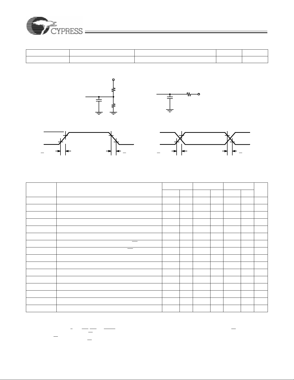
AC Test Loads and Waveforms
5V
OUTPUT
R1=910
R2=510
C
(Includes fixture and
probe capacitance)
<30pF
L
Ω
Ω
C
L
(a) TTL AC Test Load (b) PECL AC Test Load
3.0V
GND
<1ns <1ns
1.0V
3.0V
2.0V
(c) TTL Input Test Waveform (d) PECL Input Test Waveform
Transmitter Switch ing C h aracteri sti cs
R1
R2
2.0V
1.0V
B923–9
Over the Operating Range
2
V
−
CC
C
L
V
IHE
V
20%
ILE
<1ns <1ns
[1]
R
L
80%
[8][8]
V
IHE
V
ILE
=50
R
Ω
L
C
<5pF
L
(Includes fixture and
probe capacitance)
80%
B923–8
20%
B923–10
7B923-155 7B923 7B923-400
Parameter Description
t
CKW
t
B
t
CPWH
t
CPWL
t
SD
t
HD
t
SENP
t
HENP
t
PDR
t
PPWH
t
PDF
t
RISE
t
FALL
t
DJ
t
RJ
t
RJ
Notes:
7. Tested initially and after any design or process changes that may affect these parameters, but not 100% tested.
8. Cypress uses constant current (ATE) load configurations and forcing functions. This figure is for reference only.
9. Transmitter t
10. Data includes D
11. t
12. Loading on RP
13. While sending continuous K28.5s, RP unloaded, ou tputs loaded to 5 0Ω to V
14. While sending continuous K28.7s, after 100,000 samples measured at the cross point of differential outputs, time referenced to CKW input, over the operating
SENP
range.
and t
Write Clock Cycle 62.5 66.7 30.3 62.5 25 62.5 ns
Bit Time
[9]
6.25 6.67 3.03 6.25 2.5 6.25 ns
CKW Pulse Width HIGH 6.5 6.5 6.5 ns
CKW Pulse Width LOW 6.5 6.5 6.5 ns
Data Set-Up Time
Data Hold Time
Enable Set-Up Time (to insure correct RP)
Enable H o ld Tim e (t o in s u re co rr e ct RP)
Read Pulse Rise Alignment
Read Pulse HIGH
Read Pulse Fall Ali gnm ent
PECL Output Rise Time 20−8 0% (PECL Test Load)
PECL Output Fall Time 80−20% (PECL Test Load)
Deterministic Jitter (peak-peak)
Random Jitter (peak-peak)
Random Jitter (σ)
is calculated as t
B
, SC/D , SVS, ENA, EN N, and BISTEN. tSD and tHD minimum timing assu res corre ct data load on r ising edge of CKW, but not R P function or timing.
0−7
timing insures c orrect RP fun ction and cor rect data lo ad on t he rising edg e of CKW.
HENP
is the standard TT L te st load s ho wn in p art (a) of A C Test Loads and Wa v ef orms e xcept CL = 15 pF .
[10]
[10]
[12]
[12]
[12]
[7, 13]
[7, 14]
[7,14]
/10. The byt e rate is on e tent h of the bit rate.
CKW
[11]
[11]
[7]
[7]
2.0V, over the operating r ange.
−
CC
5 5 5 ns
0 0 0 ns
6tB + 8 6tB + 8 6tB + 8 ns
0 0 0 ns
−4
−3
4t
B
−3
6t
B
−4
2
−3
4t
B
−3
6t
B
−4
2
−3
4t
B
−3
6t
B
1.2 1.2 1.2 ns
1.2 1.2 1.2 ns
35 35 35 ps
175 175 175 ps
20 20 20 ps
UnitMin. Max Min. Max Min. Max
2 ns
ns
ns
9
Page 10

CY7B923
CY7B933
Receiver Switching Characteristics
Over the Operating Range
[1]
7B933-155 7B933 7B933-400
Parameter Description
t
CKR
t
B
t
CPRH
t
CPRL
t
RH
t
PRF
t
PRH
t
A
t
ROH
t
H
t
CKX
t
CPXH
t
CPXL
t
DS
t
SA
t
EFW
Notes:
15. The period of t
above.
16. Rec ei ver t
17. Data includes Q
18. tA, t
19. REFCLK has no phase or frequency relationship with CKR and only acts as a centering reference to reduce clock synchronization time. REFCLK must be
within 0.1% of the transmitter CKW frequency, necessitating a ±500-PPM crystal.
20. The PECL switching threshold is the midpoint between the PECL− V
21. Static alignment is a measure of the alignment of the Receiver sampling point to the center of a bit. Static alignment is measured by sliding one bit edge in
3,000 nominal transitions until a byte error occurs.
22. Error Free Window is a measure of the time window between bit centers where a transition may occur without causing a bit sampling error. EFW is measured
over the operating range, input jitter < 50% Dj.
Read Clock Peri od (No Serial Data Input), REFCLK
as Reference
Bit Time
[15]
[16]
Read Clock Pulse HIGH 5t
Read Clock Pulse LOW 5t
RDY Hold Time t
RDY Pulse Fall to CKR Rise 5t
RDY Pulse Width HIGH 4t
Data Access Time
Data Hold Time
Data Hold Time from CKR Rise
REFCLK Clock Period Referenced to CKW of
Transmitter
[17, 18]
[17, 18]
[17, 18]
[19]
REFCLK Clock Pulse HIGH 6.5 6.5 6.5 ns
REFCLK Clock Pulse LOW 6.5 6.5 6.5 ns
Propagation Delay SI to SO (note PECL and TTL
thresholds)
Static Alignment
Error Free Window
CKR
is calculated as t
B
0−7
, and tH specifications are only valid if all outputs (CKR, RDY, Q
ROH
[20]
[7, 21]
[7, 22]
will match the period of the transmitter CKW when the receiver is receiving serial data. When data is interrupted, CKR may drift to one of the range limits
/10 if no data is being rec eived, or t
CKR
, SC/D, and R VS.
/10 if data is be ing rece ived. See not e.
CKW
, SC/D , a nd R V S) are loa ded with s imilar DC and AC loads.
0−7
, and VOL specification (appr o ximately VCC − 1.35V). The T TL sw itch ing thres hold is 1.5V.
OH
−1
+1
6.25 6.67 3.03 6.25 2.5 6.25 ns
−3
B
−3
B
−2.5
B
−3
B
−3
B
−2
2t
t
B
2t
−0.1
B
−2.5
−3
B
2tB+42t
+0.1
20 20 20 ns
100 100 100 ps
0.9t
B
5t
5t
t
B
5t
4t
t
B
2t
−0.1
0.9t
−1
−3
B
−3
B
−2.5
−3
B
−3
B
−2
B
−2.5
−3
B
B
+1
t
2tB+4 2t
t
+0.1
−1
5t
B
5t
B
−2.5
B
5t
B
4t
B
B
−2.5
B
2t
B
−0.1
0.9t
−3
−3
−3
−3
−2
−3
B
2tB+4 ns
+0.1 %
UnitMin. Max Min. Max. Min . Max.
+1 %
ns
ns
ns
ns
ns
ns
ns
10
Page 11
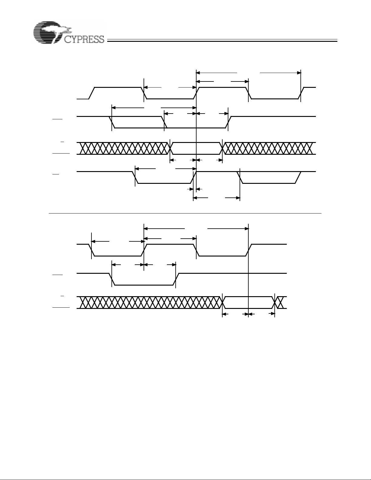
Switching Waveforms for the CY7B923 HOTLink Transmitter
t
t
PDF
CPWL
t
SD
VALID DATA
t
SD
t
PDR
t
HENP
t
HD
t
PPWH
CKW
ENA
D
0–D7
SC/D
,
SVS,
BISTEN
RP
t
SENP
NOTES
10,11
,
t
CPWH
t
CKW
CY7B923
CY7B933
DISABLED
ENABLED
B923–11
CKW
ENN
D
0–D7
SC/D
,
SVS,
BISTEN
t
CKW
t
t
CPWL
t
SD
CPWH
t
HD
,
VALID DATA
t
SD
t
HD
B923–12
11
Page 12

Switching Waveforms for the CY7B933 HOTLink Receiver
t
CKR
t
CPRH
CKR
t
CPRL
CY7B923
CY7B933
RDY
Q
Q
−
0
SC/D,RVS,
REFCLK
t
PRH
t
PRF
t
A
t
H
,
7
t
CPXL
SI
V
BB
t
CPXH
t
RH
t
CKX
t
ROH
B923–13
B923–14
SO
NOTE
StaticAlignment
tB/2−t
INA± ,
INB±
t
DS
20
SA
SAMPLE WINDOW
t
B
/2−t
1.5V
SA
B923–16
12
B923–15
Error-Free Window
INA
±
INB
±
BIT CENTER BIT CENTER
t
EFW
t
B
B923–17
Page 13

D0−7,
SC/D
SVS
CKW
ENA
,
RP
DATA
LATCHED IN
DATA
TRANSMITTER LATENCY = 21t
CY7B923
CY7B933
10ns
−
B
OUTX
±
K28.5
Figure 2. CY7B923 Transmitter Data Pipeline
HOTLink CY7B923 Transmitter and CY7B933
Recei ver Operation
The CY7B923 Transmitter operating with the CY7B933 Receiver form a general purpose data communications subsystem capable of transporting user data at up to 33Mbytes
per second (40 Mby tes per second for -400 de vices ) ov er several types of serial interface media.
of data through the HOTLink CY7B923 transmitter pipeline. Data is
latched into the transmitter on the rising edge of CKW when enabled
by ENA
or ENN . RP is asserted LOW with a 60% LOW/40% HIGH
duty cycle when ENA
is LOW. RP may be used as a read strobe for
accessing data stored in a FIFO. The parallel data flows through the
encoder and is then shifted out of the OUTx± PECL drivers. The
bit-rate clock is generated internally from a multiply-by-ten PLL clock
generator. The latency through the transmitter is approximately 21tB
− 10 ns over the operating range. A more complete description is
found in the section CY7B923 HOTLink T ransmitter Operating Mode
Description
Figure 3
.
illustrates the data flow through the HOTLink
CY7B933 receiver pipeline. Serial data is sampled by the re-
Figure 2
illustrates the flow
K28.5
DATA SENT
DATA
B923–18
ceiver on the INx± inputs. The receiver PLL locks onto the
serial bit stream and generates an internal bit rate clock. The
bit stream is deserial ized, decoded and the n presented at the
parallel output pins. A by te rate clock (bit clock ÷ 10) synchronous with the parallel data is presented at the CKR pin. The
RDY
pin will be asserted to L OW to indicate that dat a or cont rol
characters are present on the output s . RD Y
will not be asserted LOW in a field of K28.5s except f or any single K28.5 or the
last one in a cont in uous se ries of K28.5’s. The latency t hrough
the receiver is approximately 24t
range. A more complete description of the receiver is in the
+ 10 ns over the operating
B
section CY7B933 HOTLink Receiver Operating Mode Description
The HOTLi nk Receiver has a bui lt- in b yte fr ame r that synchro nizes the Re ceiv er pipel ine wi th i ncoming SYNC (K2 8.5) c haracters.
Figure 4
illustrates the HOTLink CY7B933 Receiver framing
operation. The Framer is enabled when the RF pin is asserted HIGH.
RF is latched into the receiver on the falling edge of CKR. The framer
looks for K28.5 characters embedded in the serial data stream. When
a K28.5 is found, the framer sets the parallel byte boundary for subsequent data to the K28.5 boundary . While the framer is enabled, the
RD Y
pin indicates the status of the framing operation.
SERIAL DATA IN
INX
±
CKR
Q0−7,
SC/D
,
RVS
RDY
RDY IS LOW FOR DATA
DATA
DATA
RECEIVER LATENCY= 24t
RDY
IS HIGH IN FIELD OF K28.5S
+10ns
B
K28.5
IS LOW FOR LAST K28.5
RDY
Figure 3. CY7B933 Receiver Data Pipeli ne in Encoded Mode
13
DATAK28.5
PARALLEL
DATA
B923–19
OUT
Page 14
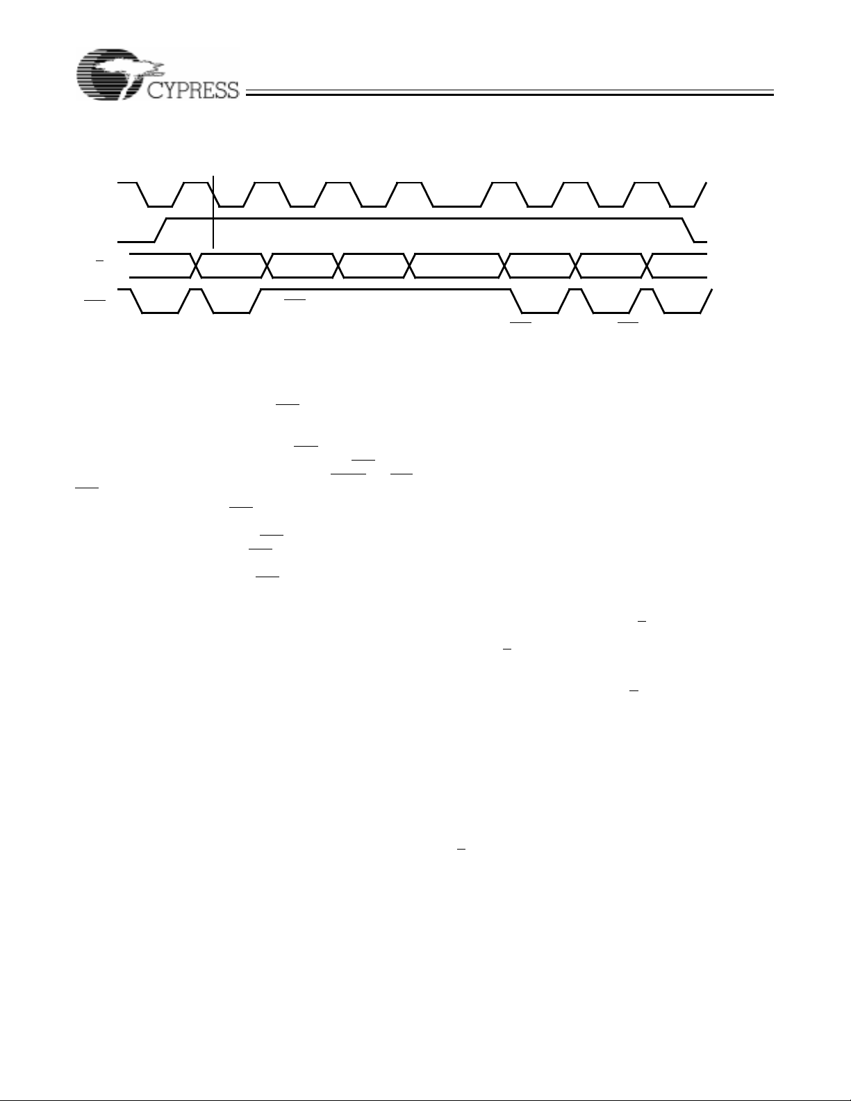
CY7B923
CY7B933
CKR
RF
Q0−7,
SC/D
RVS
RDY
RF LATCHED ON
FALLING EDGE OF CKR
,
RDY IS HIGH WHILE WAITING FOR K28.5
DATA BOUNDARY CHANGES
Figure 4. CY7B933 Framing Operation in Encoded Mode
When the RF pin is asserted HIGH, RDY
leaves it normal mode
of operation and is asserted HIGH while the framer searches the data
stream for a K28.5 character. After the framer has synchronized to a
K28.5 character, the Receiver will assert the RD Y
K28.5 character is present at the parallel output. The RDY
then resume its normal operation as dictated by the MODE
pin LOW when the
pin will
and BIS-
TEN pins.
The normal operation of the R DY
pin in encoded mode is to signal
when parallel data is present at the output pins by pulsing LOW with
a 60% LOW/40% HIGH duty cycle. RDY
field of K28.5 characters; however , RDY
does not pulse LOW in a
does pulse LOW for the l ast
K28.5 character in the field or for any single K28.5. In unencoded
mode, the normal operation of t he RDY
pin is to signal when any
K28.5 is at the parallel output pins.
The Transmitter and Receiver parallel interface timing and
functional ity can be made to ma tch the timing and functional ity
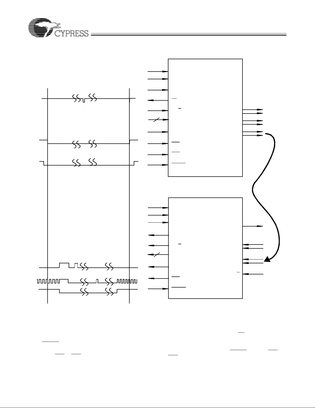
of either an asynchronous FIFO or a clocked FIFO by appropriately connecting signals (See
Figur e 5
). Proper operation of
the FIFO interface depends upon various FIFO-specific access and
response specifications.
The HOTLink Transmitter and Receiver serial interface provides a seamless interface to various types of media. A minimal number of external components are needed to properly
terminate transmission lines and provide PECL loads. For
proper power supply decoupling, a single 0.01 µF for each de-
vice is all that is required to bypass the VCC and GND pins.
6
illustrates a HOTLink T ransmitter and Receiver interface to fiber op-
Figure
tic and copper media. More informat ion on interfacing HOTLink to
various media can be found in the
HOTLink Design Considerations
application note.
CY7B923 HOTLink T ransmitter Operati ng Mode
Description
In normal operation, the Transmitter can operate in either of
two modes. The Encoded mode allows a user to send and
CKR STRETCHES AS
DATADATADATADATADATA DATA DATA
K28.5
RDY IS LOW
FOR K28.5
RDY RESUMES
NORMAL
OPERATION
B923–20
receive eight (8) bit data and control information without first
converting i t to transmission charact ers. The Byp ass mode is
used for systems in which the encoding and decoding is performed in an external protocol controller.
In either mode, data is loaded into the Input register of the
Transmitter on the rising edge of CKW. The input timing and
functional response of the Transmitter input can be made to
match the timing and functionality of either an asynchronous
FIFO or a clocked FIFO by an appropriate c onnection of input
signals (See
Figure 5
). Proper operation of the FIFO interface depends upon various FIFO-specific access and response specifications.
Encoded Mode Operation
In Encoded mode the input data is interpreted as eight bits of
data (D
input bit (SVS). If the context of the data is to be norm al messa ge
data, the SC/D
− D7), a context control bit (SC/D), and a system diagnostic
0
input should be LOW, and the data should be encoded using the valid data character set described in the Valid Data Characters section of this datasheet. If the context of the data is to be
control or protocol information, the SC/D
input will be HIGH, and the
data will be encoded using the valid special character set described
in the Valid Special Character Codes and Sequences section. Special characters include all protocol characters necessary to encode
packets for Fibre Channel, ESCON, proprietar y syst ems, and diagnostic purposes.
The diagnosti c charact ers and seq uences a va ilable as Special
Characters i nclude thos e for Fi bre Channel link testi ng, as well
as codes to b e used for testing system response to lin k errors
and timing. A Violation symbol can be explicitly sent as part
of a user data packet (i.e., send C0.7; D
SC/D
= 1), or it can be sent in response to an external system using
= 111 00000 and
7−0
the SVS input. This will allo w system diagnostic logic to ev al uate the
errors in an unambiguous manner, and will not require any modification to the transmission interface to force transmission errors for testing purposes.
14
Page 15

CY7B923
CY7B933
CLOCKED FIFOASYNCHRONOUS FIFO
FROM CONTROLLER
7C42X/3X/6X/7X
RQ
ENA D
7B923 7B923
HOTLINK TRANSMITTER
HOTLINK RECEIVER
7B933 7B933
7C44X/5X
0−8
9
,SC/DCKW RP ENN D
0−7
,SC/DCKR
0−7
9
ENR Q
CKR
HOTLINK TRANSMITTER
HOTLINK RECEIVER
RDY Q
0−7
0−7
0−8
9
,SC/DCKW
,SC/DCKRRDY Q
9
WD
7C42X/3X/6X/7X 7C44X/5X
0−8
Figure 5. Seamless FIFO Interface
Bypass Mode Operation
In Bypass mode the input data is interpreted as ten (10) bits
(D
), SC/D (Da), and SVS (Dj) of pre-encoded transmission data to
b-h
be serialized and sent over the link. This data can use any encoding
method suitable to the designer. The only restrictions upon the data
encoding method is t hat i t contai n suitable transition densit y for the
Receiver PLL data synchronizer (one per 10 bit byte), and that it be
compatible with the transmission media.
Data loaded into the Input register on the rising edge of CKW
will be loaded into the Shifter on the subsequent rising edges
of CKW. It will then be shifted to the outputs one bit at a time
using the i nternal cloc k gener ated b y the cloc k genera tor. The
first bit of the transmission character (Da) will appear at the output
(OUT A±, OUTB±, and OUTC±) after the next CKW edge.
While in either the Encoded mode or Bypass mode, if a CKW
edge arrives when the inputs are not enabled (ENA
and ENN
both HIGH), the Encoder will insert a pad character K28.5 (e.g., C5.0)
CKW
ENW D
CLOCKED FIFOASYNCHRONOUS FIFO
0−8
B923–21
to maintain proper link synchronization (in Bypass mode the proper
sense of running disparity cannot be guaranteed for the first pad character, but is correct for all pad characters that follow). This automatic
insertion of pad characters can be inhibited by insuring that the T ransmitter is always enabled (i.e., ENA
or ENN is hard-wired LOW).
PECL Output Functional and Connection Options
The three pairs of PECL outpu ts all cont ai n the same i nf ormation and are intended for use in systems wit h multiple c onnections. Each out put pair may be connected to a different serial
media, each of which may be a different length, link type, or
interf ace technology. For systems that do not requir e all three
output pairs, the unused pairs should be wired to V
mize the power dissipated by the output circuit, and to minimize un-
to mini-
CC
wanted noise generation. An internal voltage com parator detects
when an output differential pair is wired to V
source for that pair to be disabled. This results in a power savings of
, causing the current
CC
around 5 mA for each unused pair.
15
Page 16

CY7B923
CY7B933
In system s that require the outputs to be shut off during s om e
periods when link transmission is prohibited (e.g., for laser
safety f unctions), the FOTO input can be asserted. While i t is
possible to insure that the output state of the PECL drivers is
LOW (i.e., light is off) by sending all 0’s in Bypass mode, it is
often inconvenient to insert this level of control into the data
transmission channel, and it is impossible in Encoded mode.
FOT O is p ro vided to s impl ify and a ugment t his contro l fu nct ion
(typically found in laser-based transmission systems). FOTO
will force OUTA+ and OUTB+ to go LOW, OUTA− and OUTB−
to go HIGH, while al lowing OUTC ± to continue to function normally (OUTC is typically used as a diagnosti c feedback and cannot be
disabled). This separation of function allows various system configurations without undue load on the control function or data channel
logic .
Transmitter Serial Data Characteristics
The CY7B923 HOTLink Transmitter serial output conforms to
the requirements of the Fibre Channel specification. The se-
.01UF
922
CY7B923
Transmitter
(Da)
(Db)
(Dc)
(Dd)
(De)
(Di)
(Df)
(Dg)
(Dh)
(Dj)
CKW
REFCLK
(Qa)
(Qb)
(Qc)
(Qd)
(Qe)
(Qi)
(Qf)
(Qg)
(Qh)
(Qj)
CKR
4
VCC
OUTA+
OUTA–
OUTB+
OUTB–
OUTC+
OUTC–
GND
9 2421
VCC
CY7B933
Receiver
GND
20
86
20
6
IB+
IB–
IA+
IA–
27
26
Unused Output Left
28
Open to Minimize
1
Power Dissipation
2
1
Tx PECL Load
.01UF
3
2
28
27
Config
Control
Status
Data
Config
Control
Status
Data
7
MODE
25
FOTO
5
BISTEN
&
&
24
23
19
18
17
16
15
14
13
12
11
10
21
8
26
25
4
23
3
5
7
19
18
17
16
15
14
13
12
11
10
22
ENN
ENA
RP
SC/D
D0
D1
D2
D3
D4
D5
D6
D7
SVS
MODE
BISTEN
SO
A/B
RF
RDY
SC/D
D0
D1
D2
D3
D4
D5
D6
D7
RVS
rial data output is contr olled b y an internal Pha se-Loc ked Loop
that multiplies the frequency of CKW by ten (10) to maintain
the proper bit clock frequency. The jitter characteristics (including both PLL and logic components) are shown below:
Deter ministic Jitter (D
sured while sending a continuous K28.5 (C5.0).
Random Jitter (R
while sending a continuous K28.7 (C7.0).
) < 35 ps (peak-pea k). Typically mea-
j
) < 175 ps (peak-peak). Typically measured
j
Transmitter Te st Mode Description
The CY7B923 Transmitter offers two types of test mode operation, BIST m ode and Test mode. In a normal system application, the Built-In Self-Test (BIST) mode can be used to check
the functionality of the Transmitter, the Receiver, and the link
connecting them. This mode is available with minimal impact
on user system logic, and can be used as part of the normal
system diagnosti cs. Typical connect ions and timin g are shown
in
Figure 7
A
B
.01UF
270
270
Transmission
C
D
E
E
C
D
Termination
.
Tx PECL Load
82 130
82 130
Line
.01UF
Fiber Optic
PECL Load
82
82
.01UF
A
B
RL/2
RL/2
649
270
130
130
270
270
Optional
Signal Det.
1500
.01UF
.01UF
TX+
TX–
SIG
RX+
RX–
VCC
Fiber
TX
GND
VCC
Fiber
RX
GND
Fiber Optic
Coax or
Twisted Pair
Coax or
Twisted Pair
Fiber Optic
Tx
Rx
Figure 6. HOTLink Connection Diagram
16
B923–22
Page 17
CY7B923
CY7B923
CY7B933
Tx
START
BIST
LOOP
DON'T CARE
DON'T CARE
WITHIN SPEC.
DON'T CARE
DON'T CARE
LOW
HIGH
Tx
STOP
WITHIN SPEC.
DON'T CARE
LOW
FOTO
MODE
CKW
RP
SC/D
D
8
0−7
SVS
ENA
ENN
BISTEN
CY7B933
REFCLK
MODE
RF
OUTA
OUTB
OUTC
SO
ERROR
BIST
LOOP
TEST
END
Rx
BEGIN
TEST
TEST
START
Figure 7. Built In Self-Test Illustration
BIST Mode
BIST mode functions as follows:
1. Set BISTEN
LOW to begin test pattern generation. Trans-
mitter begins sending bit rate ...1010...
2. Set either ENA
or ENN LO W to begin pattern sequence
generation (use of the Enable pin not bei ng used for normal
FIFO or system inter face can minimize logic delays between the controller and transmitter).
CKR
SC/D
Q
8
0−7
RVS
RDY
BISTEN
INA
INB
A/B
DON'T CARE
LOW
B923–23
3. Allow the Transmitter to run through se veral BIST loops or
until the Receiv er test is compl ete. RP
will pulse LO W once
per BIST loop, and can be used by an external counter to
monitor the number of test pattern loops.
4. When testing is completed, set BISTEN
ENN
HIGH and resume normal function.
Note
: It may be advisable to send violation characters to test
HIGH and ENA and
the RVS ou tput in th e Recei ver. This can be done by expl ici tly
sending a violation with the SVS input, or allowing the trans-
17
Page 18

CY7B923
CY7B933
mitter BIST loop to run while the Receiver runs in normal
mode. The BIST loop includes deliberate violation symbols
and will adequately test the RVS function.
BIST mode is intended to check the entire function of the
Transmitter (except the Transmitter input pins and the bypass
function in the Encoder), the serial link, and the Receiver. It
augments normal f acto ry A TE t esting and p rovides t he designer with a rigorous test mechanism to check the link transmission system wit hout requiring an y significant system ov erhead.
While in Byp ass mode , the BIST l ogic wi ll fun ction in t he sam e
way as in the Encoded mode. MODE = HIGH and BISTEN
LOW causes the Transmitter to switch to Encoded mode and begin
sending the BIST patter n, a s i f MO DE = LOW. When BISTEN
turns to HIGH, the T ransmitter resumes normal Bypass operation. In
T est mode the BIST function works as in the Normal mode. For more
information on BIST , consult the “HOTLink Built-In Self-Test” Application Note.
T est Mode
The MODE input pin selects between three transmitter functional modes. When wired to VCC, the D(
Encoder and load directly from the Input register into the Shifter.
When wired to GND, the inputs D
using the Fibre Channel 8B/10B codes and sequences (shown at the
end of this datasheet). Since the Transmitter is usually hard wired to
Encoded or Bypass m ode and n ot switched between them, a third
function is provided for the MODE pin. T est mode is selected by floating the MODE pin (internal resistors hold the MODE pin at VCC/2).
Test mode is used for f actory or incoming device test.
Test mode causes the Transmitter to function in its Encoded
mode, but with OutA+/OutB+ (used as a differential test clock
input) as the bit rate clock input instead of the internal
PLL-generated bit clock. In this mode, inputs are clocked by
CKW and transfers between the Input register and Shifter are
timed by the internal counters. The bit-clock and CKW must
maintain a fix ed pha se and divi de- by-t en rat io . The phase and
pulse width of RP
feedback counter) as in Normal mode. Input and output patterns can
be synchronized with internal logic by observing the state of RP
device can be initialized to match an A TE test pattern using the following technique:
1. With the MODE pin either HIGH or LOW, stop CKW and
bit-cloc k.
2. Force the MODE pin to MID (open or V
clocks are st opped.
3. Start the bit-clock and let it run for at least 2 cycl es.
4. Start the CKW clock at the bit-clock/10 rate.
Test mode is intended to allow logical, DC, and AC testing of
the Transmitter without requiring that the tester check output
data patterns at the bit rate, or accommodate the PLL lock,
tracki ng, and fre quency range c haracteri stics that ar e require d
when the HOTLink part operates in its normal mode. To use
OutA+/OutB+ as the test clock input, the FOTO input is held
HIGH while i n Test mode. This forces the two outputs to go to
an “PECL LOW,” which can be ignored while the test system
creates a differential input signal at some higher voltage.
are controlled by phases of the bit counter (PLL
, SVS, and SC/D are encoded
0−7
) inputs bypass the
a−j
/2) while the
CC
re-
or the
CY7B933 HOTLink Receiver Operating Mode
Description
In normal user ope rati on, t he Re ceiv er can oper ate in ei the r of
two modes. The Encoded mode al lows a user sy ste m to send
and receive 8- bit data a nd control inf ormation wi thout firs t converting it to transmission characters. The Bypass mode is
used for systems in which the encoding and decoding is performed by an external protocol contro ll er.
In either m ode, serial data is receiv ed at one of the differential
line receiver inputs and routed to the Shifter and the Clock
=
Synchronization. The PLL in the Clock Synchronizer aligns
the internally generated bit rate clock with the incoming data
stream and cloc ks the data i nto the shi fter . At th e end of a byt e
time (ten b it time s), the data accumu lated i n the shi fter i s trans ferred to the Decode register.
To properly align the incoming bit stream to the intended byte
boundaries, the bit coun ter in the Clock Synch roniz er mus t be
initialized. The Framer logic block checks the incoming bit
stream for the unique pat tern that defin es the byt e boundaries .
This combinatorial logic filter looks for the X3.230 symbol defined as “Special Character Comma” (K28.5). Once K28.5 is
found, the free running bit counter in the Clock Synchronizer
block is synchronously reset to its initial state, thus “framing”
the data to the correct byte boundaries.
Since noise-induc ed er rors c an ca use the i ncom ing dat a to be
corrupted, and since many combinations of error and legal
data can create an a lias K28.5, an op tion is i ncluded to di sable
resynchroniza tion of the bit counter. The Fr amer will be inhib ited when the RF input is held LOW . When RF rises, RDY
be inhibited until a K28.5 has been detected, and RDY
resume its normal function. Data will continue to flow t hrough
the Receiver while RDY
Encoded Mode Operation
In Encoded mode the serial input data is decoded into eight
bits of data (Q
diagnostic output bit (RVS). If the pattern in the Decode register is
found in the Valid Data Characters table, the context of the data is
decod ed as norm al messag e data and the SC/D
LOW. If th e incoming bit pattern is found in the Valid Special Character Codes and Sequences table, it is interpreted as “control” or
“protocol infor m ation,” and the SC /D
charac ter s inc lude a ll pr ot ocol c hara cte rs def ined f or use in pa ck et s
for Fibre Channel, ESCON, and other proprietary and diagnostic
purposes.
The Violation symbol that can be explicitly sent as part of a
user data packet (i.e., Transmitter sending C0.7; D
00000 a nd S C/D
exactly the same way as a noise-induced error in the transmission
link. This function will allow system diagnostics to evaluate the error
in an unambiguous manner, and will not require any modification to
the rece i ve r dat a i nte rface for er ror -t es ti ng purpos es .
Bypass Mode Operation
In Bypass mode the serial input data is not decoded, and is
transf erred dir ectly from th e Decode re gister to t he Output reg ister’ s 10 bi ts (Q(
coded prior to transmission, and will be decoded in subsequent logic external to HOTLink. This data can use any encoding method
suitab le to th e des igner. The onl y rest rict ion s upon t he d ata encoding method is that it contain suitable transition density for the Receiv-
− Q7), a context control bit (SC/D), and a system
0
= 1; or SVS = 1) will be decoded and indicated in
is inhibited.
output will be
output will be HIGH. Special
). It is assumed that the data has been pre-en-
a−j
7−0
will
will
= 111
18
Page 19

er PLL data synchronizer (one per 10 bit byte) and that it be compatible with the transmission media.
The framer function in Bypass mode is identical to Encoded
mode, so a K28.5 pattern can still be used to re-frame the
serial bit stream.
Parallel Output Function
The 10 outputs ( Q
ly, and are aligned with RDY
, SC/D, a nd R VS) all t ransit ion si multan eous-
0−7
and CK R with t iming allowanc es to
interface directly with either an asynchronous FIFO or a clocked
FIFO. Typical FIFO connections are shown in
Figure 5
.
Data outputs can be clocked into the system using either the
rising or falling edge of CKR, or the rising or falling edge of
RDY
. If CKR is us ed, RD Y ca n be used as an enab le f or t he rec eiv ing logic. A LOW pulse on RDY
received an d is ready to b e delivered. The sig nal on RDY
shows tha t new dat a has bee n
is a
60%−LOW duty cycle byte-rate pulse train suitable for the write
pulse in asynchronous FIFOs such as the CY7C42X, or the enable
write input on Cloc ked FI FOs such as the CY7C44X. HIGH o n RD Y
shows that the received data appearing at the outputs is the null
characte r (no r mally ins er ted by th e trans mit ter a s a pa d b etwee n
data inputs) and should be ignored.
When the Transmitter is disabled it wil l continuously send pad
characters (K28.5). To assure that the receive FIFO will not
be overfilled with these dummy bytes, the RDY
inhibited during fill strings. Data at the Q
0−7
pulse output is
outputs will reflect the
correct received data, but will not appear to change, since a string
of K28 .5s all a re deco ded as Q 7−0 =000 0010 1 and SC/D
(C5.0). When new data appears (not K28.5), the RDY
= 1
output will
resume normal function. The “last” K28.5 will be accompanied by
a normal RDY
pulse.
Fill characters are defined as any K28.5 followed by another
K28.5. All fill chara cters will not cause RDY
to pulse . Any K2 8.5
followed by an y other character (including violation or illegal characters) will be interpreted as usable data and will cause RDY
As noted above, RDY
can also be used as an indication of correct
to pul se .
framing of received data. While the Receiver is awaiting receipt of
a K28.5 with RF HIGH , the RDY
RDY
resumes, the received data will be properly framed and will be
decoded correctly. In Bypass mode with RF HIGH, RDY
outputs will be in hibited. When
will pulse
once for each K28.5 received. For more information on the RDY
pin, consult the “HOTLink CY7B933 RDY Pin Description” application note.
Code rule violations and reception errors will be indicated as
follows:
CY7B923
CY7B933
SC/D Qouts Name
RVS
1. Good Data code received
with good Running Disparity
(RD)0000−FFD0.0−31.7
2. Good Special Character
code received with good RD 0 1 00−0B C0.0−11.0
3. K28.7 immediately following
K28.1 (ESCON Connect_SOF)0 1 27 C7.1
4. K28.7 immediately following
K28.5 (ESCON Passive_SOF) 0147C7.2
5. Unassigned code received 1 1 E0 C0.7
6. −K28.5+ received when
RD was + 1 1 E1 C1.7
7. +K28.5− received when
RD was − 11E2 C2.7
8. Good code received
with wrong RD 1 1 E4 C4.7
Receiver Serial Data Requirements
The CY7B933 HOTLink Receiver serial input capability conforms to the requirements of the Fibre Channel specification.
The serial data input is tracked by an internal Phase-Locked
Loop that is used to reco v er the cl ock pha se and to e xtr ac t the
data from the serial bit st ream. Jitter tolerance characterist ics
(including both PLL and logic component requirements) are
shown below:
• Deterministic Jitter tolerance (D
sured while receiving data carried by a bandwidth-limited channel (e.g., a coaxial transmission line) while maintaining a Bit Error
Rate (BER) <10
12
−
.
• Random J itt er tol eranc e (R
while receiving data carried by a random-noise-limited channel
(e.g., a fiber-optic transmission system with low light levels) while
maintaining a Bit Error Rate (BER) <10
• Total Jitter tolerance >90% of t
• PLL-Acqui sition time <500 -bit times f rom worst-ca se phase
or frequency change i n the serial input data stream, to receiving data within BER objective of 10
supplies within specifications, stable REFCLK input frequency
and normal data framing protocols are assumed. Note: Acquisitio n ti me is me as ur ed f r om w ors t -cas e phas e or fr eq uenc y
change to zero phase and frequency error. As a result of the
receiver’s wide jitter tolerance, valid data will appear at the receiver’ s o utp ut s a few byte tim es af ter a wors t -ca se phas e c ha ng e.
) >40% of tB. Typically mea-
j
) > 90% of tB. T ypically measured
j
12
−
.
. Total of Dj + Rj.
B
12
−
. Stabl e pow e r
19
Page 20

CY7B923
CY7B933
Receiver Te s t Mode Description
The CY7B933 Receiver offers two types of test mode operation, BIST mode and Test mode. In a normal system application, the Built-In Self-Test (BIST) mode can be used to check
the functionality of the Transmitter, the Receiver and the link
connecting them. This mode is available with minimal impact
on user system logic, and can be used as part of the normal
system diagn ost ics. Typical co nnecti ons and t iming ar e sho wn
in
Figure 7
BIST Mode
BIST Mode function is as f ollows:
1. Set BISTEN
RDY
received.
2. Monitor R VS and check f or any byte ti me with the pin HIGH
to detect pattern mismatches. RDY
per BIST loop, and can be used by an exte rnal coun ter to
monitor test patte rn progress. Q
expected pattern and may be useful for debug purposes.
3. When testing is completed, set BISTEN
normal function.
Note:
assure an adequat e t est. To perform thi s test , it is onl y necessary to have the Transmitter send violation (SVS = HIGH) for
a few bytes before beginning the BIST test sequence. Alternatively, the Receiver could enter BIST mode after the Transmitter has begun sending BIST loop data, or be removed before the Transmitter finishes sending BIST loops, each of
which contain several deliberate violations and should cause
RVS to pulse HIGH.
BIST mode is intended to check the entire function of the
Transmitter , serial li nk, and Rec eiv er. It augments normal f actory ATE testing and provi des the user system w ith a rigorous
test mechanism to check th e link tra nsmission sys tem, without
requiring any significant system overhead.
When in Bypass mode , the BIST logic wil l function i n the same
way as in the Encoded mode. MODE = HIGH and BISTEN
LOW causes the Receiver to switch to Encoded mode and begin
checking the decoded received data of the BIST pattern, as if
MODE = LOW. When BISTEN
sumes normal Bypass operati on. In Test mode the BIST function
works as i n the no rmal m ode .
T est Mode
The MODE input pin selects between th ree receiv er functio nal
modes. When wired to VCC, the Shifter contents bypass the
Decode r and go dire ctl y fr om the Decode r lat c h t o the Q
of the Out p ut l atc h. When wire d to G ND, the output s are dec od ed
using the 8B/1 0B code s shown at the end of this d atashee t and
become Q
used f or f actory or inco ming de vice test. This mode can be select ed
by lea vin g the MODE pin open (int ernal ci rcuit ry forc es the ope n pin
to VCC/2).
Test mode causes the Receiver to function in its Encoded
mode, b ut with INB (INB+) as the bit rate Test clock inste ad of
the Internal PLL generated bit clock. In this mode, transfers
between the Shif ter, Decoder register and Output re gister are
controlled by their normal logic, but with an exter nal bit rate
clock instead of the PLL (the recovered bit clock). Internal
.
LOW indicating t hat the initializati on code has been
A specific test of the RVS output may be required to
LOW to enable self -t est generation and await
will pulse HIGH once
and SC/D will show the
0−7
HIGH and resum e
returns to HIGH, the Receiver re-
a−j
, RVS, and SC /D. The third function is Test m ode,
0−7
=
inputs
logic and test pattern inputs can be synchronized by sending
a SYNC pattern and allowing the Framer to align the logic to
the bit stream. The flow is as follows:
1. Assert Test mode for several test clo ck cycles to establ ish
normal counter sequence.
2. Assert RF to enable reframing.
3. Input a repeating sequence of bits representing K28.5
(Sync).
4. RDY
falling shows the byte boundary estab lished by the
K28.5 input pattern.
5. Proceed with pattern, voltage and timing tes ts as is conve nient for the tes t program and tester to be used.
(While in Test mode and in BIST mode with RF HIGH, the Q
RVS, and SC/D
the received data.)
Test mode is intended to allow logical, DC, and AC testing of
the Receiver without requiring that the tester generate input
data at the bi t r ate or acco mmodate the PLL l ock , tr ac king and
frequency range characteristics that are required when the
part operates in its normal mode.
output s ref lec t v ari ous i nte rnal l o gic sta t es and n ot
0-7
X3.230 Codes and Notation Conv entions
Information to be tr ansmitted over a serial li nk is enco ded eigh t
bits at a time into a 10-bit Transmission Character and then
sent serially, bit by bit. Information received over a serial link
is collected te n bits at a ti me, and thos e Transmission Char acters that are used f o r data (Da ta Chara cters) are decode d into
the correct eight -bit codes. The 10-bit T ran smission Code supports all 256 8-bi t combinat ions. Some of the remai ning Transmission Characters (Special Characters) are used for functions other than data transmission.
The primary rationale for use of a Transmission Code is to
improve the transmission characteristics of a serial link. The
encoding define d by the Transmission Code ensures t hat sufficient transitions are present in the serial bit stream to make
clock recovery possible at the Receiver. Such encoding also
greatly increase s the lik eli hood of detect ing any si ngle or mul tiple bit errors that may occur during transmission and reception of information. In addition, some Special Characters of
the Transmission Code selected by Fibre Channel Standard
consist of a distinct and easily recognizable bit pattern (the
Special Character Comma) that assists a Receiver in achieving word alignment on the incoming bit stream.
Notation Conventions
The documentation for the 8B/10B Transmission Code uses
letter notati on f o r the b its i n a n 8-bi t by te . Fi bre Chann el Stan dard notation uses a bit notation of A, B, C, D, E, F, G, H for
the 8-bit byte for the raw 8-bit data, and the letters a, b, c, d, e,
i, f, g, h, j f or encoded 10-bit data. There i s a correspondence
between bit A and bit a, B and b, C and c, D and d, E and e, F
and f, G and g, and H and h. Bits i and j are derived, respectively, from (A,B,C,D,E) and (F,G,H).
The bit labe led A in the descri ption of t he 8B/10 B Transmission
Code corresponds to bit 0 in the numbering scheme of the
FC-2 specification, B corresponds to bit 1, as shown below.
FC-2 bit designation— 76543210
HOTLink D/Q designation—76543210
8B/10B bit designation— H G F E D C B A
,
20
Page 21

CY7B923
CY7B933
To clarify this correspondence, the following example shows
the conv ersion f rom an FC-2 V ali d Data Byte to a Transmissio n
Character (u sing 8B/10B Transmission Code notation)
FC-2 45
Bits: 7654
Converted to 8B/10B notation (note carefully that the order of
bits is reversed):
Data Byte Name D5.2
Bits:ABCDE
Translated to a transmission Character in the 8B/10B Transmission Code:
Bits: abcdei
1010010101
Each valid Transmission Character of the 8B/10B Transmission Code has been gi v en a nam e using t he f ol lowi ng con v ention: cxx. y, where c is use d to show whether the Transmission
Character is a Data Character (c is set to D, and the SC/D
is LOW) or a Spe cial Charac ter (c is set to K, and the SC/D
HIGH). When c is set to D, xx is the decimal value of the binary
numbe r composed of the bi ts E, D , C, B , and A in t hat order , an d the
y is th e dec imal va lue of the b ina ry number com pose d of th e bit s H,
G, and F in th at ord er. When c is set to K, xx and y ar e de riv ed b y
comparing the encoded bit patterns of the Special Character to
those patterns derived from encoded Valid Data bytes and selecting
the names of the patterns most similar to the encoded bit patterns
of the Special Character.
Under the above conventions, the Transmission Character
used for the examples above, is referred to by the nam e D5.2.
The Special Char acter K29.7 is so nam ed because the f irst six
bits (abcdei) of this character make up a bit pattern similar to
that resulting from the encoding of the unencoded 11101 pattern (29), and because the second four bits (fghj) make up a
bit pattern similar to that resulting from the encoding of the
unencoded 111 pattern (7) .
Note:
This definition of the 10-b it Transmission Code i s base d
on (and is in basic agreement with) the following references,
which describe the same 10-bit transmission code.
A.X. Widmer and P.A. Franaszek. “A DC-Balanced, Partitioned-Block, 8B/10B Transmission Code”
sear ch an d Development
U.S . Pat ent 4, 486, 739. Pe ter A. F rana szek and Albert X. Widmer. “Byte-Oriented DC Balanced (0.4) 8B/10B Partitioned
Block Transmission Code” (December 4, 1984).
Fibre Channel Physical and Signaling Interface (dpANS
X3.230−199X ANSI FC−PH Standard).
IBM Enterprise Systems Architecture/390 ESCON I/O Interface (document number SA22−7202).
8B/10B Transmission Code
The following information describes how the tables shall be
used for both generating valid Transmission Characters (encoding) and checking the validity of received Transmission
Characters (decoding). It also specifies the ordering rules to
be followed when transmitting the bits within a character and
the characters within the higher-level constructs specified by
the standard.
, 27, No. 5: 440−451 (Septemb er, 1983).
3210
0100 0101
FGH
10100 010
fghj
pin
pin is
IBM Journal of Re-
T ransmission Order
Within the definition of the 8B/10B Transmission Code, the bit
positions o f the Transmission Char acter s are la beled a, b , c, d ,
e, i, f , g, h, j. Bit “a” shall be transmi tted f irst followed by bits b ,
c, d, e, i, f, g, h, and j in that order. (Note that bit i shall be
transmitted between bit e and bit f, rather than in alphabetical
order.)
Valid and Invali d Transmission Characters
The follo wing tabl es define t he valid Data Characters and v alid
Special Characters (K characters), respectively. The tables
are used for both generating valid Transmission Characters
(encoding) and checking the validity of received Transmission
Characters (d ecoding). In the tables, each Valid-Data-byte or
Special-Char acter-code entry h as two columns that represent
two (not necessarily different) Transmission Characters. The
two columns correspond to the current value of the running
disparity (“Cu rrent RD−” or “Cur rent RD+”). Runni ng dispa rity
is a binary parameter with either the value negative (−) or the
value posit ive (+).
After powering on, the Transmitter may assume either a positive or negative value for its initial running disparity. Upon
transmission of any Transmission Character, the transmitter
will select the proper version of the Transmission Character
based on the current running disparity value, and the Transmitter shall calculate a new value for its running disparity
based on the contents of the transmitted character. Special
Character cod es C1.7 and C2.7 can be used to f orce the transmission of a specifi c Special Charact er with a spec ifi c running
disparity as requir ed for some special seque nces in X3.230.
After powering on, the Receiver may assume eit her a positiv e
or negative value for its initial running disparity. Upon reception of any Transmission Character, the Receiver shall decide
whether the Transmission Character is v alid or invalid according to the following rules and tables and shall calculate a new
value for its Running Disparity based on the contents of the
received char acter.
The following rules for running disparity shall be used to calculate the new running-disparity value for Transmission Characters that have been transmitted (Transmitter’s running disparity) and that have been received (Receiver’s running
disparity).
Running disparity f or a Transmission Char acter sha ll b e calcu lated from sub -bloc ks, wher e the fir st six b its (abcd ei) form one
sub-block and the second four bits (fghj) form the other
sub-block. Running disparity at the beginning of the 6-bit
sub-block is the running disparity at the end of the previous
T ran smission Char acter . Runni ng disparity at the beginning of
the 4-bit sub-block is the running disparity at the end of the
6-bit sub-b lock. Running disparity at the end of the Transmission Character is the running disparity at the end of the 4-bit
sub -block.
Running disparity f o r the sub- blo c ks shall be calcul ated as follows:
1. Running disparity at the end of any sub-block is positi ve if
the sub-block contains more ones than zeros. It is also
positive at the end of the 6-bit sub -block if the 6- bit sub-block
is 000111, and it is positiv e at the end of the 4-bi t sub-bloc k
if the 4-bit sub-block is 0011.
2. Running disparity at the end of any su b-b loc k i s negati ve i f
the sub-block contains more zeros than ones. It is also
21
Page 22

CY7B923
CY7B933
negative at the end of the 6-bit sub-block if the 6-bit
sub-bloc k is 111000, an d it is negativ e at the end of the 4-bit
sub-block if the 4-bit sub-block is 1100.
3. Otherwise, running disparity at the end of the sub-block is
the same as at the beginni ng of the sub-block.
Use of the Tabl es for Generating T ransmis sion Characters
The appropriate entry in the table shall be found for t he Valid
Data byte or the Special Character byte for whi ch a Transmission Character is to be generated (e ncoded). The current value of the Transmitter’ s runnin g disparity sha ll be used to select
the Transmission Character from its corresponding column.
For each Transmission Character transmitted, a new value of
the running dispa rity shall be calculated. Thi s new value shall
be used as the Transmitter’s current running disparity for the
next Valid Data byte or Special Character byte to be encoded
and transmitted.
of valid transmission characters.
Use of the Tables for Checking the Validity of Received
Transmission Characters
The column corresponding to the current value of the Receiver’ s run ning di sparity shal l be sear ched for the received Transmission Character. If the received Transmission Character is
found in the proper column, then the Transmission Character
is valid and the associated Data byte or Special Character
code is determined (decoded). If the received Transmission
Character is not found in that column, then the Transmission
Character is invalid. This is called a code violation. Independent of the Transmission Character’s validity, the received
T r ansmissi on Characte r shall be used to cal culate a ne w value
of running disparity. The new value shall be used as the Re-
Table 1
shows naming notations and examples
ceiver’s current running disparity for the next received Transmission Character.
Table 1. Valid Transmission Characters
Data
DIN or Q
Byte Name
D0.0 000 00000 00
D1.0 000 00001 01
D2.0 000 00010 02
.
.
D5.2 010 00010
.
.
D30.7 111 11110 FE
D31.7 111 11111 FF
Detection of a code violation does not necessarily show that
the Transmission Character in which the code violation was
detected is in error. Code violations may result from a prior
error that altered the running disparity of the bit stream which
did not result in a detectable error at the Transmission Character in which the error occurr ed.
this be ha vi or.
.
.
.
.
OUT
.
.
1
.
.
Table 2
Hex V alue765 43210
.
.
45
.
.
shows an example of
T able 2. Code Violations Resulting from Prior Errors
RD Character RD Character RD Character RD
Transmit ted data character
Transmitted bit stream
Bit stream after error
Decoded data character
−
−
−
−
D21.1
101010 1001
101010 1011 + 010101 0101 + 111010 1010 +
D21.0 + D10.2 + Code Violation +
−
−
D10.2
010101 0101
−
−
D23.5 +
111010 1010 +
22
Page 23

Valid Data Characters (SC/D = LO W)
Data
Byte
Name
D0.0 000 00000 100111 0100 011000 1011
D1.0 000 00001 011101 0100 100010 1011
D2.0 000 00010 101101 0100 010010 1011
D3.0 000 00011 110001 1011 110001 0100
D4.0 000 00100 110101 0100 001010 1011
D5.0 000 00101 101001 1011 101001 0100
D6.0 000 00110 011001 1011 011001 0100
D7.0 000 00111 111000 1011 000111 0100
D8.0 000 01000 111001 0100 000110 1011
D9.0 000 01001 100101 1011 100101 0100
D10.0 000 01010 010101 1011 010101 0100
Bits Current RD
HGF EDCBA abcdei fghj abcdei fghj
−
Current RD+
CY7B923
CY7B933
D11.0 000 01011 110100 1011 110100 0100
D12.0 000 01100 001101 1011 001101 0100
D13.0 000 01101 101100 1011 101100 0100
D14.0 000 01110 011100 1011 011100 0100
D15.0 000 01111 010111 0100 101000 1011
D16.0 000 10000 011011 0100 100100 1011
D17.0 000 10001 100011 1011 100011 0100
D18.0 000 10010 010011 1011 010011 0100
D19.0 000 10011 110010 1011 110010 0100
D20.0 000 10100 001011 1011 001011 0100
D21.0 000 10101 101010 1011 101010 0100
D22.0 000 10110 011010 1011 011010 0100
D23.0 000 10111 111010 0100 000101 1011
D24.0 000 11000 110011 0100 001100 1011
D25.0 000 11001 100110 1011 100110 0100
D26.0 000 11010 010110 1011 010110 0100
D27.0 000 11011 110110 0100 001001 1011
D28.0 000 11100 001110 1011 001110 0100
D29.0 000 11101 101110 0100 010001 1011
D30.0 000 11110 011110 0100 100001 1011
D31.0 000 11111 101011 0100 010100 1011
23
Page 24

CY7B923
CY7B933
Valid Data Characters (SC/D = LOW)
Data
Byte
Name
D0.1 001 00000 100111 1001 011000 1001
D1.1 001 00001 011101 1001 100010 1001
D2.1 001 00010 101101 1001 010010 1001
D3.1 001 00011 110001 1001 110001 1001
D4.1 001 00100 110101 1001 001010 1001
D5.1 001 00101 101001 1001 101001 1001
D6.1 001 00110 011001 1001 011001 1001
D7.1 001 00111 111000 1001 000111 1001
D8.1 001 01000 111001 1001 000110 1001
D9.1 001 01001 100101 1001 100101 1001
D10.1 001 01010 010101 1001 010101 1001
D11.1 001 01011 110100 1001 110100 1001
D12.1 001 01100 001101 1001 001101 1001
D13.1 001 01101 101100 1001 101100 1001
Bits Current RD
HGF EDCBA abcdei fghj abcdei fghj
(continued)
−
Current RD+
D14.1 001 01110 011100 1001 011100 1001
D15.1 001 01111 010111 1001 101000 1001
D16.1 001 10000 011011 1001 100100 1001
D17.1 001 10001 100011 1001 100011 1001
D18.1 001 10010 010011 1001 010011 1001
D19.1 001 10011 110010 1001 110010 1001
D20.1 001 10100 001011 1001 001011 1001
D21.1 001 10101 101010 1001 101010 1001
D22.1 001 10110 011010 1001 011010 1001
D23.1 001 10111 111010 1001 000101 1001
D24.1 001 11000 110011 1001 001100 1001
D25.1 001 11001 100110 1001 100110 1001
D26.1 001 11010 010110 1001 010110 1001
D27.1 001 11011 110110 1001 001001 1001
D28.1 001 11100 001110 1001 001110 1001
D29.1 001 11101 101110 1001 010001 1001
D30.1 001 11110 011110 1001 100001 1001
D31.1 001 11111 101011 1001 010100 1001
D0.2 010 00000 100111 0101 011000 0101
D1.2 010 00001 011101 0101 100010 0101
24
Page 25

CY7B923
CY7B933
Valid Data Characters (SC/D = LOW)
Data
Byte
Name
D2.2 010 00010 101101 0101 010010 0101
D3.2 010 00011 110001 0101 110001 0101
D4.2 010 00100 110101 0101 001010 0101
D5.2 010 00101 101001 0101 101001 0101
D6.2 010 00110 011001 0101 011001 0101
D7.2 010 00111 111000 0101 000111 0101
D8.2 010 01000 111001 0101 000110 0101
D9.2 010 01001 100101 0101 100101 0101
D10.2 010 01010 010101 0101 010101 0101
D11.2 010 01011 110100 0101 110100 0101
D12.2 010 01100 001101 0101 001101 0101
D13.2 010 01101 101100 0101 101100 0101
D14.2 010 01110 011100 0101 011100 0101
D15.2 010 01111 010111 0101 101000 0101
D16.2 010 10000 011011 0101 100100 0101
Bits Current RD
HGF EDCBA abcdei fghj abcdei fghj
(continued)
−
Current RD+
D17.2 010 10001 100011 0101 100011 0101
D18.2 010 10010 010011 0101 010011 0101
D19.2 010 10011 110010 0101 110010 0101
D20.2 010 10100 001011 0101 001011 0101
D21.2 010 10101 101010 0101 101010 0101
D22.2 010 10110 011010 0101 011010 0101
D23.2 010 10111 111010 0101 000101 0101
D24.2 010 11000 110011 0101 001100 0101
D25.2 010 11001 100110 0101 100110 0101
D26.2 010 11010 010110 0101 010110 0101
D27.2 010 11011 110110 0101 001001 0101
D28.2 010 11100 001110 0101 001110 0101
D29.2 010 11101 101110 0101 010001 0101
D30.2 010 11110 011110 0101 100001 0101
D31.2 010 11111 101011 0101 010100 0101
25
Page 26

CY7B923
CY7B933
Valid Data Characters (SC/D = LOW)
Data
Byte
Name
D0.3 011 00000 100111 0011 011000 1100
D1.3 011 00001 011101 0011 100010 1100
D2.3 011 00010 101101 0011 010010 1100
D3.3 011 00011 110001 1100 110001 0011
D4.3 011 00100 110101 0011 001010 1100
D5.3 011 00101 101001 1100 101001 0011
D6.3 011 00110 011001 1100 011001 0011
D7.3 011 00111 111000 1100 000111 0011
D8.3 011 01000 111001 0011 000110 1100
D9.3 011 01001 100101 1100 100101 0011
D10.3 011 01010 010101 1100 010101 0011
D11.3 011 01011 110100 1100 110100 0011
D12.3 011 01100 001101 1100 001101 0011
D13.3 011 01101 101100 1100 101100 0011
D14.3 011 01110 011100 1100 011100 0011
Bits Current RD
HGF EDCBA abcdei fghj abcdei fghj
(continued)
−
Current RD+
D15.3 011 01111 010111 0011 101000 1100
D16.3 011 10000 011011 0011 100100 1100
D17.3 011 10001 100011 1100 100011 0011
D18.3 011 10010 010011 1100 010011 0011
D19.3 011 10011 110010 1100 110010 0011
D20.3 011 10100 001011 1100 001011 0011
D21.3 011 10101 101010 1100 101010 0011
D22.3 011 10110 011010 1100 011010 0011
D23.3 011 10111 111010 0011 000101 1100
D24.3 011 11000 110011 0011 001100 1100
D25.3 011 11001 100110 1100 100110 0011
D26.3 011 11010 010110 1100 010110 0011
D27.3 011 11011 110110 0011 001001 1100
D28.3 011 11100 001110 1100 001110 0011
D29.3 011 11101 101110 0011 010001 1100
D30.3 011 11110 011110 0011 100001 1100
D31.3 011 11111 101011 0011 010100 1100
26
Page 27

CY7B923
CY7B933
Valid Data Characters (SC/D = LOW)
Data
Byte
Name
D0.4 100 00000 100111 0010 011000 1101
D1.4 100 00001 011101 0010 100010 1101
D2.4 100 00010 101101 0010 010010 1101
D3.4 100 00011 110001 1101 110001 0010
D4.4 100 00100 110101 0010 001010 1101
D5.4 100 00101 101001 1101 101001 0010
D6.4 100 00110 011001 1101 011001 0010
D7.4 100 00111 111000 1101 000111 0010
D8.4 100 01000 111001 0010 000110 1101
D9.4 100 01001 100101 1101 100101 0010
D10.4 100 01010 010101 1101 010101 0010
D11.4 100 01011 110100 1101 110100 0010
D12.4 100 01100 001101 1101 001101 0010
D13.4 100 01101 101100 1101 101100 0010
D14.4 100 01110 011100 1101 011100 0010
Bits Current RD
HGF EDCBA abcdei fghj abcdei fghj
(continued)
−
Current RD+
D15.4 100 01111 010111 0010 101000 1101
D16.4 100 10000 011011 0010 100100 1101
D17.4 100 10001 100011 1101 100011 0010
D18.4 100 10010 010011 1101 010011 0010
D19.4 100 10011 110010 1101 110010 0010
D20.4 100 10100 001011 1101 001011 0010
D21.4 100 10101 101010 1101 101010 0010
D22.4 100 10110 011010 1101 011010 0010
D23.4 100 10111 111010 0010 000101 1101
D24.4 100 11000 110011 0010 001100 1101
D25.4 100 11001 100110 1101 100110 0010
D26.4 100 11010 010110 1101 010110 0010
D27.4 100 11011 110110 0010 001001 1101
D28.4 100 11100 001110 1101 001110 0010
D29.4 100 11101 101110 0010 010001 1101
D30.4 100 11110 011110 0010 100001 1101
D31.4 100 11111 101011 0010 010100 1101
27
Page 28

CY7B923
CY7B933
Valid Data Characters (SC/D = LOW)
Data
Byte
Name
D0.5 101 00000 100111 1010 011000 1010
D1.5 101 00001 011101 1010 100010 1010
D2.5 101 00010 101101 1010 010010 1010
D3.5 101 00011 110001 1010 110001 1010
D4.5 101 00100 110101 1010 001010 1010
D5.5 101 00101 101001 1010 101001 1010
D6.5 101 00110 011001 1010 011001 1010
D7.5 101 00111 111000 1010 000111 1010
D8.5 101 01000 111001 1010 000110 1010
D9.5 101 01001 100101 1010 100101 1010
D10.5 101 01010 010101 1010 010101 1010
D11.5 101 01011 110100 1010 110100 1010
D12.5 101 01100 001101 1010 001101 1010
D13.5 101 01101 101100 1010 101100 1010
D14.5 101 01110 011100 1010 011100 1010
Bits Current RD
HGF EDCBA abcdei fghj abcdei fghj
(continued)
−
Current RD+
D15.5 101 01111 010111 1010 101000 1010
D16.5 101 10000 011011 1010 100100 1010
D17.5 101 10001 100011 1010 100011 1010
D18.5 101 10010 010011 1010 010011 1010
D19.5 101 10011 110010 1010 110010 1010
D20.5 101 10100 001011 1010 001011 1010
D21.5 101 10101 101010 1010 101010 1010
D22.5 101 10110 011010 1010 011010 1010
D23.5 101 10111 111010 1010 000101 1010
D24.5 101 11000 110011 1010 001100 1010
D25.5 101 11001 100110 1010 100110 1010
D26.5 101 11010 010110 1010 010110 1010
D27.5 101 11011 110110 1010 001001 1010
D28.5 101 11100 001110 1010 001110 1010
D29.5 101 11101 101110 1010 010001 1010
D30.5 101 11110 011110 1010 100001 1010
D31.5 101 11111 101011 1010 010100 1010
D0.6 110 00000 100111 0110 011000 0110
D1.6 110 00001 011101 0110 100010 0110
D2.6 110 00010 101101 0110 010010 0110
28
Page 29

CY7B923
CY7B933
Valid Data Characters (SC/D = LOW)
Data
Byte
Name
D3.6 110 00011 110001 0110 110001 0110
D4.6 110 00100 110101 0110 001010 0110
D5.6 110 00101 101001 0110 101001 0110
D6.6 110 00110 011001 0110 011001 0110
D7.6 110 00111 111000 0110 000111 0110
D8.6 110 01000 111001 0110 000110 0110
D9.6 110 01001 100101 0110 100101 0110
D10.6 110 01010 010101 0110 010101 0110
D11.6 110 01011 110100 0110 110100 0110
D12.6 110 01100 001101 0110 001101 0110
D13.6 110 01101 101100 0110 101100 0110
D14.6 110 01110 011100 0110 011100 0110
D15.6 110 01111 010111 0110 101000 0110
D16.6 110 10000 011011 0110 100100 0110
D17.6 110 10001 100011 0110 100011 0110
Bits Current RD
HGF EDCBA abcdei fghj abcdei fghj
(continued)
−
Current RD+
D18.6 110 10010 010011 0110 010011 0110
D19.6 110 10011 110010 0110 110010 0110
D20.6 110 10100 001011 0110 001011 0110
D21.6 110 10101 101010 0110 101010 0110
D22.6 110 10110 011010 0110 011010 0110
D23.6 110 10111 111010 0110 000101 0110
D24.6 110 11000 110011 0110 001100 0110
D25.6 110 11001 100110 0110 100110 0110
D26.6 110 11010 010110 0110 010110 0110
D27.6 110 11011 110110 0110 001001 0110
D28.6 110 11100 001110 0110 001110 0110
D29.6 110 11101 101110 0110 010001 0110
D30.6 110 11110 011110 0110 100001 0110
D31.6 110 11111 101011 0110 010100 0110
29
Page 30

CY7B923
CY7B933
Valid Data Characters (SC/D = LOW)
Data
Byte
Name
D0.7 111 00000 100111 0001 011000 1110
D1.7 111 00001 011101 0001 100010 1110
D2.7 111 00010 101101 0001 010010 1110
D3.7 111 00011 110001 1110 110001 0001
D4.7 111 00100 110101 0001 001010 1110
D5.7 111 00101 101001 1110 101001 0001
D6.7 111 00110 011001 1110 011001 0001
D7.7 111 00111 111000 1110 000111 0001
D8.7 111 01000 111001 0001 000110 1110
D9.7 111 01001 100101 1110 100101 0001
D10.7 111 01010 010101 1110 010101 0001
D11.7 111 01011 110100 1110 110100 1000
D12.7 111 01100 001101 1110 001101 0001
D13.7 111 01101 101100 1110 101100 1000
D14.7 111 01110 011100 1110 011100 1000
Bits Current RD
HGF EDCBA abcdei fghj abcdei fghj
(continued)
−
Current RD+
D15.7 111 01111 010111 0001 101000 1110
D16.7 111 10000 011011 0001 100100 1110
D17.7 111 10001 100011 0111 100011 0001
D18.7 111 10010 010011 0111 010011 0001
D19.7 111 10011 110010 1110 110010 0001
D20.7 111 10100 001011 0111 001011 0001
D21.7 111 10101 101010 1110 101010 0001
D22.7 111 10110 011010 1110 011010 0001
D23.7 111 10111 111010 0001 000101 1110
D24.7 111 11000 110011 0001 001100 1110
D25.7 111 11001 100110 1110 100110 0001
D26.7 111 11010 010110 1110 010110 0001
D27.7 111 11011 110110 0001 001001 1110
D28.7 111 11100 001110 1110 001110 0001
D29.7 111 11101 101110 0001 010001 1110
D30.7 111 11110 011110 0001 100001 1110
D31.7 111 11111 101011 0001 010100 1110
30
Page 31

CY7B923
CY7B933
)
Valid Special Character Codes and Sequences (SC/D = HIGH)
Bits Current RD
S.C. Byte Name S.C. Code Name
K28.0 C0.0 (C00) 000 00000 001111 0100 110000 1011
K28.1 C1.0 (C01) 000 00001 001111 1001 110000 0110
K28.2 C2.0 (C02) 000 00010 001111 0101 110000 1010
K28.3 C3.0 (C03) 000 00011 001111 0011 110000 1100
K28.4 C4.0 (C04) 000 00100 001111 0010 110000 1101
K28.5 C5.0 (C05) 000 00101 001111 1010 110000 0101
K28.6 C6.0 (C06) 000 00110 001111 0110 110000 1001
K28.7 C7.0 (C07) 000 00111 001111 1000 110000 0111
K23.7 C8.0 (C08) 000 01000 111010 1000 000101 0111
K27.7 C9.0 (C09) 000 01001 110110 1000 001001 0111
K29.7 C10.0 (C0A) 000 01010 101110 1000 010001 0111
K30.7 C11.0 (C0B) 000 01011 011110 1000 100001 0111
HGF EDCBA abcdei fghj abcdei fghj
[23, 24]
−
Current RD+
Idle C0.1 (C20) 001 00000
R_RDY C1.1 (C21) 001 00001
EOFxx C2.1 (C22) 001 00010
−K28.5+,D21.4,D21.5,D21.5,repeat
−K28.5+,D21.4,D10.2,D10.2,repeat
−K28.5,Dn.xxx0
[27]
+K28.5,Dn.xxx1
[25]
[26]
[27]
Follows K28.1 for ESCON Connect −SOF (Rx indication only )
C−SOF C7.1 (C27) 001 00111 001111 1000 110000 0111
Follows K28.5 for ESCON Passive−SOF (Rx indication only)
P−SOF C7.2 (C47) 010 00111 001111 1000 110000 0111
Code Rule Violation and SVS Tx Pattern
Exception C0.7 (CE0) 111 00000 100111 1000
−K28.5
C1.7 (CE1) 111 00001 001111 1010
+K28.5 C2.7 (CE2) 111 00010 110000 0101
[28]
[29]
[30]
011000 0111
001111 1010
110000 0101
[28]
[29]
[30]
Running Disparity Violation Pattern
Exception C4.7 (CE4) 111 00100 110111 0101
Notes:
23. All codes not shown are reserved.
24. Notation for Special Character Byte Name is consistent with Fibre Channel and ESCON naming conventions. Special Character Code Name is intended to
describe binary information present on I/O pins. Common usage for the name can either be in the form used for describing Data patterns (i.e., C0.0 through
C31.7), or in hex notation (i.e., Cnn where nn=the specified value between 00 and FF).
25. C0.1 = Transmit Negative K28.5 (−K28.5+) disregarding Current RD when input is held for only one byte time. If held longer, transmitter begins sending the
repeating transmit sequence −K28.5+, D21.4, D21.5, D21.5, (repeat all four bytes)... defined in X3.230 as the primitive signal “Idle word.” This Special
Character input must be held for four (4) byte times or multiples of four bytes or it will be truncated by the new data. The receiver will neve r output this Special
Character, since K28.5 is decoded as C5.0, C1.7, or C2.7, and the subsequent bytes are decoded as data.
26. C1.1 = Transmit Negative K28.5 (−K28.5+) disregarding Current RD when input is held for only one byte time. If held longer, transmitter begins sending the
repeating transmit sequence −K28.5+, D21.4, D10.2, D10.2,(repeat all four bytes)... defined in X3.230 as the primitive signal “Receiver_Ready (R_RDY).”
This Special Character input must be held for four (4) byte times or multiples of four bytes or it will be truncated by the new data.
The receiver will never output this Special Character, since K28.5 is decoded as C5.0, C1.7, or C2.7 and the subsequent bytes are decoded as data.
27. C2.1 = Transmit either −K28.5+ or +K28.5− as determined by Current RD and modify the Transmission Character that follows, by setting its least significant
bit to 1 or 0. If Current RD at the start of the following character is plus (+) the LSB is set to 0, and if Current RD is minus (−) the LSB becomes 1. This
modification allows construction of X3.230 “EOF” frame delimiters wherein the second data byte is determined by the Current RD.
For example, to send “EOFdt” the controller could issue the sequence C2.1−D21.4− D21.4−D21.4, and the HOTLink Transmitter will send either
K28.5−D21.4−D21.4−D21.4 or K28.5−D21.5− D21.4−D21.4 based on Current RD. Likewise to send “EOFdti” the controller could issue the sequence
C2.1−D10.4−D21.4−D21.4, and the HOTLink Transmitter will send either K28.5−D10.4−D21.4− D21.4 or K28.5−D10.5−D21.4− D21.4 based on Current RD.
The receiver will never output this Special Character, since K28.5 is decoded as C5.0, C1.7, or C2.7, and the subsequent bytes are decoded as data.
28. C0.7 = Transmit a deliberate code rule violation. The code chosen for this function follows the normal Running Disparity rules. Transmission of this Special
Character has the same effect as asserting SVS = HIGH.
The receiver will only output this Special Character if the Transmission Character being decoded is not found in the tables.
[31]
001000 1010
[31]
31
Page 32

CY7B923
CY7B933
Ordering Information
Package
Speed Ordering Code
Name
Packag e Type
Standard CY7B923-JC J64 28- Lead Plastic Leaded Chip Carrier Commercial
CY7B923-JI J64 28-Lead Plastic Leaded Chip Carrier I ndustrial
CY7B923-SC S21 28-Lead Small Outline IC Commercial
CY7B923-LMB L64 28-Square Leadless Chip Carrier Military
400 CY7B923-400JC J64 28-Lead Plastic Leaded Chip Carrier Commercial
CY7B923-400JI J64 28-Lead Plastic Leaded Chip Carrier Industrial
155 CY7B923-155JC J64 28- Lead Plastic Leaded Chip Carrier Commercial
CY7B923-155JI J64 28-Lead Plastic Leaded Chip Carrier Industrial
Operating
Range
Speed Ordering Code Pack ag e Nam e Packag e Type
Range
Standard CY7B933-JC J64 28- Lead Plastic Leaded Chip Carrier Commercial
CY7B933-JI J64 28-Lead Plastic Leaded Chip Carrier I ndustrial
CY7B933-SC S21 28-Lead Small Outline IC Commercial
CY7B933-LMB L64 28-Square Leadless Chip Carrier Military
400 CY7B933-400JC J64 28-Lead Plastic Leaded Chip Carrier Commercial
CY7B933-400JI J64 28-Lead plastic Leaded Chip Carrier Industrial
155 CY7B933-155JC J64 28-Lead Plastic Leaded Chip Carrier Commercial
CY7B933-155JI J64 28-Lead Plastic Leaded Chip Carrier Industrial
Notes:
29. C1.7 = Transmit Negative K28.5 (−K28.5+) disregarding Current RD.
The receiver will only output this Special Character if K28.5 is received with the wrong running disparity. The receiver will output C1.7 if −K28.5 is received
with RD+, otherwise K28.5 is decoded as C5.0 or C2.7.
30. C2.7 = Transmit Positive K28.5 (+K28.5−) disregarding Current RD.
The receiver will only output this Special Character if K28.5 is received with the wrong running disparity. The receiver will output C2.7 if +K28.5 is received
with RD−, otherwise K28.5 is decoded as C5.0 or C1.7
31. C4.7 = Transmit a deliberate code rule violation to indicate a Running Disparity violation.
The receiver will only output this Special Character if the Tr ansmission Character being decoded is found in the tables, but Running Disparity does not match.
This might indicate that an error occurred in a prior byte.
Operating
32
Page 33

CY7B923
CY7B933
MILITARY SPECIFICATIONS
Group A Subgroup Testing
DC Characteristics
Parameter Subgroup
V
V
V
V
V
I
OST
V
V
V
V
I
IHT
I
IL T
I
IHE
I
ILE
I
CC
V
V
V
OHT
OLT
OHE
OLE
ODIF
IHT
ILT
IHE
ILE
DIFF
IHH
ILL
1, 2, 3
1, 2, 3
1, 2
1, 2, 3
1, 2, 3
1, 2, 3
1, 2, 3
1, 2, 3
1, 2, 3
1, 2, 3
1, 2, 3
1, 2, 3
1, 2, 3
1, 2, 3
1, 2, 3
1, 2, 3
1, 2, 3
1, 2, 3
Switching Characteristics
Parameter Subgroup
t
CKW
t
B
t
CPWH
t
CPWL
t
SD
t
HD
t
SENP
t
HENP
t
PDR
t
PPWH
t
PDF
t
RISE
t
FALL
t
CKR
t
CPRH
t
CPRL
t
RH
t
PRF
t
PRH
t
A
t
ROH
t
H
t
CKX
t
CPXH
t
CPXL
t
DS
9, 10, 11
9, 10, 11
9, 10, 11
9, 10, 11
9, 10, 11
9, 10, 11
9, 10, 11
9, 10, 11
9, 10, 11
9, 10, 11
9, 10, 11
9, 10, 11
9, 10, 11
9, 10, 11
9, 10, 11
9, 10, 11
9, 10, 11
9, 10, 11
9, 10, 11
9, 10, 11
9, 10, 11
9, 10, 11
9, 10, 11
9, 10, 11
9, 10, 11
9, 10, 11
Document #: 38−00189−I
33
Page 34

Package Diagrams
CY7B923
CY7B933
28-Lead Plastic Leaded Chip Carrier J64
28-Square Leadless Chip Carrier L64
MIL-STD-1835 C- 4
51-85001-A
34
51-80051
Page 35

CY7B923
CY7B933
Package Diagrams
(continued)
28-Lead(300-Mil)Molded SO IC S21
51-85026-A
© Cypress Semiconductor Corporation, 1999. The information contained herein is subject to change without notice. Cypress Semiconductor Corporation assumes no responsibility for the use
of any circuitry other than circuitry embodied in a Cypress Semiconductor product. Nor does it convey or imply any lice nse under patent or other rights. Cypress Semi conductor does not authorize
its products for use as critical components in life-support systems where a malfunction or failure may reasonably be expected to result in significant injury to the user. The inclusion of Cypress
Semiconductor products in life-support systems application implies that the manufacturer assumes all risk of such use and in doing so indemnifies Cypress Semiconductor against all charges.
 Loading...