

CY62256V
256K (32K x 8) Static RAM
Features
• Temperature Ranges
— Commercial: 0°C to 70°C
— Industrial: –40°C to 85°C
— Automotive: –40°C to 125°C
• Speed: 70 ns and 100 ns
• Low voltage range:
— CY62256V (2.7V–3.6V)
— CY62256V25 (2.3V–2.7V)
• Low active power and standby power
• Easy memory expansion with CE
• TTL-compatible inputs and outputs
• Automatic power-down when deselected
• CMOS for optimum speed/power
• Package available in a standard 450-mil-wide (300-mil
body width) 28-lead narrow SOIC, 28-lead TSOP-1, and
reverse 28-lead TSOP-1 package
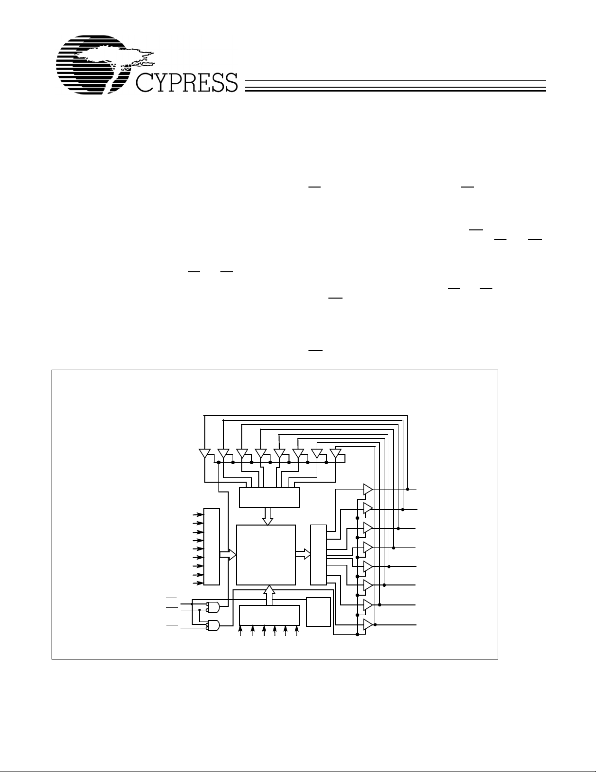
Logic Block Diagram
and OE features
Functional Description
[1]
The CY62256V family is composed of two high-performance
CMOS static RAM’s organized as 32K words by 8 bits. Easy
memory expansion is provided by an active LOW chip enable
(CE
) and active LOW output enable (OE) and three-state
drivers. These devices have an automatic power-down
feature, reducing the power consumption by over 99% when
deselected.
An active LOW write enable signal (WE
writing/reading operation of the memory. When CE
) controls the
and WE
inputs are both LOW, data on the eight data input/output pins
(I/O
through I/O7) is written into the memory location
0
addressed by the address present on the address pins (A
through A14). Reading the device is accomplished by selecting
the device and enabling the outputs, CE
while WE
remains inactive or HIGH. Under these conditions,
and OE active LOW,
the contents of the location addressed by the information on
address pins are present on the eight data input/output pins.
The input/output pins remain in a high-impedance state unless
the chip is selected, outputs are enabled, and write enable
(WE
) is HIGH.
0
I/O
I/O
I/O
I/O
I/O
I/O
I/O
I/O
0
1
2
3
4
5
6
7
INPUTBUFFER
A
10
A
9
A
8
A
7
A
6
A
5
A
4
3
2
ROW DECODER
A
A
CE
WE
OE
Note:
1. For best practice recommendations, please refer to the Cypress application note “System Design Guidelines” on http://www.cypress.com.
512 × 512
ARRA
COLUMN
DECODER
14
A13A11A
A
Y
SENSE AMPS
POWER
DOWN
0
1
12
A
A
Cypress Semiconductor Corporation • 3901 North First Street • San Jose • CA 95134 • 408-943-2600
Document #: 38-05057 Rev. *D Revised June 28, 2004
CY62256V
Product Portfolio
Power Dissipation
Product
VCC Range (V) Speed
Range Min. Typ.
[2]
Max. (ns) Typ.
Operating, ICC (mA) Standby, I
[2]
Max. Typ.
[2]
SB2
(µA)
Max.
CY62256VLL Com’l / Ind’l 2.7 3.0 3.6 70 11 30 0.1 5
CY62256VLL Automotive 2.7 3.0 3.6 70 11 30 0.1 130
CY62256V25LL Com’l 2.3 2.5 2.7 100 9 15 0.1 4
Pin Configurations
Narrow SOIC
Top View
A
A
A
A
A
A
A
A
A
A
I/O
I/O
I/O
GND
10
11
12
13
14
1
5
2
6
3
7
4
8
5
9
6
7
8
9
10
11
0
12
1
13
2
14
28
27
26
25
24
23
22
21
20
19
18
17
16
15
V
CC
WE
A
4
A
3
A
2
A
1
OE
A
0
CE
I/O
I/O
I/O
I/O
I/O
A
7
11
A
6
10
A
5
9
A
4
8
3
A
7
2
A
6
1
A
5
28
V
CC
27
WE
26
A
7
6
5
4
A
A
A
OE
4
25
3
24
2
23
1
22
TSOP I
Reverse Pinout
Top Vi e w
(not to scale)
8
A
12
9
A
13
A
10
14
11
I/O
0
12
I/O
1
13
I/O
2
14
GND
15
I/O
3
16
I/O
4
17
I/O
5
18
I/O
6
19
I/O
7
20
CE
21
A
0
OE
WE
V
A
A
A
A
A
A
CC
A
A
A
A
A
10
11
22
23
1
24
2
25
3
26
4
27
28
1
5
6
7
8
9
2
3
4
5
6
7
(not to scale)
3
Pin Definitions
Pin Number Type Description
1-10, 21, 23-26 Input A0-A14. Address Inputs
11-13, 15-19 Input/Output I/O
27 Input/Control WE
20 Input/Control CE
22 Input/Control OE
14 Ground GND. Ground for the device
28 Power Supply Vcc. Power supply for the device
Notes:
2. Typical values are included for reference only and are not guaranteed or tested. Typical values are measured at V
-I/O7. Data lines. Used as input or output lines depending on operation
0
. When selected LOW, a WRITE is conducted. When selected HIGH, a READ
is conducted
. When LOW, selects the chip. When HIGH, deselects the chip
. Output Enable. Controls the direction of the I/O pins. When LOW, the I/O pins
behave as outputs. When deasserted HIGH, I/O pins are three-stated, and act as
input data pins
TSOP I
Top V iew
= VCC Typ., TA = 25°C, and t
CC
21
A
0
20
CE
19
I/O
7
18
I/O
6
17
I/O
5
16
I/O
4
I/O
15
3
14
GND
13
I/O
2
12
I/O
1
11
I/O
0
10
A
14
9
A
13
8
A
12
= 70 ns.
AA
Document #: 38-05057 Rev. *D Page 2 of 13
CY62256V
Maximum Ratings
Static Discharge Voltage.......................................... > 2001V
(per MIL-STD-883, Method 3015)
(Above which the useful life may be impaired. For user guidelines, not tested.)
Storage Temperature .................................–65°C to +150°C
Latch-up Current.................................................... > 200 mA
Operating Range
Ambient Temperature with
Power Applied.............................................–55°C to +125°C
Supply Voltage to Ground Potential
(Pin 28 to Pin 14) ...........................................–0.5V to +4.6V
DC Voltage Applied to Outputs
in High-Z State
DC Input Voltage
[3]
....................................–0.5V to VCC + 0.5V
[3]
.................................–0.5V to VCC + 0.5V
Output Current into Outputs (LOW) .............................20 mA
Device Range
CY62256V Commercial 0°C to +70°C 2.7V to
CY62256V25 Commercial 0
Electrical Characteristics Over the Operating Range
Parameter Description Test Conditions
V
V
V
V
I
IX
I
OZ
I
CC
I
SB1
I
SB2
OH
OL
IH
IL
Output HIGH Voltage IOH = −1.0 mA V
Output LOW Voltage IOL = 2.1 mA V
Input HIGH Voltage 2.2 V
Input Leakage Voltage –0.5 0.8 V
Input Leakage Current GND < VIN < V
Output Leakage Current GND < V
VCC Operating Supply
Current
Automatic CE Power-down
Current— TTL Inputs
Automatic CE Power-down
Current— CMOS Inputs
VCC = 3.6V, I
f = f
MAX
VCC = 3.6V, CE > VIH,
V
> VIH or VIN < VIL, f = f
IN
V
= 3.6V, CE > VCC – 0.3V
CC
V
> VCC – 0.3V or VIN < 0.3V, f = 0
IN
CC
< VCC, Output Disabled Com’l, Ind’l –1 +1 µA
IN
= 0 mA,
OUT
= 1/t
RC
MAX
Ambient
Temperature
Industrial −40
Automotive −40
(TA)
+85
+125
[4]
°C to
°C
°C to
°C
V
CC
3.6V
°C to +70°C 2.3V to
2.7V
CY62256V-70
[2]
Max.
= 2.7V 2.4 V
CC
= 2.7V 0.4 V
CC
+0.3V
Com’l, Ind’l –1 +1 µA
Automotive -10 +10 µA
Automotive -10 +10 µA
All ranges 11 30 mA
All ranges 100 300 µA
Com’l 0.1 5
Ind’l 10
Automotive 130
CC
UnitMin. Typ.
V
Electrical Characteristics Over the Operating Range
CY62256V25-100
[2]
Parameter Description Test Conditions
V
OH
V
OL
V
IH
V
IL
I
IX
I
OZ
Notes:
3. V
(min.) = –2.0V for pulse durations of less than 20 ns.
IL
is the “Instant-On” case temperature
4. T
A
Output HIGH Voltage IOH = −0.1 mA Vcc=2.3V 2 V
Output LOW Voltage IOL = 0.1 mA Vcc= 2.3V 0.4 V
Input HIGH Voltage 1.7 Vcc +
Input LOW Voltage –0.3 0.7 V
Input Leakage Current GND < VIN < V
Output Leakage Current GND < V
< VCC, Output Disabled –1 +1 µA
IN
CC
–1 +1 µA
Document #: 38-05057 Rev. *D Page 3 of 13
Max.
0.3V
UnitMin. Typ.
V
Electrical Characteristics Over the Operating Range (continued)
Parameter Description Test Conditions
I
CC
I
SB1
I
SB2
Capacitance
VCC Operating Supply Current VCC = 2.7V, I
Automatic CE Power-down
Current— TTL Inputs
Automatic CE Power-down
Current — CMOS Inputs
[5]
Parameter Description Test Conditions Max. Unit
C
IN
C
OUT
Input Capacitance TA = 25°C, f = 1 MHz,
Output Capacitance 8 pF
AC Test Loads and Waveforms
V
CC
OUTPUT
INCLUDING
JIG AND
R1
50 pF
SCOPE
= 1/t
RC
V
= 2.7V, CE > VIH,
CC
> VIH or VIN < VIL, f = f
V
IN
V
= 2.7V, CE > VCC − 0.3V
CC
> VCC – 0.3V or VIN < 0.3V, f = 0
V
IN
R2
Equivalent to: THÉ VENIN EQUIVALENT
OUTPUT V
V
OUT
CC
= 3.0V
= 0 mA, f = f
V
CC
<5ns
R
th
10%
GND
CY62256V
CY62256V25-100
[2]
Com’l, Ind’l 9 15 mA
MAX
Com’l, Ind’l 75 225 µA
MAX
Com’l 0.1 4
Ind’l 8
6pF
ALL INPUT PULSES
90%
th
90%
10%
<5ns
Max.
UnitMin. Typ.
Parameter 3.3V 2.5V Units
R1 1100 16600 Ohms
R2 1500 15400 Ohms
RTH 645 8000 Ohms
VTH 1.750 1.20 Volts
Notes:
5. Tested initially and after any design or process changes that may affect these parameters.
Document #: 38-05057 Rev. *D Page 4 of 13

Data Retention Characteristics (Over the Operating Range)
Parameter Description Conditions
V
DR
I
CCDR
[6]
t
CDR
[6]
t
R
Data Retention Waveform
V
CC
CE
Thermal Resistance
VCC for Data Retention 1.4 V
Data Retention Current VCC = 1.6V, CE > VCC – 0.3V,
V
> VCC – 0.3V or VIN < 0.3V
IN
Chip Deselect to Data
Retention Time
Operation Recovery Time t
DATA RETENTION MODE
VDR> 1.4V
t
CDR
[6]
CY62256V
Min. Typ.
Com’l 0.1 3 µA
Ind’l 6
Auto 50
0ns
RC
1.8V1.8V
t
R
[2]
Max. Unit
ns
Parameter Description Test Conditions SOIC TSOPI RTSOPI Unit
Θ
Θ
Notes:
6. No input may exceed V
Thermal Resistance
JA
(Junction to Ambient)
Thermal Resistance
JC
(Junction to Case)
CC
+ 0.3V.
Still Air, soldered on a 3 × 4.5 inch,
[6]
four-layer printed circuit board
[5]
68.45 87.62 87.62 °C/W
26.94 23.73 23.73 °C/W
Document #: 38-05057 Rev. *D Page 5 of 13

CY62256V
Switching Characteristics Over the Operating Range
[7]
CY62256V-70 CY62256V25-100
Parameter Description
Read Cycle
t
RC
t
AA
t
OHA
t
ACE
t
DOE
t
LZOE
t
HZOE
t
LZCE
t
HZCE
t
PU
t
PD
Write Cycle
t
WC
t
SCE
t
AW
t
HA
t
SA
t
PWE
t
SD
t
HD
t
HZWE
t
LZWE
Notes:
7. Test conditions assume signal transition time of 5 ns or less timing reference levels of V
I
8. At any given temperature and voltage condition, t
9. t
10. The internal write time of the memory is defined by the overlap of CE
a write by going HIGH. The data input set-up and hold timing should be referenced to the rising edge of the signal that terminates the write.
11. The minimum write cycle time for write cycle #3 (WE
[10, 11]
and 100-pF load capacitance.
OL/IOH
, t
HZCE
, and t
HZWE
HZOE
are specified with CL = 5 pF as in (b) of AC Test Loads. Transition is measured ± 200 mV from steady-state voltage.
Read Cycle Time 70 100 ns
Address to Data Valid 70 100 ns
Data Hold from Address Change 10 10 ns
CE LOW to Data Valid 70 100 ns
OE LOW to Data Valid 35 75 ns
OE LOW to Low-Z
OE HIGH to High-Z
CE LOW to Low-Z
CE HIGH to High-Z
[8]
[8]
[8, 9]
[8, 9]
55ns
25 50 ns
10 10 ns
25 50 ns
CE LOW to Power-up 0 0 ns
CE HIGH to Power-down 70 100 ns
Write Cycle Time 70 100 ns
CE LOW to Write End 60 90 ns
Address Set-up to Write End 60 90 ns
Address Hold from Write End 0 0 ns
Address Set-up to Write Start 0 0 ns
WE Pulse Width 50 80 ns
Data Set-up to Write End 30 60 ns
Data Hold from Write End 0 0 ns
WE LOW to High-Z
WE HIGH to Low-Z
HZCE
[8, 9]
[8]
is less than t
controlled, OE LOW) is the sum of t
, t
LZCE
is less than t
HZOE
LOW and WE LOW. Both signals must be LOW to initiate a write and either signal can terminate
25 50 ns
10 10 ns
/2, input pulse levels of 0 to VCC, and output loading of the specified
CC
HZWE
LZOE
and tSD.
, and t
HZWE
is less than t
for any given device.
LZWE
UnitMin. Max. Min. Max.
Document #: 38-05057 Rev. *D Page 6 of 13

Switching Waveforms
Read Cycle No. 1
ADDRESS
DATA OUT PREVIOUS DATA VALID
[12, 13]
t
OHA
t
RC
t
AA
CY62256V
DATA VALID
Read Cycle No. 2
[13, 14]
CE
OE
DATA OUT
V
CC
SUPPLY
HIGH IMPEDANCE
t
LZCE
t
PU
CURRENT
Write Cycle No.1 (WE Controlled)
ADDRESS
CE
t
ACE
t
DOE
t
LZOE
50%
[10, 15, 16]
t
RC
t
HZOE
t
DATA VALID
HZCE
t
PD
HIGH
IMPEDANCE
ICC
50%
ISB
t
WC
t
HA
WE
t
AW
t
SA
t
PWE
OE
DATA I/O
Notes:
12. Device is continuously selected. OE
is HIGH for read cycle.
13. WE
NOTE 17
t
HZOE
, CE = VIL.
t
SD
DATAINVALID
t
HD
Document #: 38-05057 Rev. *D Page 7 of 13

Switching Waveforms (continued)
Write Cycle No. 2 (CE Controlled)
ADDRESS
[10, 15, 16]
t
WC
CY62256V
CE
t
SA
t
AW
WE
DATA I/O
Write Cycle No. 3 (WE Controlled, OE LOW)
[11, 16]
t
WC
ADDRESS
CE
t
AW
t
SA
WE
DATA I/O
Notes:
14. Address valid prior to or coincident with CE
15. Data I/O is high impedance if OE = VIH.
16. If CE
17. During this period, the I/Os are in output state and input signals should not be applied.
goes HIGH simultaneously with WE HIGH, the output remains in a high-impedance state.
NOTE 17
t
HZWE
transition LOW.
t
SCE
t
SD
DATAINVALID
t
SD
DATAINVALID
t
HA
t
HD
t
HA
t
HD
t
LZWE
Document #: 38-05057 Rev. *D Page 8 of 13

Typical DC and AC Characteristics
NORMALIZED SUPPLY CURRENT
vs. SUPPLY VOLTAGE
1.8
1.6
1.4
CC
1.2
CC
1.0
0.8
0.6
NORMALIZED I
0.4
TA= 25°C
NORMALIZED I
0.2
2.4
2.0
1.8
1.6
SUPPLY VOLTAGE (V)
2.8
3.2
3.6
NORMALIZED ACCESS TIME
vs. SUPPLY
VOLTAGE
2.5
2.0
AA
AA
1.5
TA = 25°C
1.0
NORMALIZED t
NORMALIZED t
0.5
0.0
1.65 2.1 2.6 3.1 3.6
SUPPLY VOLTAGE (V)
NORMALIZED SUPPLY CURRENT
vs. AMBIENT TEMPERATURE
1.4
1.2
1.0
0.8
VCC = 2.5V
0.6
0.4
0.2
0.0
−55 25 125
AMBIENT TEMPERATURE (°C)
NORMALIZED ACCESS TIME
vs. AMBIENT TEMPERATURE
1.6
1.4
VCC = 2.5V
1.2
1.0
0.8
0.6
−55 25 125
AMBIENT TEMPERATURE (°C)
OUTPUT SOURCE CURRENT
vs. OUTPUT VOLTAGE
-14
VCC = 3.0V
VCC = 3.0V
CY62256V
STANDBY
vs. AMBIENT TEMPERATURE
3.0
2.5
2.0
1.5
µA
1.0
SB2
I
0.5
I
SB
0.0
-0.5
−55 25 105
AMBIENT TEMPERATURE (°C)
OUTPUT SINK CURRENT
vs. OUTPUT VOLTAGE
14
12
10
8
6
4
2
OUTPUT SINK CURRENT (mA)
0
0.0 1.0
OUTPUT VOLTAGE (V)
CURRENT
= 2.5 V
V
CC
TA = 25°C
.3
3
=
cc
V
= 2
cc
V
2.0 3.0
V
5V
.
-12
-10
-8
= 2.5V
V
-6
CC
T
= 25°C
A
-4
0
OUTPUT SOURCE CURRENT (mA)
0.5
0.0 1.0
1.5
22.5
OUTPUT VOLTAGE (V)
Document #: 38-05057 Rev. *D Page 9 of 13

Typical DC and AC Characteristics (continued)
CY62256V
TYPICAL ACCESS TIME CHANGE
vs. OUTPUT LOADING
30.0
25.0
TA = 25°C
= 3V
V
CC
20.0
AA
15.0
DELTA t (ns)
10.0
5.0
0.0
0 200 400 600 800
CAPACITANCE (pF)
1000
NORMALIZED I
1.25
CC
1.00
0.75
NORMALIZED I
0.50
1
vs.CYCLETIME
CC
VCC = 3.0V
TA = 25°C
V
= 0.5V
IN
10
CYCLE FREQUENCY (MHz)
20 30
Truth Table
CE WE OE
H X X High-Z Deselect/Power-down Standby (I
L H L Data Out Read Active (ICC)
L L X Data In Write Active (I
L H H High-Z Deselect, Output Disabled Active (I
Inputs/Outputs Mode Power
)
SB
)
CC
)
CC
Ordering Information
Speed
(ns) Ordering Code
70 CY62256VLL-70SNC SN28 28-lead (300-mil Narrow Body) Narrow SOIC Commercial
CY62256VLL-70ZC Z28 28-lead Thin Small Outline Package
CY62256VLL-70ZI Industrial
CY62256VLL -70SNI SN28 28-lead (300-mil Narrow Body) Narrow SOIC
CY62256VLL-70ZRI ZR28 28-lead Reverse Thin Small Outline Package
CY62256VLL-70SNE SN28 28-lead (300-mil Narrow Body) Narrow SOIC Automotive
CY62256VLL-70ZE Z28 28-lead Thin Small Outline Package
CY62256VLL-70ZRE ZR28 28-lead Reverse Thin Small Outline Package
100 CY62256V25LL-100ZC Z28 28-lead Thin Small Outline Package Commercial
Package
Name Package Type
Operating
Range
Document #: 38-05057 Rev. *D Page 10 of 13

Package Diagrams
28-lead (300-mil) SNC (Narrow Body) SN28
CY62256V
51-85092-*B
28-lead Thin Small Outline Package Type 1 (8 × 13.4 mm) Z28
51-85071-*G
Document #: 38-05057 Rev. *D Page 11 of 13

Package Diagrams (continued)
28-lead Reverse Type 1 Thin Small Outline Package (8 × 13.4 mm) ZR28
CY62256V
All product and company names mentioned in this document are the trademarks of their respective holders.
51-85074-*F
Document #: 38-05057 Rev. *D Page 12 of 13
© Cypress Semiconductor Corporation, 2004. The information contained herein is subject to change without notice. Cypress Semiconductor Corporation assumes no responsibility for the use
of any circuitry other than circuitry embodied in a Cypress product. Nor does it convey or imply any license under patent or other rights. Cypress products are not warranted nor intended to be
used for medical, life support, life saving, critical control or safety applications, unless pursuant to an express written agreement with Cypress. Furthermore, Cypress does not authorize its
products for use as critical components in life-support systems where a malfunction or failure may reasonably be expected to result in significant injury to the user. The inclusion of Cypress
products in life-support systems application implies that the manufacturer assumes all risk of such use and in doing so indemnifies Cypress against all charges.

Document Title: CY62256V 256K (32K x 8) Static RAM
Document Number: 38-05057
REV. ECN NO. Issue Date
** 107248 09/10/01 SZV Changed from spec number: 38-00519 to 38-05057
*A 111445 11/01/01 MGN Removed obsolete parts. Change to standard format
*B 115229 05/23/02 GBI Changed SN package diagram
*C 116507 09/04/02 GBI Added footnote 1
*D 239134 See ECN AJU Added Automotive product information
Orig. of
Change Description of Change
Clarified I
spec for V
CC
CC(typ)
= 2.5V
CY62256V
Document #: 38-05057 Rev. *D Page 13 of 13
 Loading...