

Page 1
CY62256
256K (32K x 8) Static RAM
Features
• High speed: 55 ns and 70 ns
• Voltage range: 4.5V–5.5V operation
• Low active power (70 ns, LL version)
—275 mW (max.)
• Low standby power (70 ns, LL version)
—28 µW (max.)
• Easy memory expansion with C E
• TTL-compatible inputs and outputs
• Automatic power-down when deselec ted
• CMOS for optimum speed/power
• Package available in a standard 450 -mil -wi de (300-m il
body width) 28-lead narrow SOIC, 28-lead TSOP-1,
28-lead reverse TSOP-1, and 600-mil 28-lead PDIP
packages
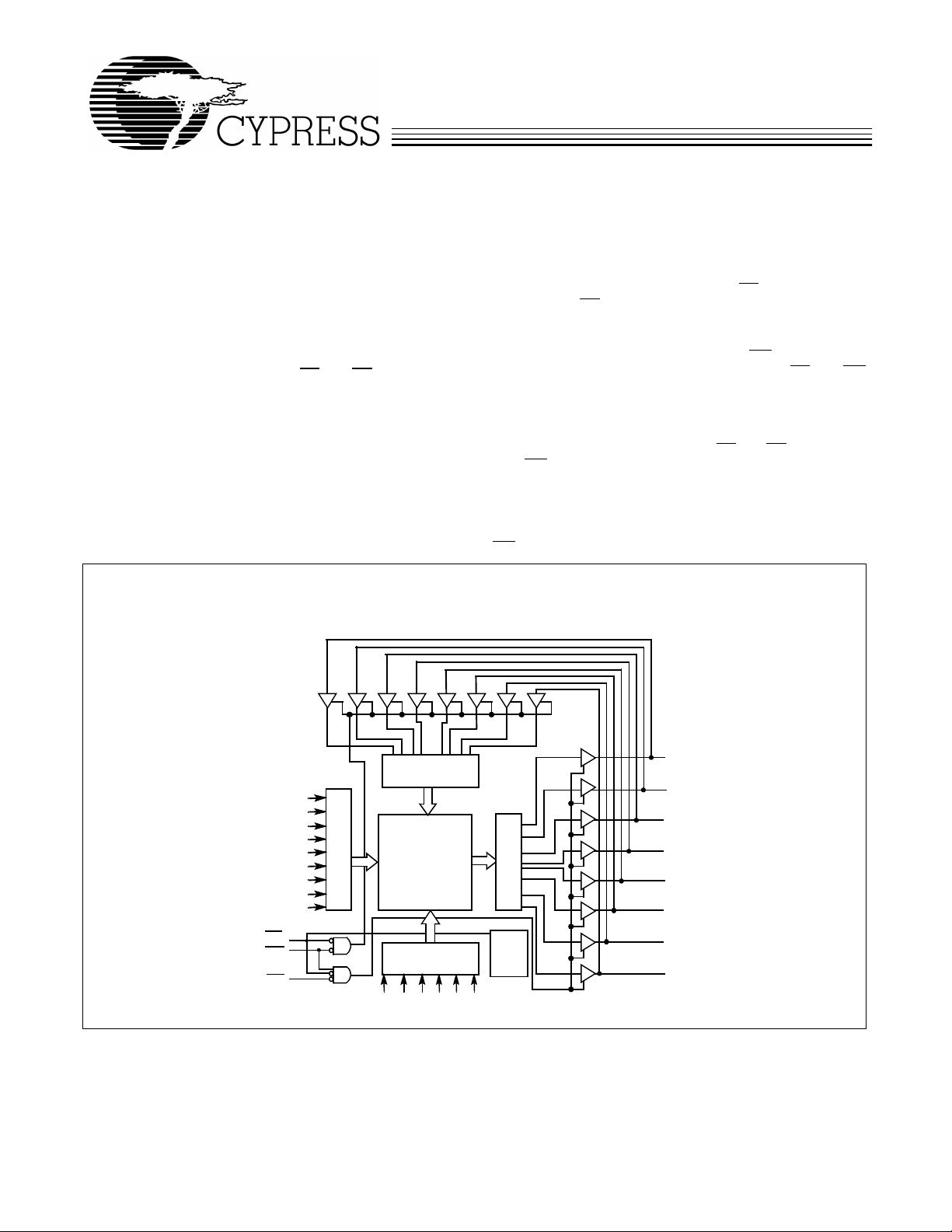
Logic Block Diagram
and OE features
Functional Description
[1]
The CY62256 is a high-performance CMOS static RAM
organized as 32K words by 8 bits . E asy m em ory e xpansion is
provided by an acti ve LOW chip enable (CE
output enable (OE
) and three-stat e drivers. Thi s device has an
) and active LOW
automatic power-down feature, reducing the power
consumption by 99.9% when deselected.
An active LOW write enable signal (WE
writing/reading operation of the memory. When CE
) controls the
and WE
inputs are both LOW, data on the eight data input/output pins
through I/O7) is written into the memory location
(I/O
0
addressed by the address present on the address pins (A
through A14). Reading the device is acc omplished by selecti ng
the device and enabling the outputs, CE and OE active LOW,
while WE
remains ina ctive or HIGH . Unde r thes e condi tions ,
the contents of the location addressed by the information on
address pins are present on the eight data input /output pins.
The input/output pi ns remain in a high-i mpedance st ate unless
the chip is selected, outputs are enabled, and write enable
) is HIGH.
(WE
0
I/O
I/O
I/O
I/O
I/O
I/O
I/O
I/O
0
1
2
3
4
5
6
7
INPUTBUFFER
A
10
A
9
A
8
A
7
A
6
A
5
A
4
A
A
CE
WE
OE
Note:
1. For best practice recommendations, please refer to the Cypress application note “System Design Guidelines” on http://www.cypress.com.
ROW DECODER
3
2
512 x 512
ARRA
COLUMN
DECODER
14
A
A13A11A
Y
SENSE AMPS
POWER
DOWN
0
1
12
A
A
Cypress Semiconductor Corporation • 3901 North First Street • San Jose • CA 95134 • 408-943-2600
Document #: 38-05248 Rev. *B Revised August 27, 2002
Page 2
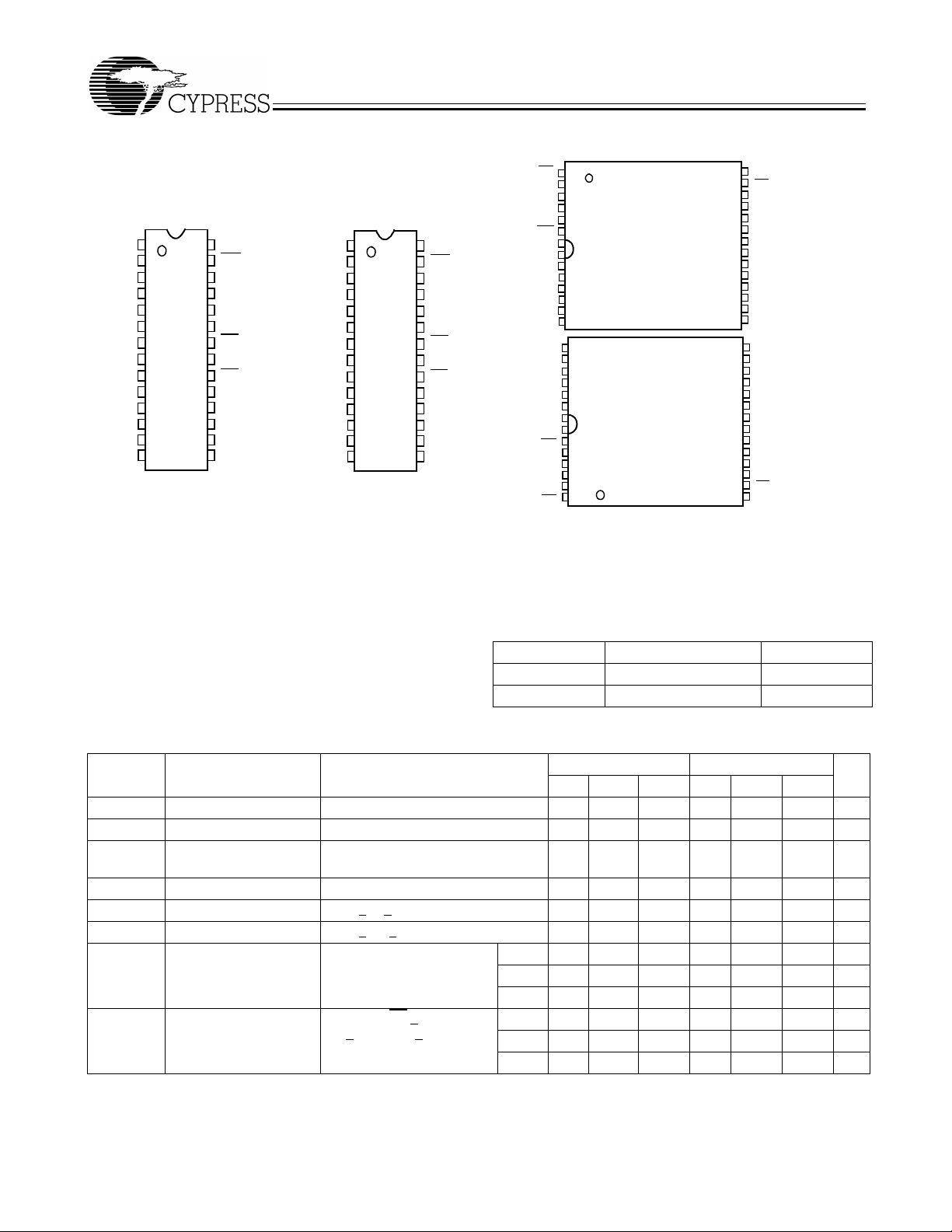
Pin Configurations
Narrow SOIC
Top View
A
A
A
A
A
A
10
A
11
A
12
A
13
A
14
I/O
I/O
I/O
GND
5
6
7
8
9
0
1
2
1
2
3
4
5
6
7
8
9
10
11
12
13
14
28
27
26
25
24
23
22
21
20
19
18
17
16
15
V
CC
WE
A
4
A
3
A
2
A
1
OE
A
0
CE
I/O
I/O
I/O
I/O
I/O
A
A
A
A
7
6
5
4
3
A
I/O
I/O
I/O
GND
Maximum Ratings
(Above which the us efu l l ife may be impaired. F or us er gui delines, not tested.)
Storage Temperature .................................–65°C to +150°C
Ambient Temperature with
Power Applied...................................................0°C to +70°C
Supply Voltage to Ground Potential
(Pin 28 to Pin 14)...........................................–0.5V to +7.0V
DC Voltage Applied to Outputs
in High-Z State
[2]
....................................–0.5V to VCC + 0.5V
A
5
A
6
A
7
A
8
A
9
10
11
12
13
14
0
1
2
DIP
Top View
28
1
27
2
26
3
4
25
24
5
23
6
22
7
21
8
20
9
19
10
18
11
17
12
16
13
15
14
V
CC
WE
A
4
A
3
A
2
A
1
OE
A
0
CE
I/O
I/O
I/O
I/O
I/O
7
6
5
4
3
CY62256
21
22
OE
A
23
1
A
24
2
A
25
3
A
26
4
27
WE
28
V
CC
A
1
5
A
2
6
3
A
7
A
4
8
5
A
9
A
6
10
A
7
11
A
7
11
A
6
10
A
5
9
A
4
8
3
A
7
2
A
6
1
A
5
28
V
CC
27
WE
26
A
4
A
25
3
24
A
2
23
A
1
22
OE
DC Input Voltage
TSOP I
Top View
(not to scale)
TSOP I
Reverse Pinout
Top View
(not to scale)
[2]
................................–0.5V to VCC + 0.5V
Output Current into Outputs (LOW).............................20 mA
Static Discharge Voltage.......................................... > 2001V
(per MIL-STD-883, Method 3015)
Latch-up Current.................................................... > 200 mA
Operating Range
Range Ambient Temperature V
Commercial 0°C to +70°C 5V ± 10%
Industrial –40°C to +85°C 5V ± 10%
A
0
20
CE
19
I/O
7
18
I/O
6
17
I/O
5
16
I/O
4
I/O
15
3
14
GND
13
I/O
2
12
I/O
1
11
I/O
0
10
A
14
9
A
13
8
A
12
8
A
12
9
A
13
A
10
14
11
I/O
0
12
I/O
1
13
I/O
2
14
GND
15
I/O
3
16
I/O
4
17
I/O
5
18
I/O
6
19
I/O
7
20
CE
21
A
0
CC
Electrical Characteristics Over the Operating Range
CY62256−55
Parameter Description Test Conditions
V
OH
V
OL
V
IH
V
IL
I
IX
I
OZ
I
CC
Output HIGH Voltage VCC = Min., IOH = −1.0 mA 2.4 2.4 V
Output LOW Voltage VCC = Min., IOL = 2.1 mA 0.4 0.4 V
Input HIGH Voltage 2.2 V
Input LOW Voltage –0.5 0.8 –0.5 0.8 V
Input Leakage Current GND < VI < V
CC
Output Leakage Current GND < VO < VCC, Output Disabled –0.5 +0.5 –0.5 +0.5 µA
VCC Operating Supply
Current
VCC = Max., I
= 1/t
f = f
MAX
OUT
RC
= 0 mA,
–0.5 +0.5 –0.5 +0.5 µA
L255025 50 mA
[3]
Max. Min. Typ.
CC
+0.5V
28 55 28 55 mA
LL 25 50 25 50 mA
I
SB1
Automatic CE
Power-down Current—
TTL Inputs
Max. VCC, CE > VIH,
> VIH or VIN < VIL, f = f
V
IN
0.5 2 0.5 2 mA
MAX
L0.40.60.4 0.6 mA
LL 0.3 0.5 0.3 0.5 mA
Notes:
2. V
(min.) = −2.0V for pulse durations of less than 20 ns.
IL
3. Typical specifications are the mean values measured over a large sample size across normal production process variations and are taken at no minal cond itio ns
= 25°C, VCC). Parameters are guaranteed by design and characterization, and not 100% tested.
(T
A
Document #: 38-05248 Rev. *B Page 2 of 11
CY62256−70
[3]
Max.
2.2 V
+0.5V
CC
UnitMin. Typ.
V
Page 3
Electrical Characteristics Over the Operating Range (continued)
Parameter Description Test Conditions
I
SB2
Capacitance
C
IN
C
OUT
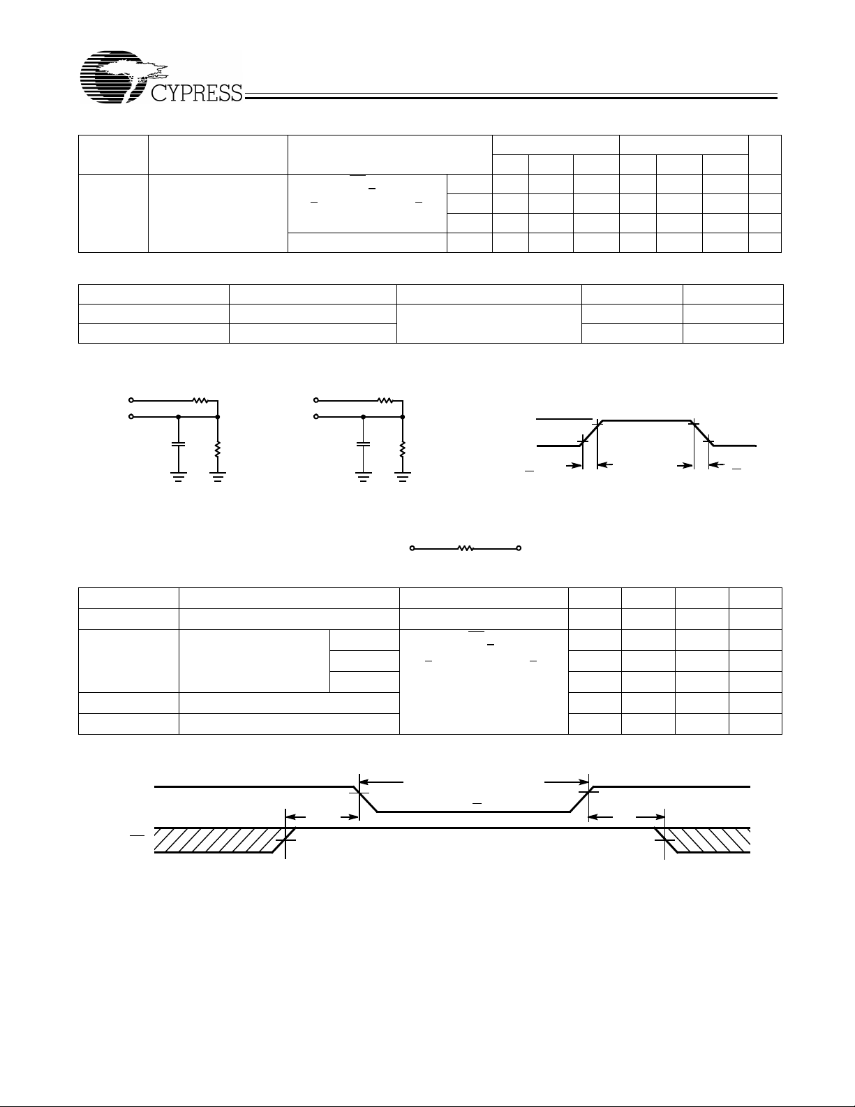
AC Test Loads and Waveforms
OUTPUT
INCLUDING
Automatic CE
Power-down Current—
CMOS Inputs
Max. VCC, CE > VCC − 0.3V
> VCC − 0.3V , or VIN <
V
IN
0.3V, f = 0
L2502 50 µA
LL 0.1 5 0.1 5 µA
Indust’l Temp R ang e LL 0.1 10 0.1 10 µA
[4]
Parameter Description Test Conditions Max. Unit
Input Capacitance TA = 25°C, f = 1 MHz,
= 5.0V
V
5V
100 pF
JIG AND
SCOPE
Output Capacitance 8 pF
R1 1800
Ω
R2
990Ω
(a) (b)
5V
OUTPUT
5pF
INCLUDING
JIG AND
SCOPE
Equivalent to: THÉ VENIN EQUIVALENT
OUTPUT 1.77V
R1 1800
CC
Ω
R2
990Ω
639Ω
CY62256−55 CY62256−70
[3]
Max. Min. Typ.
15 1 5 mA
6 pF
3.0V
GND
10%
<5ns
ALL INPUT PULSES
90%
CY62256
[3]
Max.
90%
10%
<5ns
UnitMin. Typ.
Data Retention Characteristics
Parameter Description Conditions
V
DR
I
CCDR
VCC for Data Retention 2.0 V
Data Retention Current L VCC = 3.0V, CE > VCC − 0.3V,
V
> VCC − 0. 3V, or VIN < 0.3V
LL 0.1 5 µA
IN
LL Ind’l 0.1 10 µA
[4]
t
CDR
t
R
[4]
Chip Deselect to Data Retention Time 0 ns
Operation Recovery Time t
Data Retention Waveform
DATA RETENTION MODE
V
CC
t
CDR
CE
Notes:
4. Tested initially and after any design or process changes that may affect these parameters.
5. No input may exceed V
CC
+ 0.5V .
VDR> 2V
[5]
Min. Typ.
[3]
Max. Unit
2 50 µA
RC
3.0V3.0V
t
R
ns
Document #: 38-05248 Rev. *B Page 3 of 11
Page 4
CY62256
Switching Characteristics Over the Operating Range
Parameter Description
Read Cycle
t
RC
t
AA
t
OHA
t
ACE
t
DOE
t
LZOE
t
HZOE
t
LZCE
t
HZCE
t
PU
t
PD
Write Cycle
t
WC
t
SCE
t
AW
t
HA
t
SA
t
PWE
t
SD
t
HD
t
HZWE
t
LZWE
[9, 10]
Read Cycle Time 55 70 ns
Address to Data Valid 55 70 ns
Data Hold from Address Change 5 5 ns
CE LOW to Data Valid 55 70 ns
OE LOW to Data Valid 25 35 ns
OE LOW to Low-Z
OE HIGH to High-Z
CE LOW to Low-Z
CE HIGH to High-Z
[7]
[7, 8]
[7]
[7, 8]
CE LOW to Power-up 0 0 ns
CE HIGH to Power-down 55 70 ns
Write Cycle Time 55 70 ns
CE LOW to Write End 45 60 ns
Address Set-up to Write End 45 60 ns
Address Hold from Write End 0 0 ns
Address Set-up to Write Start 0 0 ns
WE Pulse Width 40 50 ns
Data Set-up to Write End 25 30 ns
Data Hold from Write End 0 0 ns
WE LOW to High-Z
WE HIGH to Low-Z
[7, 8]
[7]
[6]
CY62256−55
CY62256−70
UnitMin. Max. Min. Max.
5 5 ns
20 25 ns
5 5 ns
20 25 ns
20 25 ns
5 5 ns
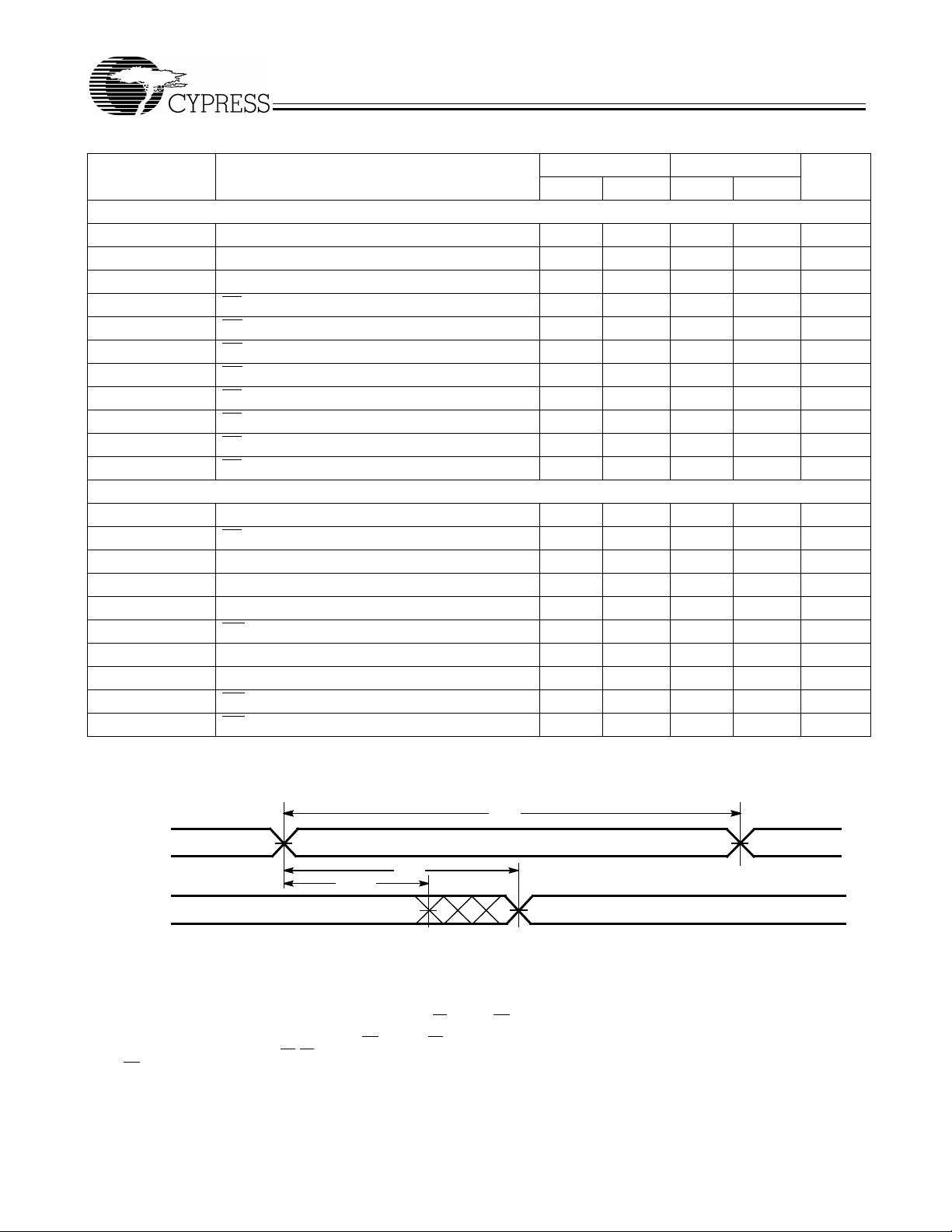
Switching Waveforms
, and t
[11, 12]
t
RC
t
t
OHA
are specified with CL = 5 pF as in (b) of AC Test Loads. Transition is me asured ±500 mV from ste ady-st ate volt age.
HZWE
AA
is less than t
HZCE
controlled, OE L OW) is the sum of t
, t
LZCE
HZOE
LOW and WE LOW . Both signals must be LOW to initiate a Write and either signal can terminate
is less than t
LZOE
HZWE
, and t
and t
HZWE
SD
is less than t
DATA VALID
for any given de vice .
LZWE
Read Cycle No. 1
ADDRESS
DATA OUT PREVIOUS DATA VALID
Notes:
6. T est conditions assume signal transition time of 5 ns or less, timing reference levels of 1.5V, input pulse levels of 0 to 3.0V, and output loading of the specified
I
and 100-pF load cap acit ance.
OL/IOH
7. At any given temperature and voltage condition, t
8. t
9. The inter nal W rit e time o f the memory i s defi ned by t he ov erlap o f C E
10. The minimum Write cycle time for Write cycle #3 (WE
11. Device is continuously selected. OE, CE = VIL.
12. WE
, t
HZOE
HZCE
a Write by goi ng HIGH. The dat a in put se t-up a nd hold t iming s hould be ref erenced to the r ising edge of the s ignal t hat termi nates the Write.
is HIGH for Read cycle.
Document #: 38-05248 Rev. *B Page 4 of 11
Page 5

Switching Waveforms (continued)
Read Cycle No. 2
CE
OE
DATA OUT
V
CC
SUPPLY
CURRENT
[12, 13]
HIGH IMPEDANCE
t
LZCE
t
PU
t
ACE
t
LZOE
t
DOE
50%
t
RC
t
HZOE
t
HZCE
DATA VALID
t
CY62256
HIGH
IMPEDANCE
PD
ICC
50%
ISB
Write Cycle No. 1 (WE Controlled)
ADDRESS
CE
t
WE
SA
OE
DATA I/O
NOTE
16
t
HZOE
Write Cycle No. 2 (CE Controlled)
ADDRESS
CE
[9, 14, 15]
[9, 14, 15]
t
SA
t
AW
t
AW
t
t
WC
WC
t
PWE
t
SD
DATAINVALID
t
SCE
t
HA
t
HD
t
HA
WE
t
HD
DATA I/O
Notes:
13. Address valid prior to or coincident with CE
14. Data I/O is high impedance if OE
15. If CE
goes HIGH simultaneously wit h WE HIGH, the ou tput remains in a h igh-impeda nce s tat e.
= VIH.
transition LOW .
t
SD
DATAINVALID
Document #: 38-05248 Rev. *B Page 5 of 11
Page 6

Switching Waveforms (continued)
Write Cycle No. 3 (WE Controlled, OE LOW)
ADDRESS
CE
[10, 15]
t
CY62256
WC
t
AW
t
WE
DATA I/O
Note:
16. During this period, the I/Os are in output state and input signals should not be applied.
SA
NOTE 16
t
HZWE
t
SD
DATAINVALID
t
HA
t
LZWE
t
HD
Document #: 38-05248 Rev. *B Page 6 of 11
Page 7

Typical DC and AC Characteristics
NORMALIZED SUPPLY CURRENT
vs. SUPPLY VOLTAGE
1.4
1.2
I
1.0
CC SB
0.8
0.6
0.4
NORMALIZED I , I
0.2
I
SB
0.0
4.0 4.5 5.0 5.5 6.0
NORMALIZED ACCESS TIME
vs. SUPPLY
1.4
1.3
AA
1.2
1.1
1.0
NORMALIZED t
0.9
0.8
4.0 4.5 5.0 5.5 6.0
CC
=5.0V
V
IN
T
=25°C
A
SUPPLY VOLTAGE (V)
VOLTAGE
TA=25°C
SUPPLYVOLTAGE (V)
CC
NORMALIZED I
AA
NORMALIZED t
NORMALIZED SUPPLY CURRENT
vs. AMBIENT TEMPERATURE
1.4
1.2
1.0
0.8
0.6
0.4
0.2
0.0
−55 25 125
NORMALIZED ACCESS TIME
vs. AMBIENT TEMPERATURE
1.6
1.4
1.2
1.0
0.8
0.6
−55 25 125
120
I
CC
=5.0V
V
CC
=5.0V
V
IN
AMBIENT TEMPERATURE (°C)
VCC=5.0V
AMBIENT TEMPERATURE (°C)
OUTPUT SOURCE CURRENT
vs. OUTPUT
VOLTAGE
CY62256
STANDBY
vs. AMBIENT TEMPERATURE
3.0
2.5
2.0
1.5
µA
1.0
SB2
I
0.5
0.0
-0.5
−55 25 105
AMBIENT TEMPERATURE (°C)
OUTPUT SINK CURRENT
vs. OUTPUT VOLTAGE
140
120
100
80
60
40
20
OUTPUT SINK CURRENT (mA)
0
0.0 1.0 2.0 3.0 4.0
OUTPUT VOLTAGE (V)
CURRENT
VCC=5.0V
V
IN
=5.0V
V
CC
T
=25°C
A
I
SB
=5.0V
100
80
V
=5.0V
60
CC
T
A
=25°C
40
20
0
OUTPUT SOURCE CURRENT (mA)
0.0 1.0 2.0 3.0 4.0
OUTPUT VOLTAGE (V)
Document #: 38-05248 Rev. *B Page 7 of 11
Page 8

Typical DC and AC Characteristics (continued)
CY62256
TYPICAL POW ER-ON CURRENT
vs. SUPPLY
3.0
2.5
PO
2.0
1.5
1.0
NORMALIZED I
0.5
0.0
0.0 1.0 2.0 3.0 4.0
VOLTAGE
SUPPLYVOLTAGE (V)
5.0
TYPICAL ACCESS TIME CHANGE
vs. OUTPUT LOADING
30.0
25.0
20.0
AA
15.0
DELTA t (ns)
10.0
5.0
0.0
0 200 400 600 800
CAPACITANCE (pF)
V
CC
T
A
=4.5V
=25°C
1000
NORMALIZED I
1.25
=5.0V
V
CC
1.00
0.75
NORMALIZED I
0.50
10 20 30 40
CC
T
=25°C
A
=0.5V
V
IN
CYCLE FREQUENCY (MHz)
vs.CYCLETIME
CC
Truth Table
CE WE OE Inputs/Outputs Mode Power
H X X High-Z Deselect/Power-down Standby (ISB)
L H L Data Out Read Active (ICC)
L L X Data In Write Active (ICC)
L H H High-Z Deselect, Output Disabled Active (ICC)
Ordering Information
Speed
(ns) Ordering Code
55 CY62256LL−55SNI SN28 28-lead (300-Mil Narrow Body) Narrow SOIC Industrial
CY62256LL−55ZI Z28 28-lead Thin Small Outline Package
70 CY62256−70SNC SN28 28-lead (300-Mil Narrow Body) Narrow SOIC Commercial
CY62256L−70SNC
CY62256LL−70SNC
CY62256L–70SNI Industrial
CY62256LL−70SNI
CY62256LL−70ZC Z28 28-lead Thin Small Outline Packa ge Commercial
CY62256LL−70ZI Z28 Industrial
CY62256−70PC P15 28-l ead (600-Mil) Molded DIP Commercial
CY62256L−70PC P15
CY62256LL−70PC P15
CY62256LL−70ZRI ZR28 28-lead R everse Thin Small Outline Package
Package
Name Package Type
Operating
Range
Industrial
Document #: 38-05248 Rev. *B Page 8 of 11
Page 9

Package Diagrams
28-lead (600-mil)Molded DIP P15
28-lead (300-mil) SNC (Narrow Body) SN28
CY62256
51-85017-A
51-85092-*B
Document #: 38-05248 Rev. *B Page 9 of 11
Page 10

Package Diagrams (continued)
28-lead Thin Small Outline Package Type 1 (8 x 13.4 mm) Z28
CY62256
28-lead Reverse Type 1 Thin Small Outline Package (8 x 13.4 mm) ZR28
51-85071-*G
51-85074-*F
All product and company names mentioned in this document are the trademarks of their respective holders.
Document #: 38-05248 Rev. *B Page 10 of 11
© Cypress Semiconductor Corporation, 2002. The information contained herein is subject to change without notice. Cypress Semiconductor Corporation assumes no responsibility for the use
of any circuitry other than cir cuitry embodi ed in a Cypress S emiconductor product . Nor does it convey or imply any license un der patent or other righ ts. Cypre ss Semiconductor does not autho rize
its products for use as critical components in life-support systems where a malfunction or failure may reasonably be expected to result in significant injury to the user. The inclusion of Cypress
Semiconductor products in life-support systems application implies that the manufacturer assumes all risk of such use and in doing so indemnifies Cypress Semiconductor against all charges.
Page 11

Document Title: CY62256 256K (32K x 8) Static RAM
Document Number: 38-05248
REV. ECN NO.
** 113454 03/06/02 MGN Change from Spec number: 38-00455 to 38-05248
*A 115227 05/23/02 GBI Changed SN Package Diagram
*B 116506 09/04/02 GBI Added footnote 1.
Issue
Date
Orig. of
Change Description of Change
Remove obsolete parts from ordering info, standardiz e format
Corrected package description in Ordering Information tab le
CY62256
Document #: 38-05248 Rev. *B Page 11 of 11
 Loading...