

Page 1
16-Mbit (1M x 16 / 2M x 8) Static RAM
Features
• Configurable as 1M x 16 or as 2M x 8 SRAM
• Very high speed: 45 ns
• Wide voltage range: 4.5V–5.5V
• Ultra low standby power
— Typical standby current: 1.5 µA
— Maximum standby current: 12 µA
• Ultra low active power
— Typical active current: 2.2 mA @ f = 1 MHz
• Easy memory expansion with CE
• Automatic power down when deselected
• CMOS for optimum speed and power
• Offered in 48-pin TSOP I package
Functional Description
The CY62167E is a high performance CMOS static RAM
organized as 1M words by 16 bits/2M words by 8 bits. This
device features advanced circuit design to provide an ultra low
active current. This is ideal for providing More Battery Life™
®
(MoBL
) in portable applications such as cellular telephones.
The device also has an automatic power down feature that
reduces power consumption by 99% when addresses are not
toggling. Place the device into standby mode when deselected
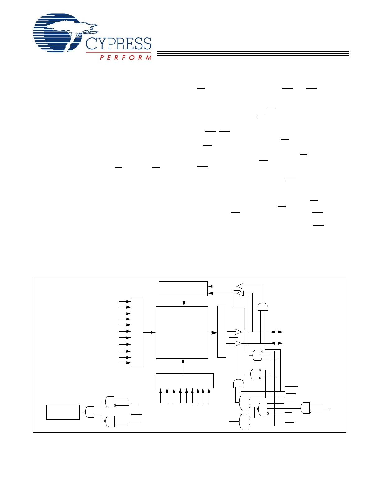
Logic Block Diagram
, CE2, and OE features
1
[1]
CY62167E MoBL
(CE
HIGH, or CE2 LOW, or both BHE and BLE are HIGH).
1
The input and output pins (IO
high impedance state when:
• The device is deselected (CE
• Outputs are disabled (OE
• Both Byte High Enable and Byte Low Enable are disabled
, BLE HIGH) or
(BHE
• A write operation is in progress (CE
WE
LOW)
To write to the device, take Chip Enables (CE
HIGH) and Write Enable (WE) input LOW. If Byte Low Enable
) is LOW, then data from IO pins (IO0 through IO7), is
(BLE
written into the location specified on the address pins (A
through A19). If Byte High Enable (BHE) is LOW, then data
from the IO pins (IO
specified on the address pins (A
through IO15) is written into the location
8
To read from the device, take Chip Enables (CE
CE
HIGH) and Output Enable (OE) LOW while forcing the
2
Write Enable (WE
) HIGH. If Byte Low Enable (BLE) is LOW,
then data from the memory location specified by the address
pins appears on IO0 to IO7. If Byte High Enable (BHE) is LOW,
then data from memory appears on IO
Table” on page 10 for a complete description of read and write
modes.
through IO15) are placed in a
0
HIGH or CE2 LOW)
1
HIGH)
LOW, CE2 HIGH, and
1
LOW and CE
1
through A19).
0
LOW and
1
to IO15. See the “Truth
8
®
2
0
DATA IN DRIVERS
A
10
A
9
A
8
A
7
A
A
A
A
A
A
A
6
5
4
3
2
1
0
ROW DECODER
1M × 16 / 2M x 8
RAM ARRAY
SENSE AMPS
IO
–IO
0
IO8–IO
7
15
COLUMN DECODER
BYTE
CE
2
CE
POWER DOWN
CIRCUIT
Note
1. For best practice recommendations, refer to the Cypress application note AN1064, SRAM System Guidelines.
1
BHE
BLE
11
A
A12A13A14A
15
16
17
18
19
A
A
A
A
BHE
WE
OE
BLE
CE
CE
2
1
Cypress Semiconductor Corporation • 198 Champion Court • San Jose, CA 95134-1709 • 408-943-2600
Document #: 001-15607 Rev. *A Revised June 07, 2007
[+] Feedback [+] Feedback [+] Feedback
Page 2
CY62167E MoBL
®
Pin Configuration
[2, 3]
48-Pin TSOP I Top View
A15
A14
A13
A12
A11
A10
A9
A8
A19
NC
WE
CE
NC
BHE
BLE
A18
A17
A7
A6
A5
A4
A3
A2
A1
1
2
3
4
5
6
7
8
9
10
11
12
2
13
14
15
16
17
18
19
20
21
22
23
24
48
47
46
45
44
43
42
41
40
39
38
37
36
35
34
33
32
31
30
29
28
27
26
25
A16
BYTE
Vss
IO15/A20
IO7
IO14
IO6
IO13
IO5
IO12
IO4
Vcc
IO11
IO3
IO10
IO2
IO9
IO1
IO8
IO0
OE
Vss
CE1
A0
Product Portfolio
Power Dissipation
Product VCC Range (V)
Min Typ
[4]
Max Typ
CY62167ELL 4.5 5.0 5.5 45 2.2 4.0 25 30 1.5 12
Speed
(ns)
Operating I
CC
(mA)
f = 1 MHz f = f
[4]
Max Typ
[4]
max
Max Typ
Standby I
[4]
SB2
Max
(µA)
Notes
2. NC pins are not connected on the die.
3. The BYTE
by tying the BYTE signal to VSS. In the 2M x 8 configuration, pin 45 is A20, while BHE, BLE and IO8 to IO14 pins are not used.
4. Typical values are included for reference only and are not guaranteed or tested. Typical values are measured at V
pin in the 48-TSOPI package must be tied to VCC to use the device as a 1M X 16 SRAM. The 48-TSOPI package can also be used as a 2M X 8 SRAM
= VCC(typ), TA = 25°C.
CC
Document #: 001-15607 Rev. *A Page 2 of 12
[+] Feedback [+] Feedback [+] Feedback
Page 3
CY62167E MoBL
®
Maximum Ratings
Exceeding the maximum ratings may shorten the battery life
of the device. User guidelines are not tested.
Storage Temperature ................................–65°C to + 150°C
Ambient Temperature with
Power Applied............................................–55°C to + 125°C
Supply Voltage to Ground
Potential........................................................... –0.5V to 6.0V
DC Voltage Applied to Outputs
in High-Z State
[5, 6]
........................................... –0.5V to 6.0V
DC Input Voltage
Output Current into Outputs (LOW) ............................ 20 mA
Static Discharge Voltage........................................... >2001V
(MIL-STD-883, Method 3015)
Latch Up Current .....................................................>200 mA
Operating Range
Device Range
CY62167ELL Industrial –40°C to +85°C 4.5V to 5.5V
[5, 6]
........................................–0.5V to 6.0V
Ambient
Temperature
V
CC
Electrical Characteristics
Over the Operating Range
Parameter Description Test Conditions
Min Typ
V
OH
V
OL
V
IH
V
IL
I
IX
I
OZ
I
CC
[9]
I
SB2
Capacitance
Output HIGH Voltage IOH = –1.0 mA 2.4 V
Output LOW Voltage IOL = 2.1mA 0.4 V
Input HIGH Voltage V
Input LOW Voltage V
Input Leakage Current GND < VI < V
= 4.5V to 5.5V 2.2 V
CC
= 4.5V to 5.5V –0.5 0.7
CC
CC
–1 +1 µA
Output Leakage Current GND < VO < VCC, Output Disabled –1 +1 µA
VCC Operating Supply
Current
Automatic CE Power Down
Current—CMOS Inputs
[10]
f = f
f = 1 MHz 2.2 4.0 mA
MAX
= 1/t
RC
VCC = VCC(max)
I
= 0 mA
OUT
CMOS levels
CE1 > VCC – 0.2V or CE2 < 0.2V,
V
> VCC – 0.2V or VIN < 0.2V,
IN
f = 0, V
CC
=
V
CC(max)
Parameter Description Test Conditions Max Unit
C
IN
C
OUT
Thermal Resistance
Input Capacitance TA = 25°C, f = 1 MHz,
= V
V
CC
Output Capacitance 10 pF
[10]
CC(typ)
Parameter Description Test Conditions TSOP I Unit
Θ
Θ
Thermal Resistance
JA
(junction to ambient)
Thermal Resistance
JC
(junction to case)
Still air, soldered on a 3 × 4.5 inch, two-layer printed circuit
board
45 ns
[4]
Max
+ 0.5V V
CC
[8]
25 30 mA
1.5 12 µA
10 pF
60 °C/W
4.3 °C/W
[7]
Unit
V
Notes
5. V
(min) = –2.0V for pulse durations less than 20 ns.
IL
(max) = VCC + 0.75V for pulse durations less than 20 ns.
6. V
IH
7. Full Device AC operation is based on a 100 µs ramp time from 0 to V
8. Under DC conditions the device meets a V
9. Only chip enables (CE
left floating.
10. Tested initially and after any design or process changes that may affect these parameters.
and CE2), byte enables (BHE and BLE) and BYTE need to be tied to CMOS levels to meet the I
1
of 0.8V. However, in dynamic conditions Input LOW Voltage applied to the device must not be higher than 0.7V.
IL
(min) and 200 µs wait time after VCC stabilization.
CC
SB2
/ I
spec. Other inputs can be
CCDR
Document #: 001-15607 Rev. *A Page 3 of 12
[+] Feedback [+] Feedback [+] Feedback
Page 4
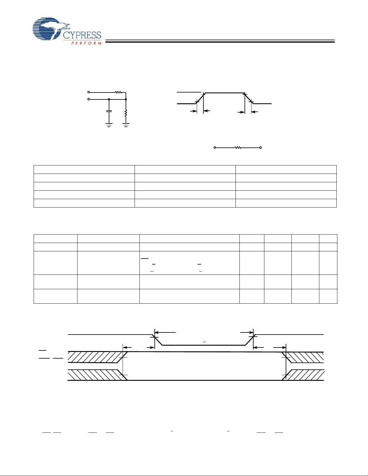
AC Test Loads and Waveforms
CY62167E MoBL
®
V
CC
OUTPUT
30 pF
R1
R2
RISE TIME= 1 V/ns
VCC
GND
10%
ALL INPUT PULSES
90%
90%
10%
INCLUDING
JIG AND
SCOPE
EQUIVALENT TO: THÉVENIN EQUIVALENT
R
OUTPUT
TH
Parameters Values Unit
R1 1800 Ω
R2 990 Ω
R
TH
V
TH
639 Ω
1.77 V
Data Retention Characteristics
Over the Operating Range
Parameter Description Conditions Min Typ
V
DR
I
CCDR
t
CDR
[11]
t
R
[9]
[10]
VCC for Data Retention 2.0 V
Data Retention Current VCC= VDR
CE1 > VCC – 0.2V, CE2 < 0.2V,
V
> VCC – 0.2V or VIN < 0.2V
IN
Chip Deselect to Data
0ns
Retention Time
Operation Recovery
Time
t
RC
FALL TIME= 1 V/ns
V
[4]
Max Unit
12 µA
ns
Data Retention Waveform
[12]
DATA RETENTION MODE
VCC(min)
t
R
CE
BHE
2.0 V
V
CC
or
1
.
BLE
VCC(min)
t
CDR
VDR
>
or
CE
2
Notes
11. Full device operation requires linear V
. BLE is the AND of BHE and BLE. Deselect the chip by either disabling the chip enable signals or by disabling BHE and BLE.
12. BHE
ramp from V
CC
to VCC(min) > 100 µs or stable at VCC(min) > 100 µs.
DR
Document #: 001-15607 Rev. *A Page 4 of 12
[+] Feedback [+] Feedback [+] Feedback
Page 5

CY62167E MoBL
®
Switching Characteristics
Over the Operating Range
Parameter Description
READ CYCLE
t
RC
t
AA
t
OHA
t
ACE
t
DOE
t
LZOE
t
HZOE
t
LZCE
t
HZCE
t
PU
t
PD
t
DBE
t
LZBE
t
HZBE
WRITE CYCLE
t
WC
t
SCE
t
AW
t
HA
t
SA
t
PWE
t
BW
t
SD
t
HD
t
HZWE
t
LZWE
Read Cycle Time 45 ns
Address to Data Valid 45 ns
Data Hold from Address Change 10 ns
CE1 LOW and CE2 HIGH to Data Valid 45 ns
OE LOW to Data Valid 22 ns
OE LOW to LOW-Z
OE HIGH to High-Z
CE1 LOW and CE2 HIGH to Low-Z
CE1 HIGH and CE2 LOW to High-Z
CE1 LOW and CE2 HIGH to Power Up 0 ns
CE1 HIGH and CE2 LOW to Power Down 45 ns
BLE/BHE LOW to Data Valid 45 ns
BLE/BHE LOW to Low-Z
BLE/BHE HIGH to HIGH-Z
[17]
Write Cycle Time 45 ns
CE1 LOW and CE2 HIGH to Write End 35 ns
Address Setup to Write End 35 ns
Address Hold from Write End 0 ns
Address Setup to Write Start 0 ns
WE Pulse Width 35 ns
BLE/BHE LOW to Write End 35 ns
Data Setup to Write End 25 ns
Data Hold from Write End 0 ns
WE LOW to High-Z
WE HIGH to Low-Z
[13, 14]
[15]
[15, 16]
[15]
[15, 16]
[15]
[15, 16]
[15, 16]
[15]
45 ns
Unit
Min Max
5ns
18 ns
10 ns
18 ns
10 ns
18 ns
18 ns
10 ns
Notes
13. Test conditions for all parameters other than tri-state parameters assume signal transition time of 1 V/ns, timing reference levels of V
of 0 to V
14. AC timing parameters are subject to byte enable signals (BHE
15. At any temperature and voltage condition, t
16. t
HZOE
17. The internal write time of the memory is defined by the overlap of WE
a write and any of these signals can terminate a write by going inactive. The data input setup and hold timing should be referenced to the edge of the signal that
terminates the write.
(typ), and output loading of the specified IOL/IOH as shown in “AC Test Loads and Waveforms” on page 4.
, t
CC
HZCE
, t
HZBE
, and t
is less than t
transitions are measured when the outputs enter a high impedance state.
HZWE
HZCE
or BLE) not switching when chip is disabled. See application note AN13842 for further clarification.
, t
LZCE
is less than t
HZBE
, CE1 = VIL, BHE or BLE or both = VIL, and CE2 = VIH. All signals must be active to initiate
LZBE
, t
HZOE
is less than t
LZOE
, and t
HZWE
(typ)/2, input pulse levels
CC
is less than t
LZWE
for any device.
Document #: 001-15607 Rev. *A Page 5 of 12
[+] Feedback [+] Feedback [+] Feedback
Page 6

Switching Waveforms
Figure 1 shows address transition controlled read cycle waveforms.
Figure 1. Read Cycle No. 1
ADDRESS
t
AA
DATA OUT
t
OHA
PREVIOUS DATA VALID DATA VALID
[18, 19]
t
RC
RC
CY62167E MoBL
®
Figure 2 shows OE
ADDRESS
CE
1
CE
2
BHE/BLE
OE
DATA OUT
V
CC
SUPPLY
CURRENT
controlled read cycle waveforms.
Figure 2. Read Cycle No. 2
t
ACE
t
t
LZOE
DBE
t
DOE
50%
t
LZBE
HIGH IMPEDANCE
t
LZCE
t
PU
[19, 20]
t
RC
t
PD
t
HZCE
t
HZBE
t
HZOE
HIGH
DATA VALID
IMPEDANCE
I
CC
50%
I
SB
Notes
18. The device is continuously selected. OE
19. WE
is HIGH for read cycle.
20. Address valid before or similar to CE
, CE1 = VIL, BHE, BLE or both = VIL, and CE2 = VIH.
, BHE, BLE transition LOW and CE2 transition HIGH.
1
Document #: 001-15607 Rev. *A Page 6 of 12
[+] Feedback [+] Feedback [+] Feedback
Page 7

Switching Waveforms (continued)
Figure 3 shows WE
ADDRESS
CE
CE
controlled write cycle waveforms.
1
2
[17, 21, 22]
Figure 3. Write Cycle No. 1
t
WC
t
SCE
CY62167E MoBL
®
WE
BHE/BLE
OE
DATA IO
NOTE 23
t
SA
t
HZOE
t
AW
t
PWE
t
BW
t
SD
t
HA
t
HD
VALID DATA
Notes
21. Data IO is high impedance if OE
22. If CE
23. During this period the IOs are in output state and input signals must not be applied.
goes HIGH and CE2 goes LOW simultaneously with WE = VIH, the output remains in a high impedance state.
1
= VIH.
Document #: 001-15607 Rev. *A Page 7 of 12
[+] Feedback [+] Feedback [+] Feedback
Page 8

Switching Waveforms (continued)
Figure 4 shows CE
ADDRESS
CE
1
CE
2
WE
BHE/BLE
or CE2 controlled write cycle waveforms.
1
[17, 21, 22]
Figure 4. Write Cycle No. 2
t
WC
t
SA
t
AW
t
BW
t
PWE
t
SCE
CY62167E MoBL
t
HA
®
OE
DATA IO
NOTE 23
t
HZOE
Figure 5 shows WE controlled, OE LOW write cycle waveforms.
Figure 5. Write Cycle No. 3
t
WC
ADDRESS
t
SCE
CE
1
CE
2
t
BHE
/BLE
WE
t
SA
BW
t
AW
t
[22]
PWE
t
SD
VALID DATA
t
HD
t
HA
DATA IO
NOTE 23
t
HZWE
t
SD
VAL ID DATA
t
LZWE
t
HD
Document #: 001-15607 Rev. *A Page 8 of 12
[+] Feedback [+] Feedback [+] Feedback
Page 9

Switching Waveforms (continued)
Figure 6 shows BHE
ADDRESS
CE
1
CE
2
/BLE
BHE
WE
/BLE controlled, OE LOW write cycle waveforms.
t
SA
[22]
Figure 6. Write Cycle No. 4
t
WC
t
SCE
t
AW
t
BW
t
PWE
CY62167E MoBL
t
HA
®
DATA IO
NOTE 23
t
SD
VAL ID DATA
t
HD
Document #: 001-15607 Rev. *A Page 9 of 12
[+] Feedback [+] Feedback [+] Feedback
Page 10

Truth Table
CY62167E MoBL
®
CE
CE
1
WE OE BHE BLE Inputs Outputs Mode Power
2
H X X X X X High-Z Deselect/Power Down Standby (I
X L X X X X High-Z Deselect/Power Down Standby (I
X X X X H H High-Z Deselect/Power Down Standby (I
L H H L L L Data Out (IO
L H H L H L Data Out (IO
High-Z (IO
L H H L L H High-Z (IO0–IO7);
Data Out (IO
–IO15) Read Active (ICC)
0
–IO7);
0
–IO15)
8
Read Active (I
Read Active (I
–IO15)
8
L H H H L H High-Z Output Disabled Active (ICC)
L H H H H L High-Z Output Disabled Active (I
L H H H L L High-Z Output Disabled Active (I
LHLXLLData In (IO
LHLXHLData In (IO
High-Z (IO
LHLXLHHigh-Z (IO
Data In (IO
–IO15) Write Active (ICC)
0
–IO7);
0
–IO15)
8
–IO7);
0
–IO15)
8
Write Active (I
Write Active (I
Ordering Information
Speed
(ns) Ordering Code
45 CY62167ELL-45ZXI 51-85183 48-pin TSOP I (Pb-free) Industrial
Package
Diagram
Package Type
Operating
SB
SB
SB
CC
CC
CC
CC
CC
CC
Range
)
)
)
)
)
)
)
)
)
Document #: 001-15607 Rev. *A Page 10 of 12
[+] Feedback [+] Feedback [+] Feedback
Page 11
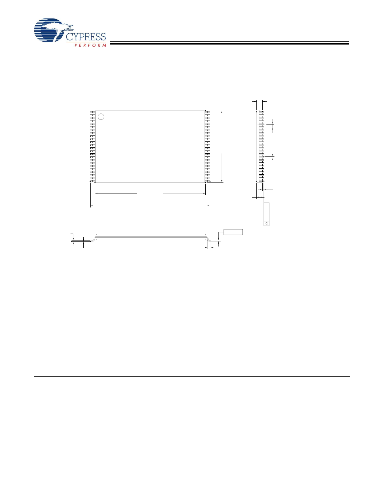
Package Diagram
DIMENSIONS IN INCHES[MM] MIN.
JEDEC # MO-142
CY62167E MoBL
®
Figure 7. 48-Pin TSOP I (12 mm x 18.4 mm x 1.0 mm), 51-85183
MAX.
0.037[0.95]
0.041[1.05]
1
N
0.020[0.50]
TYP.
0.004[0.10]
0.008[0.21]
0°-5°
0.724 [18.40]
0.787[20.00]
0.020[0.50]
0.028[0.70]
0.472[12.00]
0.010[0.25]
GAUGE PLANE
0.047[1.20]
MAX.
SEATING PLANE
0.002[0.05]
0.006[0.15]
0.004[0.10]
0.007[0.17]
0.011[0.27]
51-85183-*A
Document #: 001-15607 Rev. *A Page 11 of 12
© Cypress Semiconductor Corporation, 2007. The information contained herein is subject to change without notice. Cypress Semiconductor Corporation assumes no responsibility for the use
of any circuitry other than circuitry embodied in a Cypress product. Nor does it convey or imply any license under patent or other rights. Cypress products are not warranted nor intended to be
used for medical, life support, life saving, critical control or safety applications, unless pursuant to an express written agreement with Cypress. Furthermore, Cypress does not authorize its
products for use as critical components in life-support systems where a malfunction or failure may reasonably be expected to result in significant injury to the user. The inclusion of Cypress
products in life-support systems application implies that the manufacturer assumes all risk of such use and in doing so indemnifies Cypress against all charges.
MoBL is a registered trademark and More Battery Life is a trademark of Cypress Semiconductor. All product and company names mentioned in this document are the trademarks of their
respective holders.
Any Source Code (software and/or firmware) is owned by Cypress Semiconductor Corporation (Cypress) and is protected by and subject to worldwide patent protection (United States and
foreign), United States copyright laws and international treaty provisions. Cypress hereby grants to licensee a personal, non-exclusive, non-transferable license to copy, use, modify, create
derivative works of, and compile the Cypress Source Code and derivative works for the sole purpose of creating custom software and or firmware in support of licensee product to be used only
in conjunction with a Cypress integrated circuit as specified in the applicable agreement. Any reproduction, modification, translation, compilation, or representation of this Source Code except
as specified above is prohibited without the express written permission of Cypress.
Disclaimer: CYPRESS MAKES NO WARRANTY OF ANY KIND, EXPRESS OR IMPLIED, WITH REGARD TO THIS MATERIAL, INCLUDING, BUT NOT LIMITED TO, THE IMPLIED WARRANTIES OF MERCHANTABILITY AND FITNESS FOR A PARTICULAR PURPOSE. Cypress reserves the right to make changes without further notice to the materials described herein.
Cypress does not assume any liability arising out of the application or use of any product or circuit described herein. Cypress does not authorize its products for use as critical components in
life-support systems where a malfunction or failure may reasonably be expected to result in significant injury to the user. The inclusion of Cypress' product in a life-support systems application
implies that the manufacturer assumes all risk of such use and in doing so indemnifies Cypress against all charges.
Use may be limited by and subject to the applicable Cypress software license agreement.
[+] Feedback [+] Feedback [+] Feedback
Page 12

Document History Page
Document Title: CY62167E MoBL® 16-Mbit (1M x 16 / 2M x 8) Static RAM
Document Number: 001-15607
REV. ECN NO. Issue Date
** 1103145 See ECN VKN New Data Sheet
*A 1138903 See ECN VKN Converted from preliminary to final
Orig. of
Change Description of Change
Changed I
Changed I
Changed I
Added footnote# 8 related to V
Changed I
Added footnote# 14 related to AC timing parameters
spec from 2.8 mA to 4.0 mA for f=1MHz
CC(max)
spec from 22 mA to 25 mA for f=f
CC(typ)
spec from 25 mA to 30 mA for f=f
CC(max)
spec from 10 µA to 12 µA
CCDR
CY62167E MoBL
max
max
IL
®
Document #: 001-15607 Rev. *A Page 12 of 12
[+] Feedback [+] Feedback [+] Feedback
 Loading...