

Page 1
CY62158E MoBL
®
8-Mbit (1M x 8) Static RAM
Features
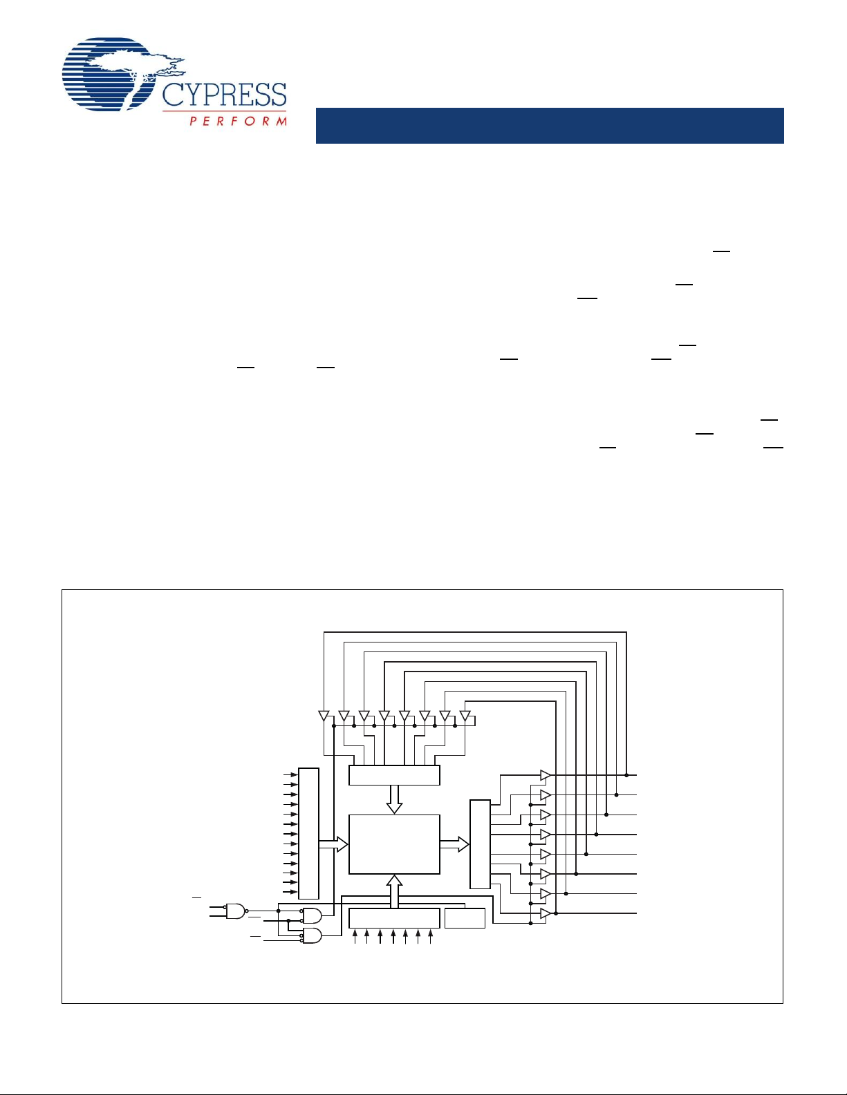
A
0
IO
0
IO
7
IO
1
IO
2
IO
3
IO
4
IO
5
IO
6
A
1
A
2
A
3
A
4
A
5
A
6
A
7
A
8
A
9
SENSE AMPS
POWER
DOWN
WE
OE
A
13
A
14
A15A
16
ROW DECODER
COLUMN DECODER
1024K x 8
ARRAY
DATA IN DRIVERS
A
10
A
11
A
17
CE
1
CE
2
A
12
A18A
19
Logic Block Diagram
■ Very high speed: 45 ns
❐ Wide voltage range: 4.5V – 5.5V
■ Ultra low active power
❐ Typical active current:1.8 mA @ f = 1 MHz
❐ Typical active current: 18 mA @ f = f
■ Ultra low standby power
❐ Typical standby current: 2 μA
❐ Maximum standby current: 8 μA
■ Easy memory expansion with CE
■ Automatic power down when deselected
■ CMOS for optimum speed and power
■ Offered in Pb-free 44-Pin TSOP II package
max
, CE2 and OE features
1
Functional Description
The CY62158E MoBL® is a high performance CMOS static RAM
organized as 1024K words by 8 bits. This device features
advanced circuit design to provide ultra low active current. T his
is ideal for providing More Battery Life™ (MoBL
®
) in portable
applications such as cellular telephones. The device also has an
automatic power down feature that significantly reduces power
consumption. Placing the device into standby mode reduces
power consumption significantly when deselected (CE
CE
LOW).
2
To write to the device, take Chip Enables (CE
HIGH) and Write Enable (WE) input LOW. Data on the eight IO
pins (IO
on the address pins (A
through IO7) is then written into the location specified
0
through A19).
0
To read from the device, take Chip Enables (CE
HIGH) and OE LOW while forcing the WE HIGH. Under these
1
1
HIGH or
1
LOW and CE
LOW and CE
conditions, the contents of the memory location specified by the
address pins appear on the IO pins.
The eight input and output pins (IO
a high impedance state when the device is deselected (CE
through IO7) are placed in
0
HIGH or CE2 LOW), the outputs are disabled (OE HIGH), or a
write operation is in progress (CE
LOW). See the Truth Table on page 8 for a complete description
LOW and CE2 HIGH and WE
1
of read and write modes.
For best practice recommendations, refer to the Cypress
application note AN1064, SRAM System Guidelines.
2
2
1
Cypress Semiconductor Corporation • 198 Champion Court • San Jose, CA 95134-1709 • 408-943-2600
Document #: 38-05684 Rev. *D Revised June 16, 2008
[+] Feedback
Page 2
CY62158E MoBL
®
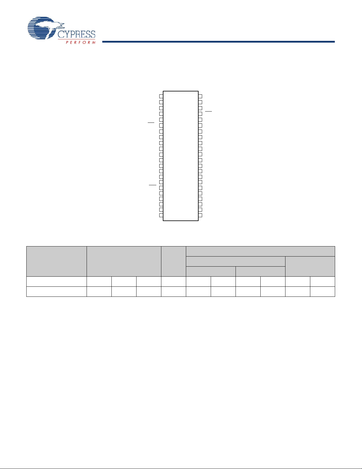
Pin Configuration
1
2
3
4
5
6
7
8
9
11
14
31
32
36
35
34
33
37
40
39
38
12
13
41
44
43
42
16
15
29
30
A
5
18
17
20
19
23
28
25
24
22
21
27
26
A
6
A
7
A
4
A
3
A
2
A
1
A
0
A
17
A
18
A
10
A
11
A
12
A
13
A
15
A
16
A
14
OE
CE
2
A
8
CE
1
WE
NC
NC
IO
0
IO
1
IO
2
IO
3
NC
NC
NC
NC
IO
4
IO
5
IO
6
IO
7
NC
NC
V
CC
V
CC
V
SS
V
SS
A
9
10
A
19
Notes
1. NC pins are not connected on the die.
2. Typical values are included for reference only and are not guaranteed or tested. Typical values are measured at V
CC
= V
CC(typ)
, TA = 25°C.
Product Portfolio
Figure 1. 44-Pin TSOP II (Top View)
[1]
Product VCC Range (V)
Speed
(ns)
f = 1 MHz f = f
Min Typ
[2]
Max Typ
[2]
CY62158ELL 4.5 5.0 5.5 45 1.8 3 18 25 2 8
Document #: 38-05684 Rev. *D Page 2 of 10
Operating I
Max Typ
Power Dissipation
(mA)
CC
max
[2]
Max Typ
Standby I
[2]
SB2
(μA)
Max
[+] Feedback
Page 3
CY62158E MoBL
®
Maximum Ratings
Notes
3. V
IL
(min) = –2.0V for pulse durations less than 20 ns.
4. V
IH
(max) = VCC + 0.75V for pulse durations less than 20 ns.
5. Full Device AC operation assumes a 100 μs ramp time from 0 to V
CC
(min) and 200 μs wait time after VCC stabilization.
6. Only chip enables (CE
1
and CE2), must be tied to CMOS levels to meet the I
SB2
/ I
CCDR
spec. Other inputs can be left floating.
Exceeding the maximum ratings may impair the useful life of the
device. These user guidelines are not tested.
Storage Temperature.................................. –65°C to +150°C
Ambient Temperature with
Power Applied ............................................–55°C to +125°C
Supply Voltage to Ground Potential–0.5V to V
DC Voltage Applied to Outputs
in High-Z State
[3, 4]
........................–0.5V to V
CC(max)
CC(max)
+ 0.5V
+ 0.5V
DC Input Voltage
Output Current into Outputs (LOW).............................20 mA
Static Discharge Voltage............................................>2001V
(MIL-STD-883, Method 3015)
Latch up Current......................................................>200 mA
Operating Range
CY62158ELL Industrial –40°C to +85°C 4.5V – 5.5V
Electrical Characteristics
Over the Operating Range
Parameter Description Test Conditions
V
V
V
V
I
IX
I
OZ
I
CC
I
SB1
I
SB2
OH
OL
IH
IIL
[6]
Output HIGH Voltage IOH = –1 mA 2.4 V
Output LOW Voltage IOL = 2.1 mA 0.4 V
Input HIGH Voltage V
Input LOW Voltage V
Input Leakage Current GND < VI < V
= 4.5V to 5.5V 2.2 V
CC
= 4.5V to 5.5V –0.5 0.8 V
CC
CC
Output Leakage Current GND < VO < VCC, Output Disabled –1 +1 μA
VCC Operating Supply
Current
Automatic CE Power down
Current — CMOS Inputs
Automatic CE Power-down
Current — CMOS Inputs
f = f
f = 1 MHz 1.8 3 mA
MAX
= 1/t
RC
VCC = V
I
OUT
CMOS levels
CE1 > VCC− 0.2V, CE2 < 0.2V
V
> VCC – 0.2V, VIN < 0.2V)
IN
f = f
f = 0 (OE
(Address and Data Only),
MAX
, and WE), V
CC
= V
CE1 > VCC – 0.2V or CE2 < 0.2V,
> VCC – 0.2V or VIN < 0.2V,
V
IN
f = 0, V
CC
= V
CCmax
[3, 4]
.....................–0.5V to V
Device Range
CCmax
= 0 mA
CCmax
+ 0.5V
CC(max)
Ambient
Temperature
[5]
V
CC
-45
[2]
Max
CC
UnitMin Typ
+ 0.5V V
–1 +1 μA
18 25 mA
28μA
28μA
Capacitance
Tested initially and after any design or process changes that may affect these parameters.
Parameter Description Test Conditions Max Unit
C
IN
C
OUT
Input Capacitance TA = 25°C, f = 1 MHz,
Output Capacitance 10 pF
Thermal Resistance
Tested initially and after any design or process changes that may affect these parameters.
Parameter Description Test Conditions TSOP II Unit
Θ
Θ
Document #: 38-05684 Rev. *D Page 3 of 10
Thermal Resistance
JA
(Junction to Ambient)
Thermal Resistance
JC
(Junction to Case)
= V
V
CC
CC(typ)
Still Air, soldered on a 3 × 4.5 inch,
two-layer printed circuit board
10 pF
75.13 °C/W
8.95 °C/W
[+] Feedback
Page 4

CY62158E MoBL
®
Figure 2. AC Test Loads and Waveforms
3V
V
CC
OUTPUT
R2
100 pF
INCLUDING
JIG AND
SCOPE
GND
90%
10%
90%
10%
Rise Time = 1 V/ns
Fall Time = 1 V/ns
OUTPUT V
Equivalent to: THÉVENIN EQUIVALENT
ALL INPUT PULSES
R
TH
R1
Notes
7. Teste d initially and after any design or process changes that may affect these parameters.
8. Full device operation requires linear V
CC
ramp from V
DR
to VCC(min) > 100 μs or stable at VCC(min) > 100 μs.
VCC(min)
VCC(min)
t
CDR
VDR
>
2.0 V
DATA RETENTION MODE
t
R
CE
1
V
CC
CE
2
or
Parameters 5.0V Unit
R1 1838 Ω
R2 994 Ω
R
TH
V
TH
645 Ω
1.75 V
Data Retention Characteristics
Over the Operating Range
Parameter Description Conditions Min Typ
V
DR
I
CCDR
t
CDR
[8]
t
R
[7]
VCC for Data Retention 2 V
[6]
Data Retention Current VCC = V
DR
CE1 > VCC − 0.2V, CE2 < 0.2V,
V
> VCC − 0.2V or VIN < 0.2V
IN
Chip Deselect to Data
0ns
Retention Time
Operation Recovery Time t
RC
[2]
Max Unit
8 μA
ns
Figure 3. Data Retention Waveform
Document #: 38-05684 Rev. *D Page 4 of 10
[+] Feedback
Page 5

CY62158E MoBL
®
Switching Characteristics
Notes
9. Test cond itions for all p arameters other than tri-st ate p arameters assume signal tr ansition time of 3 ns or less (1V/ns), timing reference levels of V
CC(typ)
/2, input pulse
levels of 0 to V
CC(typ)
, and output loading of the specified IOL/IOH as shown in “AC Test Loads and Waveforms” on page 4.
10.At any given temperature and voltage condition, t
HZCE
is less than t
LZCE
, t
HZOE
is less than t
LZOE
, and t
HZWE
is less than t
LZWE
for any given device.
11. t
HZOE
, t
HZCE
, and t
HZWE
transitions are measured when the outputs enter a high impedance state.
12.The internal write time of the memory is defined by the overlap of WE
, CE1 = VIL, and CE2 = VIH. All signals must be ACTIVE to initiate a write and any of these signals
can terminate a write by going INACTIVE. The data input setup and hold timing should be referenced to the edge of the signal that terminates the write.
Over the Operating Range
Parameter Description
Read Cycle
t
RC
t
AA
t
OHA
t
ACE
t
DOE
t
LZOE
t
HZOE
t
LZCE
t
HZCE
t
PU
t
PD
Write Cycle
t
WC
t
SCE
t
AW
t
HA
t
SA
t
PWE
t
SD
t
HD
t
HZWE
t
LZWE
Read Cycle Time 45 ns
Address to Data Valid 45 ns
Data Hold from Address Change 10 ns
CE1 LOW and CE2 HIGH to Data Valid 45 ns
OE LOW to Data Valid 22 ns
OE LOW to Low Z
OE HIGH to High Z
CE1 LOW and CE2 HIGH to Low Z
CE1 HIGH or CE2 LOW to High Z
CE1 LOW and CE2 HIGH to Power Up 0 ns
CE1 HIGH or CE2 LOW to Power Down 45 ns
[12]
Write Cycle Time 45 ns
CE1 LOW and CE2 HIGH to Write End 35 ns
Address Setup to Write End 35 ns
Address Hold from Write End 0 ns
Address Setup to Write Start 0 ns
WE Pulse Width 35 ns
Data Setup to Write End 25 ns
Data Hold from Write End 0 ns
WE LOW to High Z
WE HIGH to Low Z
[9]
[10]
[10, 1 1]
[10]
[10, 11]
[10, 11]
[10]
45 ns
Min Max
Unit
5ns
18 ns
10 ns
18 ns
18 ns
10 ns
Document #: 38-05684 Rev. *D Page 5 of 10
[+] Feedback
Page 6

CY62158E MoBL
®
Switching Waveforms
ADDRESS
DATA OUT
PREVIOUS DATA VALID
DATA VALID
t
RC
t
AA
t
OHA
50%
50%
DATA VALID
t
RC
t
ACE
t
DOE
t
LZOE
t
LZCE
t
PU
HIGH IMPEDANCE
t
HZOE
t
HZCE
t
PD
HIGH
I
CC
I
SB
IMPEDANCE
OE
CE
1
ADDRESS
CE
2
DATA OUT
SUPPLY
CURRENT
V
CC
Notes
13.Device is continuously selected. OE
, CE1 = VIL, CE2 = VIH.
14.WE
is HIGH for read cycle.
15.Address valid before or similar to CE
1
transition LOW and CE2 transition HIGH.
Figure 4 shows address transition controlled read cycle waveforms.
Figure 4. Read Cycle No. 1
[13, 14]
Figure 5 shows OE
controlled read cycle waveforms.
[14, 15]
Figure 5. Read Cycle No. 2
Document #: 38-05684 Rev. *D Page 6 of 10
[+] Feedback
Page 7

CY62158E MoBL
®
Switching Waveforms (continued)
t
HD
t
SD
t
PWE
t
SA
t
HA
t
AW
t
SCE
t
WC
t
HZOE
VALID DATA
NOTE 18
CE
1
ADDRESS
CE
2
WE
DATA IO
OE
t
WC
VALID DATA
t
AW
t
SA
t
PWE
t
HA
t
HD
t
SD
t
SCE
CE
1
ADDRESS
CE
2
WE
DATA IO
OE
Notes
16.Data IO is high impedance if OE
= VIH.
17.If CE
1
goes HIGH or CE2 goes LOW simultaneously with WE HIGH, the output remains in high impedance state.
18.During this period, the IOs are in output state. Do not apply input signals.
Figure 6 shows WE controlled write cycle waveforms.
[12, 16, 17]
Figure 6. Write Cycle No. 1
Figure 7 shows CE1 or CE2 controlled write cycle waveforms.
[12, 16, 17]
Figure 7. Write Cycle No. 2
Document #: 38-05684 Rev. *D Page 7 of 10
[+] Feedback
Page 8

CY62158E MoBL
®
Switching Waveforms (continued)
VALID DATA
t
HD
t
SD
t
LZWE
t
PWE
t
SA
t
HA
t
AW
t
SCE
t
WC
t
HZWE
NOTE 18
CE
1
ADDRESS
CE
2
WE
DATA IO
Figure 8 shows WE controlled, OE LOW write cycle waveforms.
Figure 8. Write Cycle No. 3
[17]
Truth Table
CE
1
H X X X High Z Deselect/Power Down Standby (ISB)
X L X X High Z Deselect/Power Down Standby (ISB)
L H H L Data Out Read Active (ICC)
L H H H High Z Output Disabled Active (ICC)
L H L X Data in Write Active (ICC)
CE
2
WE OE Inputs/Outputs Mode Power
Ordering Information
Speed
(ns) Ordering Code
45 CY62158ELL-45ZSXI 51-85087 44-Pin TSOP II (Pb-free) Industrial
Package
Diagram
Package Type
Operating
Range
Document #: 38-05684 Rev. *D Page 8 of 10
[+] Feedback
Page 9

CY62158E MoBL
®
Package Diagrams
51-85087-*A
Figure 9. 44-Pin TSOP II, 51-85087
Document #: 38-05684 Rev. *D Page 9 of 10
[+] Feedback
Page 10

CY62158E MoBL
®
Document History Page
Document Title: CY62158E MoBL® 8-Mbit (1M x 8) Static RAM
Document Number: 38-05684
REV. ECN NO. Issue Date
** 270350 See ECN PCI New Data Sheet
*A 291271 See ECN SYT Converted from Advance Information to Preliminary
*B 1462592 See ECN VKN/AESA Converted from preliminary to final
*C 2428708 See ECN VKN/PYRS Corrected typo in the Ordering Information table
*D 2516494 See ECN PYRS Corrected ECN number
Orig. of
Change Description of Change
Changed input pulse level from VCC to 3V in the AC T est Loads and W aveforms
Modified footnote #9 to include timing reference level of 1.5V and input pulse
level of 3V
Removed 35 ns speed bin
Removed “L” parts
Removed 48-Ball VFBGA package
Changed I
Changed I
Changed I
Changed I
Changed I
Changed I
Changed t
Changed t
Changed t
Changed t
Changed t
Changed t
Added footnote# 6 related to I
spec from 2.3 mA to 3 mA at f=1 MHz
CC(max)
spec from 16 mA to 18 mA at f=f
CC(typ)
spec from 28 mA to 25 mA at f=f
CC(max)
and I
SB1(typ)
SB1(max)
CCDR(max)
LZOE
LZCE
HZCE
PWE
SD
LZWE
and I
spec from 4.5 μA to 8 μA
spec from 3 ns to 5 ns
spec from 6 ns to 10 ns
spec from 22 ns to 18 ns
spec from 30 ns to 35 ns
spec from 22 ns to 25 ns
spec from 6 ns to 10 ns
Updated Ordering information table
spec from 0.9 μA to 2 μA
SB2(typ)
SB2(max)
spec from 4.5 μA to 8 μA
and I
SB2
CCDR
MAX
MAX
© Cypress Semiconductor Corporation, 2008. The information contained herein is subject to change without notice. Cypress Semiconductor Corporation assumes no responsibility for the use of any
circuitry other than circuitry embodied in a Cypress product. Nor does it convey or imply any license under patent or other rights. Cypress products are not warranted nor intend ed to be used for medical ,
life support, life saving, critical control or safety applications, unless pursuant to an express written agreement with Cypress. Furthermore, Cypress does not authorize its products for use as critical
components in life-support systems where a malfunction or failure may reasonably be expected to result in significant injury to the user. The inclusion of Cypress products in life-support systems
application implies that the manufacturer assumes all risk of such use and in doing so indemnifies Cypress against all charges.
Any Source Code (software and/or firmware) is owned by Cypress Semiconductor Corporation (Cypress) and is protected by and subject to worldwide patent protection (United States and foreign),
United States copyright laws and international treaty provisions. Cypress hereby gr ant s to l icense e a pers onal, no n-exclu sive , non-tr ansfer able license to copy, use, modify, create derivative works of,
and compile the Cypress Source Code and derivative works for the sole purpose of creating custom software and or firmware in support of licensee product to be used only in conjuncti on with a Cypress
integrated circuit as specified in the ap plicable agreem ent. Any reprod uction, modificatio n, translation, co mpilation, or repr esentation of this Source Co de except as speci fied above is pro hibited with out
the express written permission of Cypress.
Disclaimer: CYPRESS MAKES NO WARRANTY OF ANY KIND, EXPRESS OR IMPLIED, WITH REGARD TO THIS MATERIAL, INCLUDING, BUT NOT LIMITED TO, THE IMPLIED WARRANTIES
OF MERCHANTABILITY AND FITNESS FOR A PARTICULAR PURPOSE. Cypress reserves the right to make changes without further notice to the materials described herein. Cyp ress does not
assume any liability arising out of the applic ation or use o f any pr oduct or circ uit de scribed herein . Cypr ess does n ot author ize its p roducts fo r use as critical compon ents in life-su pport systems whe re
a malfunction or failure may reason ably be expected to result in significant injury to the user. The inclusion of Cypress’ product in a life-support systems application implies that the manufacturer
assumes all risk of such use and in doing so indemnifies Cypress against all charges.
Use may be limited by and subject to the applicable Cypress software license agreement.
Document #: 38-05684 Rev. *D Revised June 16, 2008 Page 10 of 10
All products and company names mentioned in this document may be the trademarks of their respective holders.
[+] Feedback
 Loading...