

Page 1
CY62148BN MoBL
®
4-Mbit (512K x 8) Static RAM
Features
• High Speed
—70 ns
• 4.5V–5.5V operation
• Low active power
— Typical active current: 2.5 mA @ f = 1 MHz
— Typical active current:12.5 mA @ f = f
max
(70 ns)
• Low standby curr en t
• Automatic power-down when deselected
• TTL-compatible inputs and outputs
• Easy memory expansion with CE
and OE features
• CMOS for optimum speed/power
• Available in standard lead-free and non-lead-free
32-lead (450-mil) SOIC, 32-lead TSOP II and 32-lead
Reverse TSOP II packages
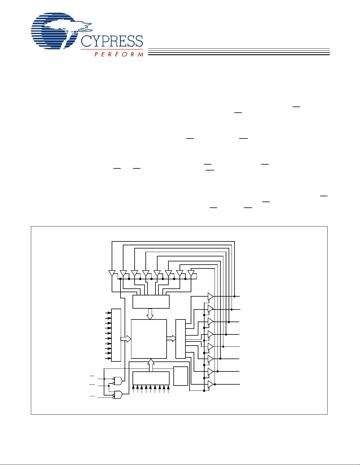
Logic Block Diagram
Functional Description
The CY62148BN is a high-performance CMOS static RAM
organized as 512K words by 8 bits. Easy memory expansion
is provided by an active LOW Chip Enable (CE), an active
LOW Output Enable (OE
has an automatic power-down feature that reduces power
consumption by more than 99% when deselected.
Writing to the device is accomplished by taking Chip Enable
(CE
) and Write Enable (WE) inputs LOW. Data on the eight I/O
pins (I/O
specified on the address pins (A
through I/O7) is then written into the location
0
Reading from the device is accomplished by taking Chip
Enable (CE
Enable (WE
) and Output Enable (OE) LOW while forcing Write
) HIGH for read. Under these conditions, the
contents of the memory location specified by the address pins
will appear on the I/O pins.
The eight input/output pins (I/O0 through I/O7) are placed in a
high-impedance state when the device is deselected (CE
HIGH), the outputs are disabled (OE HIGH), or during a write
operation (CE
LOW, and WE LOW).
), and three-state drivers. This device
through A18).
0
I/O
I/O
I/O
I/O
I/O
I/O
I/O
I/O
0
1
2
3
4
5
6
7
WE
OE
INPUT BUFFER
A
0
A
1
A
4
A
5
A
6
A
7
A
12
A
14
A
16
A
17
ROW DECODER
3
2
A
A
512 xK8
ARRAY
COLUMN
DECODER
15
18
13
A
A
ACEA
SENSE AMPS
POWER
DOWN
8
9
11
10
A
A
A
Cypress Semiconductor Corporation • 198 Champion Court • San Jose, CA 95134-1709 • 408-943-2600
Document #: 001-06517 Rev. *A Revised August 2, 2006
[+] Feedback
Page 2
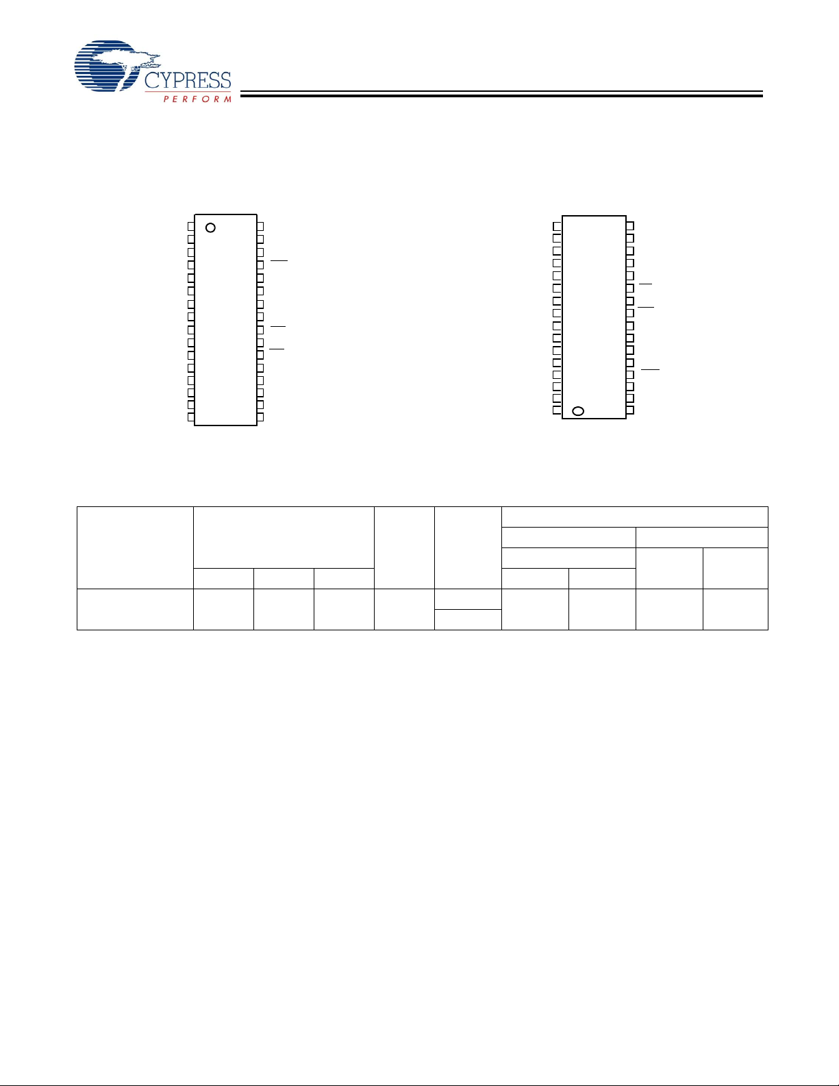
Pin Configuration
CY62148BN MoBL
®
A
A
A
A
I/O
I/O
I/O
GND
17
16
14
12
A
7
A
6
A
5
A
4
A
3
A
2
A
1
A
0
0
1
2
Top View
SOIC
TSOP II
1
2
3
4
5
6
7
8
9
10
11
12
13
14
15
16
32
31
30
29
28
27
26
25
24
23
22
21
20
19
18
17
V
A
A
WE
A
A
A
A
OE
A
CE
I/O
I/O
I/O
I/O
I/O
I/O
CC
18
9
10
GND
15
13
8
11
7
6
5
4
3
A
A
A
I/O
I/O
I/O
A
2
1
0
A
0
A
1
A
2
A
3
A
4
A
5
A
6
A
7
12
14
16
17
Top View
Reverse
TSOP II
16
15
14
13
12
11
10
9
8
7
6
5
4
3
2
1
17
18
19
20
21
22
23
24
25
26
27
28
29
30
31
32
I/O
I/O
I/O
I/O
I/O
CE
A
OE
A
A
A
A
WE
A
A
V
3
4
5
6
7
10
11
9
8
13
18
15
cc
Product Portfolio
Power Dissipation
Product
VCC Range
Speed Temp.
Operating, I
f = f
[1]
CC
max
Max.
CY62148BNLL 4.5 V 5.0V 5.5V 70 ns Com’l 12.5 mA 20 mA 4 µA 20 µA
Ind’l
Note:
1. Typical values are measured at V
= 5V, TA = 25°C, and are included for reference only and are not tested or guaranteed.
CC
Standby (I
[1]
Typ.
SB2
Max.Min. Typ. Max. Typ.
)
Document #: 001-06517 Rev. *A Page 2 of 10
[+] Feedback
Page 3
CY62148BN MoBL
®
Maximum Ratings
(Above which the useful life may be impaired. For user guidelines, not tested.)
Storage Temperature .................................–65°C to +150°C
Ambient Temperature with
Power Applied.............................................–55°C to +125°C
Supply Voltage on V
DC Voltage Applied to Outputs
in High Z State
[2]
DC Input Voltage
to Relative GND........–0.5V to +7.0V
CC
.....................................–0.5V to VCC +0.5V
[2]
..................................–0.5V to VCC +0.5V
Current into Outputs (LOW).........................................20 mA
Static Discharge Voltage............. ... ... ............................2001V
(per MIL-STD-883, Method 3015)
Latch-Up Current.....................................................>200 mA
Operating Range
Commercial 0°C to +70°C 4.5V–5.5V
Industrial –40°C to +85°C
Electrical Characteristics Over the Operating Range
Parameter Description Test Conditions
V
V
V
V
I
IX
I
OZ
I
CC
I
SB1
I
SB2
OH
OL
IH
IL
Output HIGH Voltage VCC = Min., IOH = – 1 mA 2.4 V
Output LOW Voltage VCC = Min., IOL = 2.1 mA 0.4 V
Input HIGH Voltage 2.2 VCC+0.3 V
Input LOW Voltage –0.3 0.8 V
Input Leakage Current GND ≤ VI ≤ V
CC
Output Leakage Current GND ≤ VI ≤ VCC, Output Disabled –1 +1 µA
VCC Operating
Supply Current
Automatic CE
Power-Down Current
—T TL Inputs
Automatic CE
Power-Down Current
—C MOS Inputs
f = f
f = 1 MHz 2.5 mA
Max. VCC,CE ≤ V
VIN ≤ VIH or VIN ≤ VIL,
f = f
Max. VCC,
CE
V
or V
= 1/t
MAX
MAX
≤ VCC – 0.3V,
≤ VCC – 0.3V,
IN
≤ 0.3V, f =0
IN
RC
IH
Com’l/Ind’l
I
V
Com’l/
Ind’l
Com’l/
Ind’l
OUT
CC
Range
=0 mA
= Max.,
Ambient
Temperature
[3]
V
CC
CY62148BN-70
[1]
Max.
UnitMin. Typ.
–1 +1 µA
12.5 20 mA
1.5 mA
4 20 µA
Capacitance
[4]
Parameter Description Test Conditions Max. Unit
C
C
IN
OUT
Input Capacitance TA = 25°C, f = 1 MHz,
= 5.0V
V
Output Capacitance 8 pF
CC
6 pF
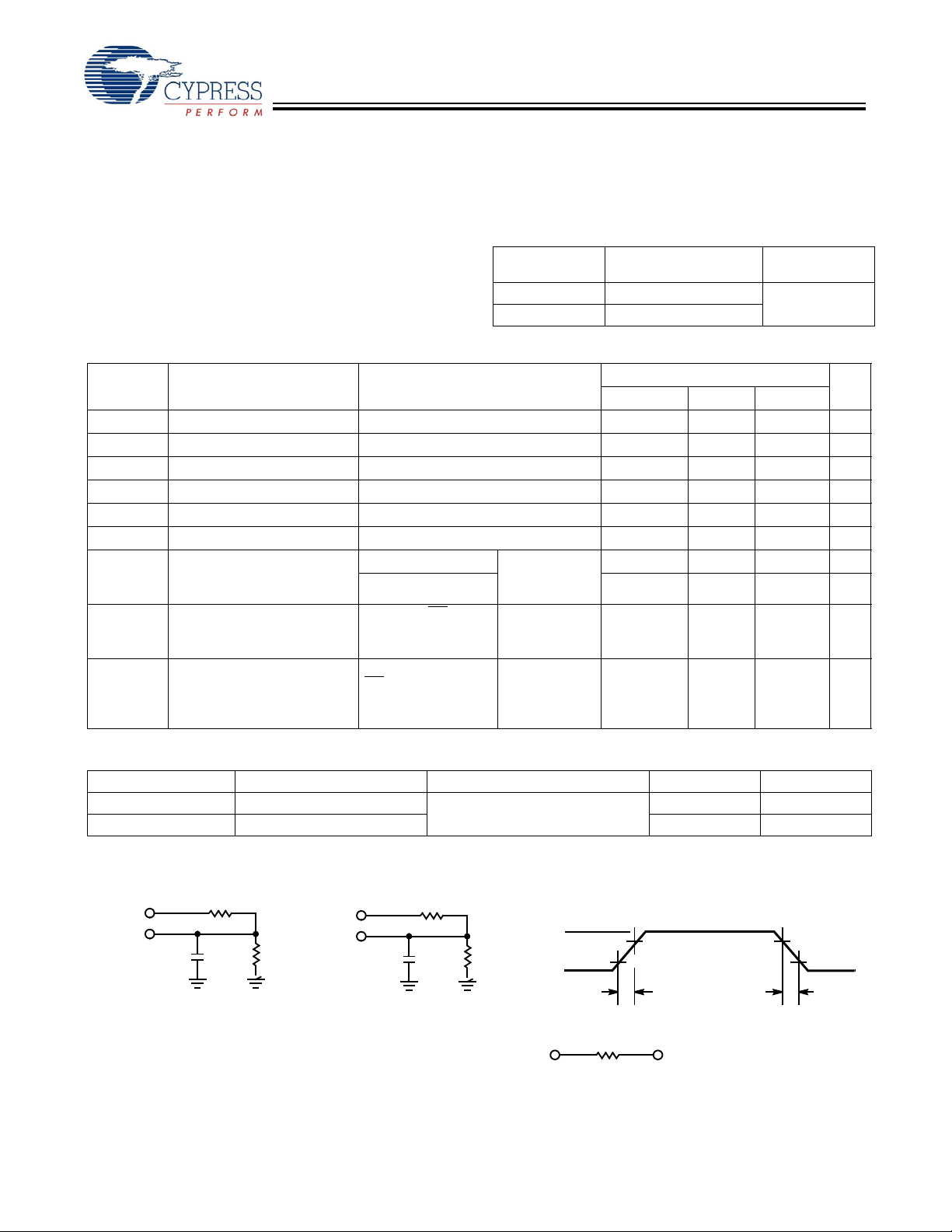
AC Test Loads and Waveforms
5 pF
R1 1800Ω
(b)
ALL INPUT PULSES
3.0V
R2
990Ω
Equivalent to: THEVENIN EQUIVALENT
GND
OUTPUT
≤ 3 ns ≤ 3ns
639Ω
90%
10%
1.77V
90%
10%
R1 1800Ω
5V
OUTPUT
100 pF
INCLUDING
JIG AND
SCOPE
Notes:
(min.) = –2.0V for pulse durations of less than 20 ns.
2. V
IL
is the “Instant On” case temperature
3. T
A
4. Tested initially and after any design or process ch anges that may affect these parameters.
(a)
R2
990Ω
5V
OUTPUT
INCLUDING
JIG AND
SCOPE
Document #: 001-06517 Rev. *A Page 3 of 10
[+] Feedback
Page 4

CY62148BN MoBL
®
Switching Characteristics
[5]
Over the Operating Range
Parameter Description
READ CYCLE
t
RC
t
AA
t
OHA
t
ACE
t
DOE
t
LZOE
t
HZOE
t
LZCE
t
HZCE
t
PU
t
PD
WRITE CYCLE
t
WC
t
SCE
t
AW
t
HA
t
SA
t
PWE
t
SD
t
HD
t
LZWE
t
HZWE
[8]
Read Cycle Time 70 ns
Address to Data Valid 70 ns
Data Hold from Address Change 10 ns
CE LOW to Data Va lid 70 ns
OE LOW to Data V alid 35 ns
OE LOW to Low Z
OE HIGH to High Z
CE LOW to Low Z
CE HIGH to High Z
CE LOW to Power-Up 0 ns
CE HIGH to Power-Down 70 ns
Write Cycle Time 70 ns
CE LOW to Write End 60 ns
Address Set-Up to Write End 60 ns
Address Hold from Write End 0 ns
Address Set-Up to Write Start 0 ns
WE Pulse Width 55 ns
Data Set-Up to Write End 30 ns
Data Hold from Write End 0 ns
WE HIGH to Low Z
WE LOW to High Z
[6]
[6]
[6, 7]
[6, 7]
[6]
[6, 7]
62148BNLL-70
UnitMin. Max.
5 ns
25 ns
10 ns
25 ns
5 ns
25 ns
Notes:
5. Test conditions assume signal transition time of 5 ns or less, timi ng re fe rence l evels of 1. 5V, input pulse levels of 0 to 3.0V, and output loading of the specified
6. At any given temperature and voltage condition, t
7. t
8. The internal write time of the memory is defined by the overlap of CE
and 100-pF load capacitance.
I
OL/IOH
, t
HZCE
, and t
HZOE
any of these signals can terminate the write. The input dat a set-up and hold timing should be referenced t o the leading edge of the signal that terminat es the write.
are specified with a load capacitance of 5 pF as in part (b) of AC Test Loads. Transition is measured ±500 mV from steady-state volt age.
HZWE
is less than t
HZCE
, t
LZCE
is less than t
HZOE
LOW, and WE LOW. CE and WE must be LOW to initiate a write, and the transition of
LZOE
, and t
is less than t
HZWE
for any given device.
LZWE
Document #: 001-06517 Rev. *A Page 4 of 10
[+] Feedback
Page 5

Data Retention Characteristics (Over the Operating Range)
Parameter Description Conditions Min. Typ.
V
DR
I
CCDR
[4]
t
CDR
[9]
t
R
Data Retention Waveform
V
CC
CE
Switching Waveforms
Read Cycle No.1
VCC for Data Retention 2.0 V
Data Retention Current Com’l LL No input may exceed
V
+ 0.3V
Ind’l LL 20 µA
Chip Deselect to Data Retention Time 0 ns
Operation Recovery Time t
t
CDR
[10, 11]
CC
V
= VDR = 3.0V
CC
CE
> VCC – 0.3V
> VCC – 0.3V or
V
IN
V
< 0.3V
IN
DATA RETENTION MODE
VDR> 2V
RC
CY62148BN MoBL
[1]
Max. Unit
20 µA
ns
3.0V3.0V
t
R
®
ADDRESS
DATA OUT
PREVIOUS DATA VALID DATA VALID
Read Cycle No. 2 (OE Controlled)
ADDRESS
CE
OE
DATA OUT
V
CC
SUPPLY
CURRENT
HIGH IMPEDANCE
t
LZCE
t
PU
[11, 12]
t
ACE
t
LZOE
t
OHA
50%
t
DOE
t
RC
t
AA
t
RC
t
HZOE
t
DATA VALID
HZCE
t
PD
HIGH
IMPEDANCE
50%
I
SB
Notes:
9. Full Device operation requires linear V
10.Device is continuously selected. OE
is HIGH for read cycle.
11. WE
12.Address valid prior to or coincident with CE
ramp from V
CC
, CE = VIL.
transition LOW.
DR
to V
> 100 ms or stable at V
CC(min)
cc(min)
> 100 ms.
Document #: 001-06517 Rev. *A Page 5 of 10
[+] Feedback
Page 6

Switching Waveforms (continued)
Write Cycle No. 1 (CE Controlled)
ADDRESS
CE
[13]
CY62148BN MoBL
t
WC
t
SCE
t
SA
®
t
AW
WE
DATA I/O
Write Cycle No. 2 (WE Controlled, OE HIGH During Write)
ADDRESS
t
SCE
CE
t
HZCE
t
AW
t
SA
WE
OE
[13, 14]
t
WC
t
PWE
t
SD
DATA VALID
t
PWE
t
HA
t
HD
t
HA
t
SD
DATA I/O
Notes:
goes HIGH simultaneously with WE going HIGH, the output remains in a high-impedance state.
13.If CE
14.Data I/O is high-impedance if OE
15.During this period the I/Os are in the output state and input signals should not be applied.
NOTE
15
= VIH.
t
HZOE
DATAINVALID
t
HD
Document #: 001-06517 Rev. *A Page 6 of 10
[+] Feedback
Page 7

Switching Waveforms (continued)
Write Cycle No.3 (WE Controlled, OE LOW)
ADDRESS
CE
t
HZCE
[13, 14]
t
SCE
t
WC
CY62148BN MoBL
®
t
HA
t
LZWE
t
HD
WE
DATAI/O
NOTE 15
t
AW
t
SA
t
HZWE
t
PWE
t
SD
DATA VALID
Truth Table
CE OE WE I/O0–I/O
7
H X X High Z Power-Down Standby (ISB)
L L H Data Out Read Active (ICC)
L X L Data In Write Active (ICC)
L H H High Z Selected, Outputs Disabled Active (ICC)
Mode Power
Ordering Information
Speed
(ns) Ordering Code
70 CY62148BNLL-70SC 51-85081 32-lead (450-Mil) Molded SOIC Commercial
CY62148BNLL-70SXC 51-85081 32-lead (450-Mil) Molded SOIC (Pb-Free)
CY62148BNLL-70ZC 51-85095 32-lead TSOP II
CY62148BNLL-70ZXC 51-85095 32-lead TSOP II (Pb-Free)
CY62148BNLL-70ZRC 51-85138 32-lead RTSOP II
CY62148BNLL-70SI 51-85081 32-lead (450-Mil) Molded SOIC Industrial
CY62148BNLL-70SXI 51-85081 32-lead (450-Mil) Molded SOIC (Pb-Free)
CY62148BNLL-70ZI 51-85095 32-lead TSOP II
CY62148BNLL-70ZXI 51-85095 32-lead TSOP II (Pb-Free)
CY62148BNLL-70ZRI 51-85138 32-lead RTSOP II
Please contact your local Cypress sales representative for availability of these parts
Package
Diagram Package Type
Operating
Range
Document #: 001-06517 Rev. *A Page 7 of 10
[+] Feedback
Page 8

Package Diagrams
32 LD (450 Mil) SOIC
32-lead (450-Mil) Molde d SOIC (51-85081)
116
0.546[13.868]
0.566[14.376]
CY62148BN MoBL
®
0.101[2.565]
0.111[2.819]
17 32
0.793[20.142]
0.817[20.751]
0.050[1.270]
BSC.
0.014[0.355]
0.020[0.508]
32-Lead
Thin Small Outline Package Type II (51-85095)
0.004[0.102]
SEATING PLANE
MIN.
0.440[11.176]
0.450[11.430]
0.118[2.997]
MAX.
0.004[0.102]
DIMENSIONS IN INCHES[MM]
PACKAGE WEIGHT 1.42gms
0.023[0.584]
0.039[0.990]
PART #
0.006[0.152]
0.012[0.304]
S32.45 STANDARD PKG.
SZ32.45 LEAD FREE PKG.
0.047[1.193]
0.063[1.600]
MIN.
MAX.
51-85081-*B
51-85095 **
Document #: 001-06517 Rev. *A Page 8 of 10
[+] Feedback
Page 9

Package Diagrams (continued)
32-lead Reverse Thin Small Outline Package Type II (51-85138)
CY62148BN MoBL
®
51-85138-**
More Battery Life is a trademark, and MoBL is a registered trademark, of Cypress Semiconductor. All products and company
names mentioned in this document may be the trademarks of their respective holders.
Document #: 001-06517 Rev. *A Page 9 of 10
© Cypress Semiconductor Corporation, 2006. The information contained herein is subject to ch an ge without notice. Cypress Semiconductor Corporation assumes no resp onsibility f or the u se
of any circuitry other than circuitry embodied in a Cypress product. Nor does it convey or imply any license under patent or other rights. Cypress products are not warranted nor intended to be
used for medical, life support, life saving, critical control or safety applications, unless pursuant to an express written agreement with Cypress. Furtherm ore, Cypress do es not authori ze its
products for use as critical components in life-support systems where a malfunction or failure may reasonably be expected to result in significant injury to the user. The inclusion of Cypress
products in life-support systems application implies that the manufacturer assumes all risk of such use and in doing so indemnifies Cypress against all charges.
[+] Feedback
Page 10

CY62148BN MoBL
Document History Page
Document Title: CY62148BN MoBL® 4-Mbit (512K x 8) Static RAM
Document Number: 001-06517
REV. ECN NO.
** 426504 See ECN NXR New Data Sheet
*A 485639 See ECN VKN Corrected the typo in the Array size in the Logic Block Diagram
Issue
Date
Orig. of
Change Description of Change
®
Document #: 001-06517 Rev. *A Page 10 of 10
[+] Feedback
 Loading...