

Page 1
CY62147DV30
4-Mbit (256K x 16) Static RAM
Features
• Temperature Ranges
— Industrial: –40°C to +85°C
— Automotive-A: –40°C to +85°C
— Automot ive-E: –40°C to +125°C
• Very high speed: 45 ns
• Wide voltage range: 2.20V–3.60V
• Pin-compatible with CY62147CV25, CY62147CV30, and
CY62147CV33
• Ultra-low active power
— Typical active current: 1.5 mA @ f = 1 MHz
— Typical active current: 8 mA @ f = f
• Ultra low standby power
• Easy memory expansion with CE
, and OE features
• Automatic power-down when deselected
• CMOS for optimum speed/power
• Available in Pb-free and non Pb-free 48-ball VFBGA and
non Pb-free 44-pin TSOPII
• Byte power-down feature
Functional Description
[1]
The CY62147DV30 is a high-performance CMOS static RAM
organized as 256K words by 16 bits. This device features ad-
max
vanced circuit design to provide ultra-low active current. Thi s
is ideal for providing More Battery Life™ (MoBL
®
) in portable
applications such as cellular telephones. The device also has
an automatic power-down feature that significantly reduces
power consumption. The device can also be put into standby
mode reducing power consumption by more than 99% when
deselected (CE
input/output pins (I/O
pedance state when: deselected (CE
abled (OE
are disabled (BHE
HIGH or both BLE and BHE are HIGH). The
through I/O15) are placed in a high-im-
0
HIGH), outputs are dis-
HIGH), both Byte High Enable and Byte Low Enable
, BLE HIGH), or during a write operation (CE
LOW and WE LOW).
Writing to the device is accomplished by taking Chip Enable
(CE
) and Write Enable (WE) inputs LOW. If Byte Low Enable
) is LOW, then data from I/O pins (I/O0 through I/O7), is
(BLE
written into the location specified on the address pins (A
through A17). If Byte High Enable (BHE) is LOW, then data
from I/O pins (I/O
specified on the address pins (A
through I/O15) is written into the location
8
through A17).
0
Reading from the device is accomplished by taking Chip
Enable (CE
Write Enable (WE
) and Output Enable (OE) LOW while forcing the
) HIGH. If Byte Low Enable (BLE) is LOW,
then data from the memory location specified by the address
pins will appear on I/O0 to I/O7. If Byte High Enable (BHE) is
LOW, then data from memory will appear on I/O
the truth table at the back of this data sheet for a complete
to I/O15. See
8
description of read and write modes.
The CY62147DV30 is available in a 48-ball VFBGA, 44 Pin
TSOPII packages.
0
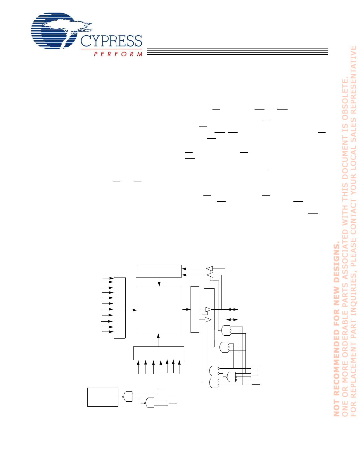
Logic Block Diagram
A
10
A
9
A
8
A
7
A
6
A
5
A
4
A
3
A
2
A
1
A
0
Power -Down
Circuit
Note:
1. For best practice recommendations, please refer to the Cypress application note “System Design Guidelines” on http://www.cypress.com.
DATA IN DRIVERS
256K x 16
RAM Array
ROW DECODER
COLUMN DECODER
11
A
A12A
I/O
–I/O
0
7
SENSE AMPS
CE
16
15
A
BHE
BLE
17
A
A
14
A
13
I/O8–I/O
15
BHE
WE
CE
OE
BLE
Cypress Semiconductor Corporation • 198 Champion Court • San Jose, CA 95134-1709 • 408-943-2600
Document #: 38-05340 Rev. *F Revised August 31, 2006
[+] Feedback
Page 2
CY62147DV30
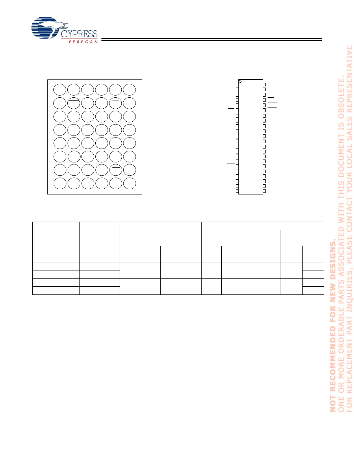
Pin Configuration
1
2
OE
BLE
I/O
BHE
8
I/O
I/O
V
V
I/O
I/O
NC
SS
CC
10
9
I/O
11
I/O
12
I/O
13
14
NC
15
A
8
[2, 3, 4]
VFBGA (Top View) 44 TSOP II (Top View)
4
3
A
0
A
3
A
5
A
17
DNU
A
14
A
12
A
9
5
6
A
A
1
A
4
A
6
A
7
A
16
A
15
A
13
A
10
CE
I/O
I/O
I/O
I/O
WE
A
NC
2
I/O
I/O
1
Vcc
3
Vss
4
I/O
5
I/O
NC
11
A
B
0
C
2
D
E
F
6
G
7
H
I/O
I/O
I/O
I/O
V
V
I/O
I/O
I/O
I/O
WE
A
A
A
A
A
A
A
A
A
A
CE
CC
SS
44
1
4
2
3
3
2
4
1
5
0
6
7
0
8
1
9
2
10
3
11
12
13
4
14
5
15
6
16
7
17
18
17
19
16
20
15
21
14
22
13
A
5
43
A
6
42
A
7
41
OE
40
BHE
39
BLE
38
I/O
37
I/O
36
I/O
35
I/O
34
V
SS
33
V
CC
32
I/O
31
I/O
30
I/O
29
I/O
NC
28
27
A
8
26
A
9
A
25
10
A
24
11
23
A
12
15
14
13
12
11
10
9
8
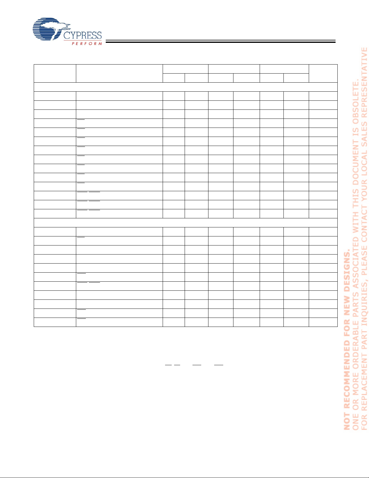
Product Portfolio
Power Dissipation
CC
CC
= V
(mA)
max
[5]
CC(typ.)
Standby I
Max. Typ.
, TA = 25°C.
(µA)Range f = 1MHz f = f
[5]
Max.
Operating I
[5]
Max. Typ.
Product VCC Range (V)
Min. Typ.
[5]
Speed
(ns)
Max. Typ.
CY62147DV30LL Industrial 2.2V 3.0 3.6 45 1.5 3 10 20 2 8
CY62147DV30LL Industrial 2.2V 3.0 3.6 55 1.5 3 8 15 2 8
CY62147DV30L Auto-E 25
CY62147DV30LL Industrial 2.2V 3.0 3.6 70 1.5 3 8 15 2 8
CY62147DV30LL Auto-A 8
Notes:
2. NC pins are not internally connected on the die.
3. DNU pins have to be left floating or tied to V
4. Pins H1, G2, and H6 in the VFBGA package are address expansion pins for 8 Mb, 16 Mb, and 32 Mb, respectively.
5. Typical values are included for reference only and are not guaranteed or tested. Typical values are measured at V
to ensure proper application.
SS
SB2
Document #: 38-05340 Rev. *F Page 2 of 12
[+] Feedback
Page 3
CY62147DV30
Maximum Ratings
(Above which the useful life may be impaired. For user guidelines, not tested.)
Storage Temperature .................................–65°C to +150°C
Ambient Temperature with
Power Applied.............................................–55°C to +125°C
Supply Voltage to Ground
Potential......................................–0.3V to + V
DC Voltage Applied to Outputs
in High-Z State
DC Input Voltage
[6,7]
..........................–0.3V to V
[6,7]
..................... –0.3V to V
CC(MAX)
CC(MAX)
CC(MAX)
+ 0.3V
+ 0.3V
+ 0.3V
Electrical Characteristics (Over the Operating Range)
Parameter Description Test Conditions
V
V
V
V
I
IX
I
OZ
I
CC
I
SB1
I
SB2
OH
OL
IH
IL
Output HIGH
Voltage
Output LOW
Voltage
Input HIGH
Voltage
Input LOW
Voltage
Input Leakage
Current
Output
Leakage
Current
VCC Operating
Supply
Current
Automatic CE
Power-Down
Current —
CMOS Inputs
Automatic CE
Power-Down
Current —
CMOS Inputs
IOH = –0.1 mA V
= –1.0 mA V
I
OH
IOL = 0.1 mA V
= 2.1 mA V
I
OL
V
= 2.2V to 2.7V 1.8 V
CC
= 2.7V to 3.6V 2.2 V
V
CC
V
= 2.2V to 2.7V –0.3 0.6 –0.3 0.6 V
CC
= 2.7V to 3.6V –0.3 0.8 –0.3 0.8 V
V
CC
GND < VI < V
CC
= 2.20V 2.0 2.0 V
CC
= 2.70V 2.4 2.4 V
CC
= 2.20V 0.4 0.4 V
CC
= 2.70V 0.4 0.4 V
CC
Ind’l
Auto-A
Auto-E
GND <
VO < VCC,
Output Disabled
Ind’l
Auto-A
Auto-E
f = f
f = 1 MHz 1.5 3 1.5 3 mA
CE
V
f = f
Data Only),
f = 0 (OE
BLE
CE > VCC – 0.2V,
V
V
f = 0, V
= 1/t
MAX
RC
> VCC−0.2V,
–0.2V, VIN<0.2V)
IN>VCC
(Address and
MAX
, WE, BHE and
), V
= 3.60V
CC
> VCC – 0.2V or
IN
< 0.2V,
IN
= 3.60V
CC
V
= V
CC
I
= 0 mA
OUT
CMOS levels
Ind’l LL 8 8 µA
Auto-A
Auto-E
Ind’l LL 8 8 µA
Auto-A
Auto-E
Output Current into Outputs (LOW).............................20 mA
Static Discharge Voltage........................................... >2001V
(per MIL-STD-883, Method 3015)
Latch-up Current......................................................>200 mA
Operating Range
Ambient
Device Range
Temperature
CY62147DV30L Automotive-E –40°C to +125°C 2.20V
CY62147DV30LL Industrial –40°C to +85°C
Automotive-A –40°C to +85°C
–45 –55/–70
[5]
Max. Min. Typ.
+ 0.3V 1.8 V
CC
+ 0.3V 2.2 V
CC
–1 +1 –1 +1 µA
[9]
[9]
–1 +1 µA
–4 +4 µA
–1 +1 –1 +1 µA
[9]
[9]
CCmax
[9]
LL 8
[9]
L25
[9]
LL 8
[9]
L25
10 20 8 15 mA
–1 +1 µA
–4 +4 µA
[TA]
[5]
[9]
CC
CC
3.60V
Max.
+ 0.3V V
+ 0.3V V
V
CC
to
UnitMin. Typ.
Notes:
6. V
7. V
8. Full device AC operation assumes a 100-µs ramp time from 0 to V
9. Auto-A is available in –70 and Auto-E is available in –55.
= –2.0V for pulse durations less than 20 ns.
IL(min.)
= V
IH(max.)
+ 0.75V for pulse durations less than 20 ns.
CC
(min) and 200-µs wait time after V
CC
stabilization.
CC
Document #: 38-05340 Rev. *F Page 3 of 12
[+] Feedback
Page 4
CY62147DV30
Capacitance (for all p ackages)
[10]
Parameter Description Test Conditions Max. Unit
C
IN
C
OUT
Thermal Resistance
Input Capacitance TA = 25°C, f = 1 MHz,
V
= V
CC
Output Capacitance 10 pF
[10]
CC(typ)
10 pF
Parameter Description Test Conditions VFBGA TSOP II Unit
Θ
JA
Θ
JC
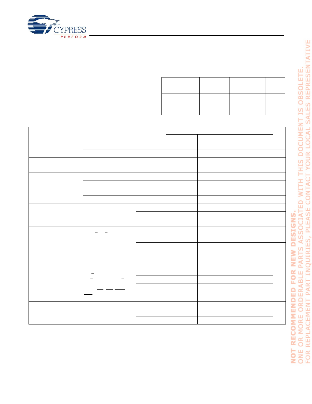
AC Test Loads and Waveforms
Thermal Resistance
(Junction to Ambient)
Thermal Resistance
(Junction to Case)
R1
CC
OUTPUT
50 pF
Still Air , soldered on a 3 × 4.5 inch, four-layer
printed circuit board
[10]
Rise Time = 1 V/ns
R2
VCC V
GND
10%
ALL INPUT PULSES
90%
72 75.13 °C/W
8.86 8.95 °C/W
90%
10%
Fall Time = 1 V/ns
INCLUDING
JIG AND
SCOPE
Equivalent to: THÉ VENIN EQUIVALENT
R
TH
OUTPUT V
Parameters 2.50V 3.0V Unit
R1 16667 1103 Ω
R2 15385 1554 Ω
R
TH
V
TH
8000 645 Ω
1.20 1.75 V
Data Retention Characteristics (Over the Operating Range)
Parameter Description Conditions Min. Typ.
V
DR
I
CCDR
[10]
t
CDR
[12]
t
R
Data Retention Waveform
CE or
BHE
VCC for Data Retention 1.5 V
Data Retention Current VCC= 1.5V
CE
> VCC – 0.2V ,
V
> VCC – 0.2V or
IN
V
< 0.2V
IN
Chip Deselect to Data Retention
L (Auto-E) 15 µA
LL (Ind’l/Auto-A) 6
0 ns
Time
Operation Recovery Time t
[13]
DATA RETENTION MODE
VDR> 1.5 V
V
CC
.BLE
V
CC(min)
t
CDR
RC
V
CC(min)
t
R
[5]
Max. Unit
ns
Notes:
10.Tested initially and after any design or process changes that may affect these parameters.
11.Test condition for the 45-ns part is a load capacitance of 30 pF.
12.Full device operation requires linear V
13.BHE
.BLE is the AND of both BHE and BLE. Chip can be deselected by either disabling the chip enable signals or by disabling both BHE and BLE.
ramp from V
CC
DR
to V
> 100 µs or stab le at V
CC(min.)
CC(min.)
> 100 µs.
Document #: 38-05340 Rev. *F Page 4 of 12
[+] Feedback
Page 5
CY62147DV30
Switching Characteristics Over the Operating Range
45 ns
Parameter Description
Read Cycle
t
RC
t
AA
t
OHA
t
ACE
t
DOE
t
LZOE
t
HZOE
t
LZCE
t
HZCE
t
PU
t
PD
t
DBE
t
LZBE
t
HZBE
Write Cycle
t
WC
t
SCE
t
AW
t
HA
t
SA
t
PWE
t
BW
t
SD
t
HD
t
HZWE
t
LZWE
Read Cycle Time 45 55 70 ns
Address to Data Valid 45 55 70 ns
Data Hold from Address Change 10 10 10 ns
CE LOW to Data Valid 45 55 70 ns
OE LOW to Data Valid 25 25 35 ns
OE LOW to LOW Z
OE HIGH to High Z
CE LOW to Low Z
CE HIGH to High Z
[15]
[15, 16]
[15]
[15, 16]
5 5 5 ns
10 10 10 ns
CE LOW to Power-Up 0 0 0 ns
CE HIGH to Power-Down 45 55 70 ns
BLE/BHE LOW to Data Valid 45 55 70 ns
BLE/BHE LOW to Low Z
BLE/BHE HIGH to HIGH Z
[17]
[15]
10 10 10 ns
[15, 16]
Write Cycle Time 45 55 70 ns
CE LOW to Write End 40 40 60 ns
Address Set-up to Write End 40 40 60 ns
Address Hold from Write End 0 0 0 ns
Address Set-up to Write Start 0 0 0 ns
WE Pulse Width 35 40 45 ns
BLE/BHE LOW to Write End 40 40 60 ns
Data Set-up to Write End 25 25 30 ns
Data Hold from Write End 0 0 0 ns
WE LOW to High-Z
WE HIGH to Low-Z
[15, 16]
[15]
10 10 10 ns
[14]
[11]
55 ns 70 ns
15 20 25 ns
20 20 25 ns
15 20 25 ns
15 20 25 ns
UnitMin. Max. Min. Max. Min. Max.
Notes:
14.Test conditions for all parameters other than tri-state p arameters assume signal transit ion time of 3 ns (1 V/ ns) or less, timing reference levels of V
pulse levels of 0 to V
15.At any given temperature and voltage condition, t
given device.
16.t
, t
HZCE
, t
HZBE
HZOE
17.The internal Write time of the memory is defined by the overlap of WE
of these signals can terminate a write by going INACTIVE. The data input set-up and ho ld timing should be reference d to the edge of t he signal that termina tes
the write.
, and output loading of the specified IOL/IOH as shown in the “AC Test Loads and Waveforms” section.
CC(typ.)
, and t
transitions are measured when the outputs enter a high impedence state.
HZWE
is less than t
HZCE
, t
LZCE
is less than t
HZBE
, CE = VIL, BHE and/or BLE = VIL. All signals must be ACTIVE to initiate a write and any
LZBE
, t
HZOE
is less than t
LZOE
, and t
is less than t
HZWE
CC(typ)
LZWE
/2, input
for any
Document #: 38-05340 Rev. *F Page 5 of 12
[+] Feedback
Page 6

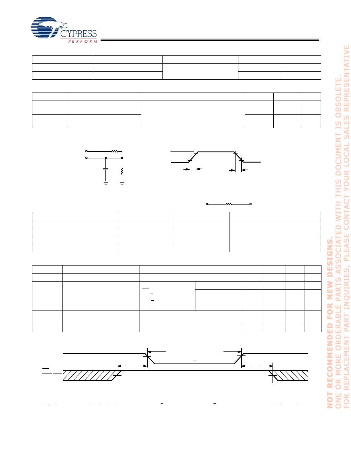
Switching Waveforms
t
OHA
[18, 19]
t
AA
t
RC
Read Cycle 1 (Address Transition Controlled)
ADDRESS
DATA OUT PREVIOUS DATA VALID DATA VALID
CY62147DV30
Read Cycle No. 2 (OE Controlled)
ADDRESS
CE
OE
BHE/BLE
t
LZBE
DATA OUT
V
CC
SUPPLY
HIGH IMPEDANCE
t
LZCE
t
PU
CURRENT
Notes:
18.The device is continuously selected. OE
is HIGH for read cycle.
19.WE
20.Address valid prior to or coincident with CE
[19, 20]
t
t
ACE
t
DOE
t
LZOE
t
DBE
50%
, CE = VIL, BHE and/or BLE = VIL.
and BHE, BLE transition LOW.
RC
DATA VALID
t
HZBE
t
HZCE
t
HZOE
t
PD
HIGH
IMPEDANCE
I
50%
CC
I
SB
Document #: 38-05340 Rev. *F Page 6 of 12
[+] Feedback
Page 7
Switching Waveforms (continued)
Write Cycle No. 1 (WE Controlled)
ADDRESS
CE
[17, 21, 22]
t
SCE
t
CY62147DV30
WC
WE
BHE/BLE
OE
DATA I/O
NOTE
23
Write Cycle No. 2 (CE Controlled)
ADDRESS
CE
WE
t
SA
t
HZOE
[17, 21, 22]
t
AW
t
PWE
t
BW
t
SD
DATA
IN
t
WC
t
SCE
t
SA
t
AW
t
PWE
t
HA
t
HD
t
HA
t
BHE/BLE
BW
OE
DATA I/O
Notes:
21.Data I/O is high impedance if OE
goes HIGH simultaneously with WE = VIH, the output remains in a high-impedance state.
22.If CE
23.During this period, the I/Os are in output state and input signals should not be applied.
NOTE
23
= VIH.
t
HZOE
t
SD
DATA
IN
t
HD
Document #: 38-05340 Rev. *F Page 7 of 12
[+] Feedback
Page 8

Switching Waveforms (continued)
Write Cycle No. 3 (WE Controlled, OE LOW)
ADDRESS
CE
BHE/BLE
[22]
t
t
SCE
BW
t
CY62147DV30
WC
t
SA
WE
DATAI/O
NOTE 23
t
HZWE
Write Cycle No. 4 (BHE/BLE Controlled, OE LOW)
ADDRESS
CE
BHE/BLE
t
SA
WE
t
HZWE
DATA I/O
NOTE 23
[22]
t
AW
t
AW
t
PWE
t
SD
t
HA
t
HD
DATAIN
t
LZWE
t
WC
t
SCE
t
HA
t
BW
t
PWE
t
SD
DATA
IN
t
HD
t
LZWE
Document #: 38-05340 Rev. *F Page 8 of 12
[+] Feedback
Page 9

CY62147DV30
Truth Table
CE WE OE BHE BLE Inputs/Outputs Mode Power
H X X X X High Z Deselect/Power-Down Standby (I
X X X H H High Z Deselect/Power-Down Standby (I
L H L L L Data Out (I/O
L H L H L Data Out (I/O
I/O
–I/O
8
L H L L H Data Out (I/O8–I/O15);
I/O
–I/O7 in High Z
0
L H H L L High Z Output Disabled Active (ICC)
L H H H L High Z Ou tpu t Disabled Active (I
L H H L H High Z Output Disabled Active (I
L L X L L Data In (I/O
L L X H L Data In (I/O
–I/O
I/O
8
L L X L H Data In (I/O
I/O
–I/O7 in High Z
0
–I/O15) Read Active (ICC)
O
in High Z
15
–I/O7);
O
Read Active (I
Read Active (I
–I/O15) Write Active (ICC)
O
O
in High Z
15
8
–I/O7);
–I/O15);
Write Active (I
Write Active (I
CC
CC
CC
CC
CC
CC
SB
SB
)
)
)
)
)
)
)
)
Ordering Information
Speed
(ns) Ordering Code
45 CY62147DV30LL-45BVXI 51-85150 48-ball (6 mm × 8mm × 1 mm) VFBGA (Pb-free) Industrial
CY62147DV30LL-45ZSXI 51-85087 44-pin TSOP II (Pb-free)
55 CY62147DV30LL-55BVI 51-85150 48-ball (6 mm × 8mm × 1 mm) VFBGA Industrial
CY62147DV30LL-55BVXI 48-ball (6 mm × 8mm × 1 mm) VFBGA (Pb-free)
CY62147DV30LL-55ZSXI 51-85087 44-pin TSOP II (Pb-free)
CY62147DV30L-55BVXE 51-85150 48-ball (6 mm × 8mm × 1 mm) VFBGA (Pb-free) Automotive-E
CY62147DV30L-55ZSXE 51-85087 44-pin TSOP II (Pb-free)
70 CY62147DV30LL-70BVI 51-85150 48-ball (6 mm × 8mm × 1 mm) VFBGA Industrial
CY62147DV30LL-70BVXA 48-ball (6 mm × 8mm × 1 mm) VFBGA (Pb-free) Automotive-A
Package
Diagram Package Type
Operating
Range
Document #: 38-05340 Rev. *F Page 9 of 12
[+] Feedback
Page 10

Package Diagram
A1 CORNER
TOP VIEW
CY62147DV30
48-ball VFBGA (6 x 8 x 1 mm) (51-85150)
BOTTOM VIEW
A1 CORNER
Ø0.05 M C
Ø0.25 M C A B
Ø0.30±0.05(48X)
465231
65
1
234
0.25 C
8.00±0.10
A
0.55 MAX.
0.26 MAX.
A
B
C
D
E
F
G
H
A
B
6.00±0.10
0.21±0.05
0.10 C
8.00±0.10
5.25
0.75
0.15(4X)
2.625
1.875
0.75
3.75
B
6.00±0.10
A
B
C
D
E
F
G
H
51-85150-*D
SEATING PLANE
C
1.00 MAX
Document #: 38-05340 Rev. *F Page 10 of 12
[+] Feedback
Page 11
Package Diagram (continued)
CY62147DV30
44-Pin TSOP II (51-85087)
51-85087-*A
MoBL is a registered trademark, and More Battery Life is a trademark, of Cypress Semicond uctor Corporatio n. All product a nd
company names mentioned in this document may be the trademarks of their respective holders.
Document #: 38-05340 Rev. *F Pa ge 11 of 12
© Cypress Semiconductor Corporation, 20 06 . The i nfo r ma tion con tained herein is subject to change without n oti ce. C ypr ess S em i conductor Corpo ration assu mes no resp onsibility f or the u se
of any circuitry other than circuitry embodied in a Cypress product. Nor does it convey or imply any license under patent or other rights. Cypress products are not warranted nor intended to be
used for medical, life support, life saving, critical control or safety applications, unless pursuant to an express written agreement with Cypress. Furtherm ore, Cypress doe s not authorize i ts
products for use as critical components in life-support systems where a malfunction or failure may reasonably be expected to result in significant injury to the user. The inclusion of Cypress
products in life-support systems application implies that the manufacturer assumes all risk of such use and in doing so indemnifies Cypress against all charges.
[+] Feedback
Page 12

CY62147DV30
Document History Page
Document Title:CY62147DV30 MoBL® 4-Mbit (256K x 16) Static RAM
Document Number: 38-05340
REV. ECN NO. Issue Date
** 127481 06/17/03 HRT New Data Sheet
*A 131010 01/23/04 CBD Changed from Advance to Preliminary
*B 213252 See ECN AJU Changed from Preliminary to Final
*C 257349 See ECN PCI Modified ordering information for 70-ns Speed Bin
*D 316039 See ECN PCI Added 45-ns Speed Bin in AC, DC and Ordering Information tables
*E 330365 See ECN AJU Added Automotive product information
*F 498575 See ECN NXR Added Automotive-A range
Orig. of
Change Description of Change
Added 70 ns speed bin
Modified footnote 7 to include ramp time and wait time
Modified input and output capacitance values to 10 pF
Modified Thermal Resistance values on page 4
Added “Byte power-down feature” in the features section
Modified Ordering Information for Pb-free parts
Added Footnote #10 on page #4
Added Pb-free package ordering information on page # 9
Changed 44-lead TSOP-II package name on page 11 from Z44 to ZS44
Standardized Icc values across ‘L’ and ‘LL’ bins
Added note# 9 on page# 3
Updated ordering information table
Document #: 38-05340 Rev. *F Page 12 of 12
[+] Feedback
 Loading...