

Page 1
CY62146DV30
4-Mbit (256K x 16) Static RAM
Features
• Very high speed: 45 ns
• Wide voltage range: 2.20V–3.60V
• Pin-compatible with CY62146CV30
• Ultra-low active power
— Typical active current: 1.5 mA @ f = 1 MHz
— Typical active current: 8 mA @ f = f
max
• Ultra low standby power
• Easy memory expansion with CE
, and OE features
• Automatic power-down when deselected
• CMOS for optimum speed/power
• Packages offered 48-ball BGA and 44-pin TSOPII
• Also available in Lead-free packages
Functional Description
[1]
The CY62146DV30 is a high-performance CMOS static RAM
organized as 256K words by 16 bits. This device features advanced circuit design to provide ultra-low active current. This
is ideal for providing More Battery Life™ (MoBL
) in portable
applications such as cellular telephones. The device also has
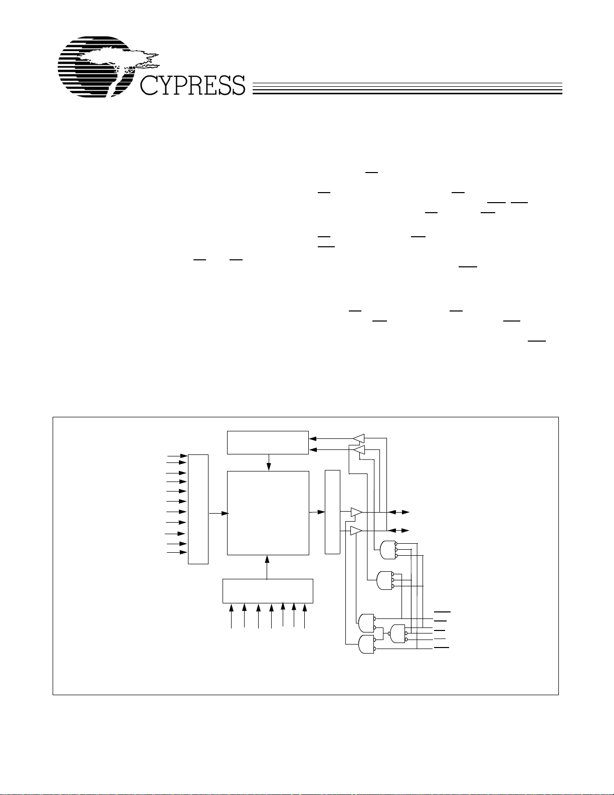
Logic Block Diagram
DATA IN DRIVERS
A
10
A
9
A
8
A
7
A
6
A
5
A
4
A
3
A
2
A
1
A
0
ROW DECODER
256K x 16
RAM Array
an automatic power-down feature that significantly reduces
power consumption. The device can also be put into standby
mode reducing power consumption by more than 99% when
deselected (CE
I/O
) are placed in a high-impedance state when: deselected
15
(CE
HIGH), outputs are disabled (OE HIGH), both Byte High
Enable and Byte Low Enable are disabled (BHE
or during a write operation (CE
HIGH). The input/output pins (I/O0 through
, BLE HIGH),
LOW and WE LOW).
Writing to the device is accomplished by taking Chip Enable
(CE
) and Write Enable (WE) inputs LOW. If Byte Low Enable
(BLE
) is LOW, then data from I/O pins (I/O0 through I/O7), is
written into the location specified on the address pins (A
through A17). If Byte High Enable (BHE) is LOW, then data
from I/O pins (I/O
specified on the address pins (A
through I/O15) is written into the location
8
through A17).
0
Reading from the device is accomplished by taking Chip
Enable (CE
Write Enable (WE
) and Output Enable (OE) LOW while forcing the
) HIGH. If Byte Low Enable (BLE) is LOW,
then data from the memory location specified by the address
pins will appear on I/O0 to I/O7. If Byte High Enable (BHE) is
LOW, then data from memory will appear on I/O
the truth table at the back of this data sheet for a complete
to I/O15. See
8
description of read and write modes.
The CY62146DV30 is available in a 48-ball VFBGA, 44-pin
TSOPII packages.
–I/O
I/O
0
7
SENSE AMPS
I/O8–I/O
15
0
COLUMN DECODER
BHE
11
13
A
A12A
Note:
1. For best practice recommendations, please refer to the Cypress application note “System Design Guidelines” on http://www.cypress.com.
16
15
14
A
17
A
A
A
WE
CE
OE
BLE
Cypress Semiconductor Corporation • 3901 North First Street • San Jose, CA 95134 • 408-943-2600
Document #: 38-05339 Rev. *A Revised February 2, 2005
[+] Feedback
Page 2
CY62146DV30
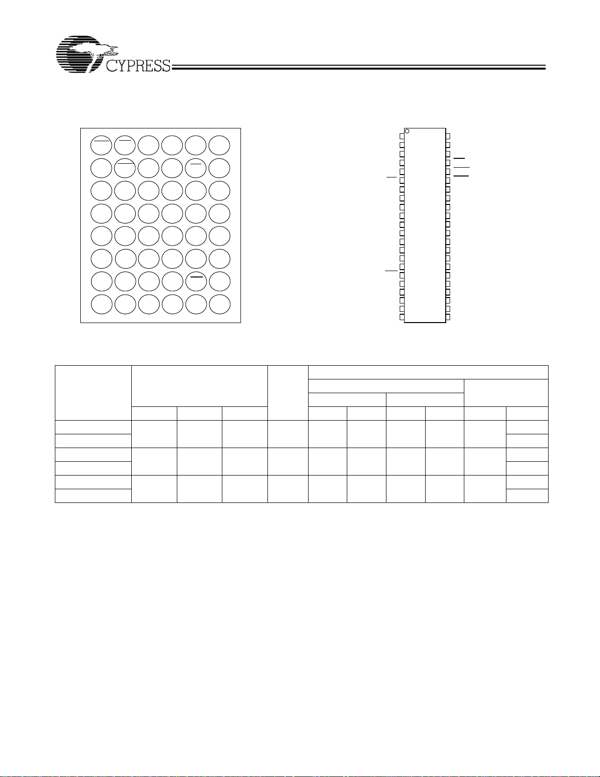
Pin Configuration
[2, 3, 4]
VFBGA (Top View) 44 TSOP II (Top View)
1
BLE
I/O
I/O
V
SS
V
CC
I/O
I/O
NC
2
OE
BHE
8
I/O
10
9
I/O
11
DNU
I/O
12
I/O
13
14
NC
15
A
8
4
3
A
0
A
3
A
5
A
17
A
14
A
12
A
9
5
6
A
A
1
A
4
A
6
A
7
A
16
A
15
A
13
A
10
CE
I/O
I/O
I/O
I/O
WE
A
NC
2
I/O
I/O
1
Vcc
3
Vss
4
I/O
5
I/O
NC
11
A
B
0
C
2
D
E
F
6
G
7
H
I/O
I/O
I/O
I/O
V
V
I/O
I/O
I/O
I/O
WE
A
A
A
A
A
A
A
A
A
A
CE
CC
SS
44
1
4
2
3
3
2
4
1
5
0
6
7
0
8
1
9
2
10
3
11
12
13
4
14
5
15
6
16
7
17
18
17
19
16
20
15
21
14
22
13
A
5
43
A
6
42
A
7
41
OE
40
BHE
39
BLE
38
I/O
15
37
I/O
14
36
I/O
13
35
I/O
12
34
V
SS
33
V
CC
32
I/O
11
I/O
31
10
30
I/O
9
29
I/O
8
NC
28
27
A
8
26
A
9
25
A
10
A
24
11
23
A
12
Product Portfolio
Power Dissipation
Operating I
Range (V)
V
Product
CC
Min. Typ.
[5]
Max. Typ.
Speed
(ns)
[5]
Max. Typ.
CY62146DV30L 2.20V 3.0 3.60 45 1.5 3 10 20 2 12
CY62146DV30LL 8
CY62146DV30L 2.20V 3.0 3.60 55 1.5 3 8 15 2 12
CY62146DV30LL 8
CY62146DV30L 2.20V 3.0 3.60 70 1.5 3 8 15 2 12
CY62146DV30LL 8
CC
(mA)
[5]
max
Max. Typ.
Standby I
[5]
SB2
Max.
(µA)f = 1MHz f = f
Notes:
2. NC pins are not internally connected on the die.
3. DNU pins have to be left floating or tied to V
4. Pins H1, G2, and H6 in the BGA package are address expansion pins for 8 Mb, 16 Mb, and 32 Mb, respectively.
5. Typical values are included for reference only and are not guaranteed or tested. Typical values are measured at V
to ensure proper application.
SS
CC
= V
CC(typ.)
, TA = 25°C.
Document #: 38-05339 Rev. *A Page 2 of 11
[+] Feedback
Page 3
CY62146DV30
Maximum Ratings
(Above which the useful life may be impaired. For user guidelines, not tested.)
Storage Temperature .................................–65°C to +150°C
Ambient Temperature with
Power Applied.............................................–55°C to +125°C
Supply Voltage to Ground
Potential......................................–0.3V to + V
DC Voltage Applied to Outputs
in High-Z State
[6, 7]
.........................–0.3V to V
CC(MAX)
CC(MAX)
+ 0.3V
+ 0.3V
Electrical Characteristics Over the Operating Range
CY62146DV30-45 CY62146DV30-55 CY62146DV30-70
Parameter Description Test Conditions
V
OH
V
OL
V
IH
V
IL
I
IX
I
OZ
I
CC
I
SB1
I
SB2
Notes:
6. V
7. V
8. Full device AC operation assumes a 100-µs ramp time from 0 to V
Output HIGH
Voltage
Output LOW
Voltage
Input HIGH
Voltage
Input LOW
Voltage
Input Leakage
IOH = –0.1 mA V
I
= –1.0 mA V
OH
IOL = 0.1 mA V
I
= 2.1 mA V
OL
V
= 2.2V to 2.7V 1.8 V
CC
= 2.7V to 3.6V 2.2 V
V
CC
V
= 2.2V to 2.7V –0.3 0.6 –0.3 0.6 –0.3 0.6 V
CC
VCC= 2.7V to 3.6V –0.3 0.8 –0.3 0.8 –0.3 0.8 V
GND < VI < V
Current
Output
Leakage
GND < VO < VCC, Output
Disabled
Current
VCC
Operating
Supply
Current
Automatic
CE
Power-down
Current —
CMOS
Inputs
Automatic
CE
Power-down
Current —
CMOS Inputs
= –2.0V for pulse durations less than 20 ns.
IL(min.)
= VCC+0.75V for pulse durations less than 20 ns.
IH(max)
f = f
1/t
RC
MAX
=
f = 1 MHz 1.5 3 1.5 3 1.5 3 mA
CE
> VCC−0.2V,
V
f = f
Only),
–0.2V, VIN<0.2V)
IN>VCC
(Address and Data
MAX
f = 0 (OE
), V
BLE
CE
V
0.2V,
f = 0, V
CC
> VCC – 0.2V,
> VCC – 0.2V or VIN <
IN
CC
= 2.20V 2.0 2.0 2.0 V
CC
= 2.70V 2.4 2.4 2.4 V
CC
= 2.20V 0.4 0.4 0.4 V
CC
= 2.70V 0.4 0.4 0.4 V
CC
CC
VCC = V
I
OUT
CMOS levels
CCmax
= 0 mA
, WE, BHE and
= 3.60V
= 3.60V
–1 +1 –1 +1 –1 +1 µA
–1 +1 –1 +1 –1 +1 µA
L212 212 212µA
LL 8 8 8
L212 212 212µA
LL 8 8 8
(min) and 200 µs wait time after V
CC
DC Input Voltage
[6, 7]
.....................–0.3V to V
CC(MAX)
+ 0.3V
Output Current into Outputs (LOW)............................. 20 mA
Static Discharge Voltage........................................... >2001V
(per MIL-STD-883, Method 3015)
Latch-up Current......................................................>200 mA
Operating Range
Device Range
perature (TA)V
CY62146DV30L Industrial –40°C to +85°C 2.20V to 3.60V
CY62146DV30LL
Ambient Tem-
[5]
Max. Min. Typ.
+
CC
0.3V
+
CC
0.3V
1.8 V
2.2 V
[5]
Max. Min. Typ.
+
CC
0.3V
+
CC
0.3V
[5]
1.8 V
2.2 V
10 20 8 15 8 15 mA
stabilization.
CC
CC
Max.
CC
0.3V
CC
0.3V
[8]
UnitMin. Typ.
+
V
+
V
Document #: 38-05339 Rev. *A Page 3 of 11
[+] Feedback
Page 4
CY62146DV30
Capacitance (for all packages)
[9]
Parameter Description Test Conditions Max. Unit
C
IN
C
OUT
Thermal Resistance
Input Capacitance TA = 25°C, f = 1 MHz,
= V
V
CC
Output Capacitance 10 pF
[9]
CC(typ)
10 pF
Parameter Description Test Conditions BGA TSOP II Unit
Θ
JA
Θ
JC
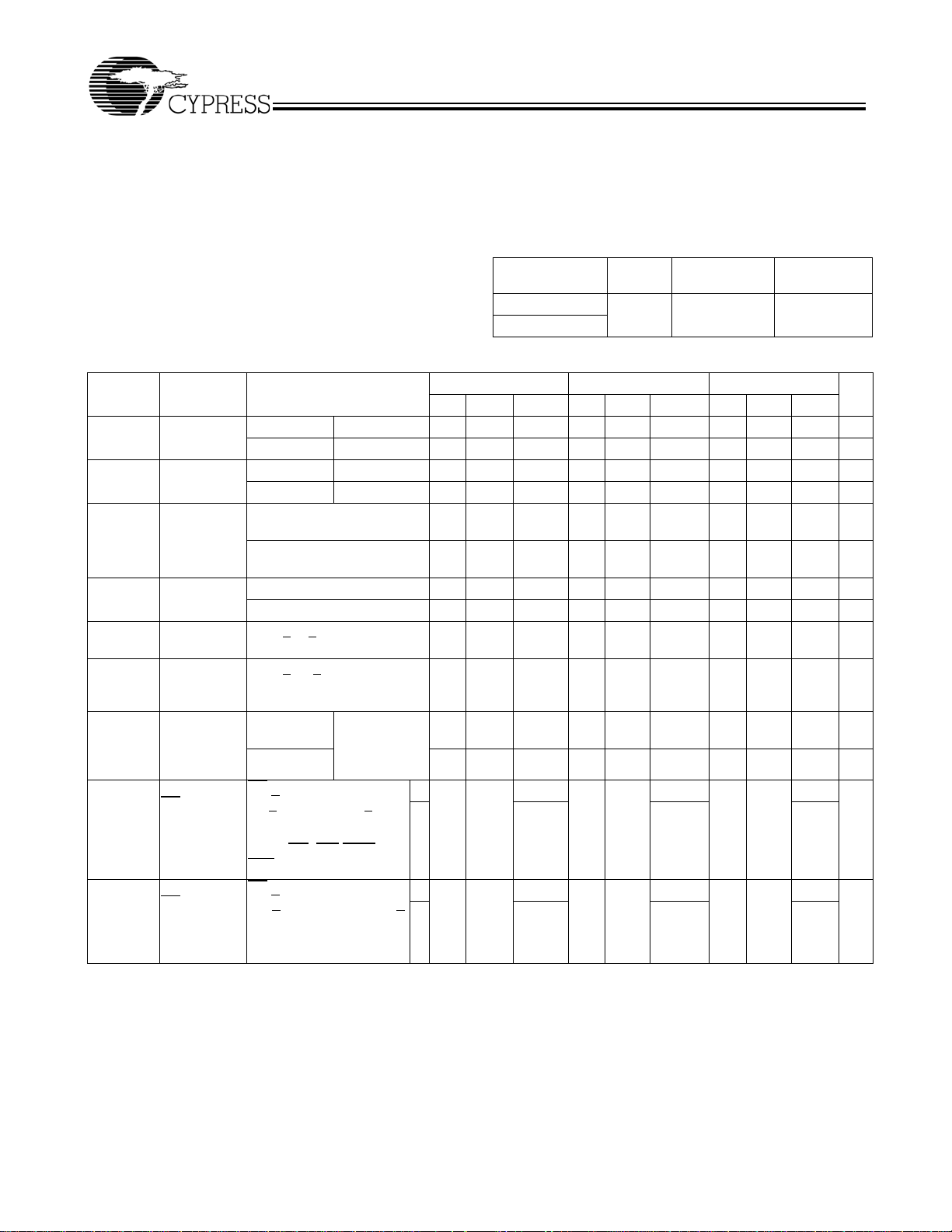
AC Test Loads and Waveforms
Thermal Resistance
(Junction to Ambient)
Thermal Resistance
(Junction to Case)
R1
V
CC
OUTPUT
50 pF
Still Air, soldered on a 3 × 4.5 inch, four-layer
printed circuit board
[10]
Rise Time = 1 V/ns
R2
VCC
GND
10%
ALL INPUT PULSES
90%
72 75.13 °C/W
8.86 8.95 °C/W
90%
10%
Fall Time = 1 V/ns
INCLUDING
JIG AND
SCOPE
Equivalent to: THÉ VENIN EQUIVALENT
R
TH
OUTPUT V
Parameters 2.50V 3.0V Unit
R1 16667 1103 Ω
R2 15385 1554 Ω
R
TH
V
TH
8000 645 Ω
1.20 1.75 V
Data Retention Characteristics (Over the Operating Range)
Parameter Description Conditions Min. Typ.
V
I
CCDR
t
CDR
t
R
DR
[9]
[11]
VCC for Data Retention 1.5 V
Data Retention Current VCC= 1.5V
CE
> VCC – 0.2V,
V
> VCC – 0.2V or VIN < 0.2V
IN
L9µA
LL 6
Chip Deselect to Data Retention Time 0 ns
Operation Recovery Time t
RC
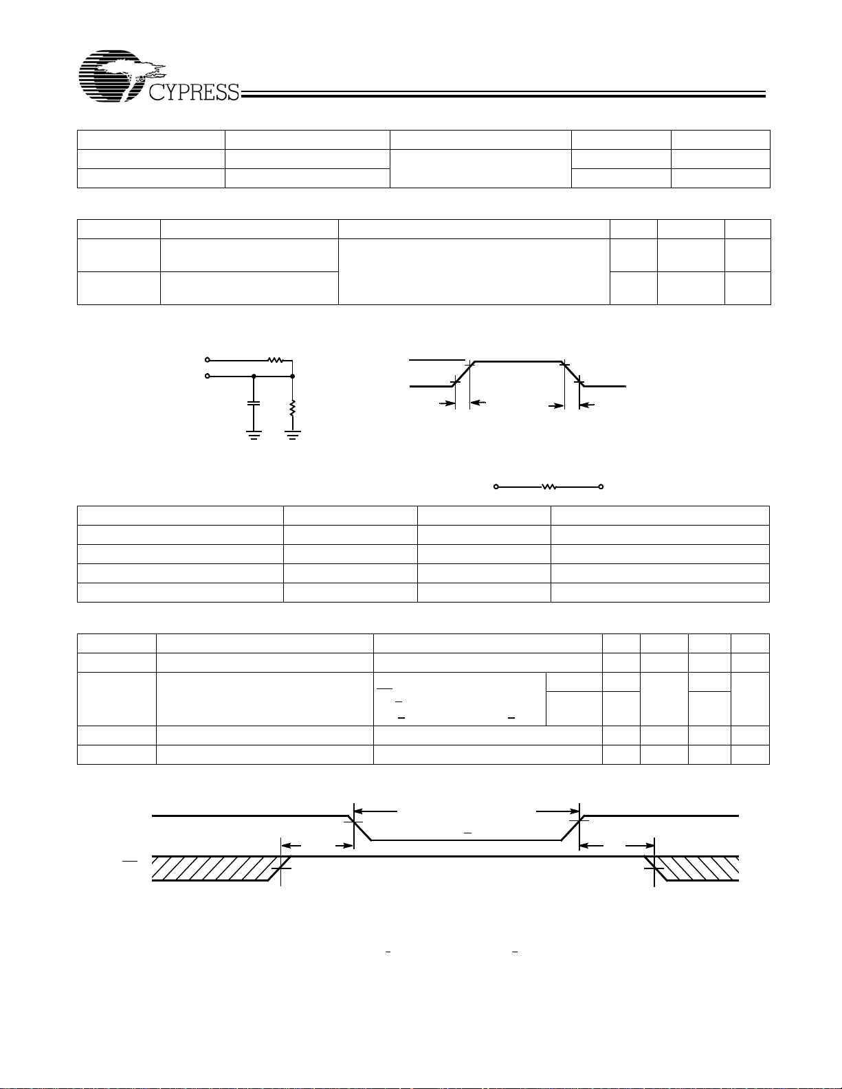
Data Retention Waveform
DATA RETENTION MODE
VDR> 1.5 V
V
CC(min)
t
R
V
CE
CC
V
CC(min)
t
CDR
[5]
Max. Unit
ns
Notes:
9. Tested initially and after any design or process changes that may affect these parameters.
10. Test condition for the 45 ns part is a load capacitance of 30 pF.
11.Full device operation requires linear V
ramp from V
CC
DR
to V
> 100 µs or stable at V
CC(min.)
CC(min.)
> 100 µs.
Document #: 38-05339 Rev. *A Page 4 of 11
[+] Feedback
Page 5

CY62146DV30
Switching Characteristics Over the Operating Range
[12]
45 ns
[10]
55 ns 70 ns
Parameter Description
Read Cycle
t
RC
t
AA
t
OHA
t
ACE
t
DOE
t
LZOE
t
HZOE
t
LZCE
t
HZCE
t
PU
t
PD
t
DBE
t
LZBE
t
HZBE
Write Cycle
t
WC
t
SCE
t
AW
t
HA
t
SA
t
PWE
t
BW
t
SD
t
HD
t
HZWE
t
LZWE
Notes:
12. Test conditions for all parameters other than three-state parameters assume signal transition time of 3 ns (1V/ns) or less, timing reference levels of V
input pulse levels of 0 to V
13. At any given temperature and voltage condition, t
given device.
, t
14. t
HZOE
15. The internal Write time of the memory is defined by the overlap of WE
of these signals can terminate a write by going INACTIVE. The data input set-up and hold timing should be referenced to the edge of the signal that terminates
the write.
Read Cycle Time 45 55 70 ns
Address to Data Valid 45 55 70 ns
Data Hold from Address Change 10 10 10 ns
CE LOW to Data Valid 45 55 70 ns
OE LOW to Data Valid 25 25 35 ns
OE LOW to LOW Z
OE HIGH to High Z
CE LOW to Low Z
CE HIGH to High Z
[13]
[13, 14]
[13]
[13, 14]
55 5ns
15 20 25 ns
10 10 10 ns
20 20 25 ns
CE LOW to Power-Up 0 0 0 ns
CE HIGH to Power-Down 45 55 70 ns
BLE/BHE LOW to Data Valid 25 25 35 ns
BLE/BHE LOW to Low Z
BLE/BHE HIGH to HIGH Z
[15]
[13]
[13, 14]
10 10 10 ns
15 20 25 ns
Write Cycle Time 45 55 70 ns
CE LOW to Write End 40 40 60 ns
Address Set-up to Write End 40 40 60 ns
Address Hold from Write End 0 0 0 ns
Address Set-up to Write Start 0 0 0 ns
WE Pulse Width 35 40 45 ns
BLE/BHE LOW to Write End 40 40 60 ns
Data Set-up to Write End 25 25 30 ns
Data Hold from Write End 0 0 0 ns
WE LOW to High-Z
WE HIGH to Low-Z
, t
HZBE
, and t
HZCE
CC(typ.)
transitions are measured when the outputs enter a high-impedence state.
HZWE
[13, 14]
[13]
, and output loading of the specified IOL/IOH as shown in the “AC Test Loads and Waveforms” section.
is less than t
HZCE
10 10 10 ns
, t
LZCE
HZBE
, CE = VIL, BHE and/or BLE = VIL. All signals must be ACTIVE to initiate a write and any
15 20 25 ns
is less than t
LZBE
, t
HZOE
is less than t
LZOE
, and t
HZWE
is less than t
LZWE
UnitMin. Max. Min. Max. Min. Max.
CC(typ)
for any
/2,
Document #: 38-05339 Rev. *A Page 5 of 11
[+] Feedback
Page 6

Switching Waveforms
t
OHA
t
DOE
[16, 17]
t
AA
t
RC
t
RC
Read Cycle 1 (Address Transition Controlled)
ADDRESS
DATA OUT PREVIOUS DATA VALID DATA VALID
Read Cycle No. 2 (OE Controlled)
ADDRESS
[17, 18]
CE
t
ACE
OE
BHE/BLE
t
LZOE
CY62146DV30
t
PD
t
HZCE
t
HZOE
t
LZBE
DATA OUT
V
CC
SUPPLY
HIGH IMPEDANCE
t
LZCE
t
PU
CURRENT
Notes:
16. The device is continuously selected. OE
17. WE
is HIGH for read cycle.
18. Address valid prior to or coincident with CE
t
DBE
50%
, CE = VIL, BHE and/or BLE = VIL.
and BHE, BLE transition LOW.
DATA VALID
t
HZBE
50%
HIGH
IMPEDANCE
I
CC
I
SB
Document #: 38-05339 Rev. *A Page 6 of 11
[+] Feedback
Page 7

Switching Waveforms (continued)
Write Cycle No. 1 (WE Controlled)
ADDRESS
CE
[15, 19, 20]
t
SCE
t
CY62146DV30
WC
WE
BHE/BLE
OE
DATA I/O
NOTE
21
Write Cycle No. 2 (CE Controlled)
ADDRESS
CE
WE
t
SA
t
HZOE
[15, 19, 20]
t
AW
t
PWE
t
BW
t
SD
DATA
IN
t
WC
t
SCE
t
SA
t
AW
t
PWE
t
HA
t
HD
t
HA
t
BHE/BLE
BW
OE
DATA I/O
Notes:
19. Data I/O is high impedance if OE
goes HIGH simultaneously with WE = VIH, the output remains in a high-impedance state.
20. If CE
21. During this period, the I/Os are in output state and input signals should not be applied.
NOTE
21
= VIH.
t
HZOE
t
SD
DATA
IN
t
HD
Document #: 38-05339 Rev. *A Page 7 of 11
[+] Feedback
Page 8

Switching Waveforms (continued)
Write Cycle No. 3 (WE Controlled, OE LOW)
ADDRESS
CE
BHE/BLE
[20]
t
t
BW
SCE
t
CY62146DV30
WC
t
SA
WE
DATAI/O
NOTE 21
t
HZWE
Write Cycle No. 4 (BHE/BLE Controlled, OE LOW)
ADDRESS
CE
BHE/BLE
t
SA
WE
t
HZWE
DATA I/O
NOTE 21
[20]
t
t
AW
AW
t
SCE
t
PWE
t
WC
t
PWE
t
BW
t
SD
DATAIN
t
SD
DATA
t
HA
t
HD
t
LZWE
t
HA
t
HD
IN
t
LZWE
Document #: 38-05339 Rev. *A Page 8 of 11
[+] Feedback
Page 9

CY62146DV30
Truth Table
CE WE OE BHE BLE Inputs/Outputs Mode Power
H X X X X High Z Deselect/Power-Down Standby (I
L X X H H High Z Output Disabled Active (I
L H L L L Data Out (I/O
L H L H L Data Out (I/O
–I/O
I/O
8
L H L L H Data Out (I/O
I/O
–I/O7 in High Z
0
L H H L L High Z Output Disabled Active (ICC)
L H H H L High Z Output Disabled Active (I
L H H L H High Z Output Disabled Active (I
L L X L L Data In (I/O
L L X H L Data In (I/O
I/O
–I/O
8
L L X L H Data In (I/O8–I/O15);
–I/O7 in High Z
I/O
0
Ordering Information
Speed
(ns) Ordering Code
45 CY62146DV30LL-45BVI BV48A 48-ball Very Fine Pitch BGA (6 mm × 8mm × 1 mm) Industrial
CY62146DV30LL-45BVXI 48-ball Very Fine Pitch BGA (6 mm × 8mm × 1 mm) (Pb-free)
CY62146DV30LL-45ZSXI ZS-44 44-pin TSOP II (Pb-free)
55 CY62146DV30L-55BVI BV48A 48-ball Very Fine Pitch BGA (6 mm × 8mm × 1 mm) Industrial
CY62146DV30L-55BVXI 48-ball Very Fine Pitch BGA (6 mm × 8mm × 1 mm)
CY62146DV30LL-55BVI 48-ball Very Fine Pitch BGA (6 mm × 8mm × 1 mm)
CY62146DV30LL-55BVXI 48-ball Very Fine Pitch BGA (6 mm × 8mm × 1 mm)
CY62146DV30L-55ZSXI ZS-44 44-pin TSOP II (Pb-free)
CY62146DV30LL-55ZSXI
70 CY62146DV30L-70BVI BV48A 48-ball Very Fine Pitch BGA (6 mm × 8mm × 1 mm) Industrial
CY62146DV30L-70BVXI 48-ball Very Fine Pitch BGA (6 mm × 8mm × 1 mm)
CY62146DV30LL-70BVI 48-ball Very Fine Pitch BGA (6 mm × 8mm × 1 mm)
CY62146DV30LL-70BVXI 48-ball Very Fine Pitch BGA (6 mm × 8mm × 1 mm)
CY62146DV30L-70ZSXI ZS-44 44-pin TSOP II (Pb-free) Industrial
CY62146DV30LL-70ZSXI
Package
Name Package Type
–I/O15) Read Active (ICC)
O
–I/O7);
O
in High Z
15
–I/O15);
8
–I/O15) Write Active (ICC)
O
–I/O7);
O
in High Z
15
Read Active (I
Read Active (I
Write Active (I
Write Active (I
(Pb-free)
(Pb-free)
(Pb-free)
(Pb-free)
)
SB
)
CC
)
CC
)
CC
)
CC
)
CC
)
CC
)
CC
Operating
Range
Document #: 38-05339 Rev. *A Page 9 of 11
[+] Feedback
Page 10

Package Diagram
CY62146DV30
48-Lead VFBGA (6 x 8 x 1 mm) BV48A
44-Pin TSOP II ZS44
51-85150-*B
51-85087-*A
MoBL is a registered trademark, and More Battery Life is a trademark, of Cypress Semiconductor. All product and company
names mentioned in this document may be the trademarks of their respective holders.
Document #: 38-05339 Rev. *A Page 10 of 11
© Cypress Semiconductor Corporation, 2005. The information contained herein is subject to change without notice. Cypress Semiconductor Corporation assumes no responsibility for the use
of any circuitry other than circuitry embodied in a Cypress product. Nor does it convey or imply any license under patent or other rights. Cypress products are not warranted nor intended to be
used for medical, life support, life saving, critical control or safety applications, unless pursuant to an express written agreement with Cypress. Furthermore, Cypress does not authorize its
products for use as critical components in life-support systems where a malfunction or failure may reasonably be expected to result in significant injury to the user. The inclusion of Cypress
products in life-support systems application implies that the manufacturer assumes all risk of such use and in doing so indemnifies Cypress against all charges.
[+] Feedback
Page 11

CY62146DV30
Document History Page
Document Title:CY62146DV30 MoBL® 4-Mbit (256K x 16) Static RAM
Document Number: 38-05339
REV. ECN NO. Issue Date
** 213251 See ECN AJU New Data Sheet
*A 316039 See ECN PCI Added 45-ns Speed Bin in AC, DC and Ordering Information tables
Orig. of
Change Description of Change
Added Footnote #10 on page #4
Added Pb-free package ordering information on page # 9
Changed 44-lead TSOP-II package name on page 10 from Z44 to ZS44
Standardized Icc values across ‘L’ and ‘LL’ bins
Document #: 38-05339 Rev. *A Page 11 of 11
[+] Feedback
 Loading...