查询CY62137CV供应商
Features
• Very high speed: 55 ns and 70 ns
• V oltage range:
—CY62137CV25: 2.2V–2.7V
—CY62137CV30: 2.7V–3.3V
—CY62137CV33: 3.0V–3.6V
—CY62137CV: 2.7V–3.6V
• Pin-compatible with the CY62137V
• Ultra-low active power
—Typical active current: 1.5 mA @ f = 1 MHz
—Typical active current: 5.5 mA @ f = f
speed)
• Low and ultra-low standby power
• Easy memory expansion with CE
and OE features
• Automatic power-down when deselected
• CMOS for optimum speed/power
• Packages offered in a 48-ball FBGA
Functional Description
[1]
The CY62137CV25/30/33 and CY62137CV are high-performance CMOS static RAMs organized as 128K words by 16
bits. These devic es feature advanced circuit de sign to pro vide
ultra-low active current. This is ideal for providing More Battery
max
(70-ns
CY62137CV25/30/33 MoBL
CY62137CV MoBL
2M (128K x 16) Static RAM
Life™ (MoBL®) in portable applications such as cellular telephones. The devices also has an automatic power-down feature that significantly reduces power consumption by 80%
when addresses are not toggling. The device can also be put
into standby m ode reduci ng power con sumption by more tha n
99% when deselected (CE
HIGH). The input/output pins (I/O
in a high-impedance state when: deselected (CE
puts are dis abled (OE HIGH), both Byte High Enable and Byte
Low Enable a r e d is a bled ( B HE
operation (CE
LOW, and WE LOW).
Writing to the device is accomplished by taking Chip Enable
) and Write Enable (WE) inputs LOW. If Byte Low Enable
(CE
(BLE) is LOW, then data from I/O pins (I/O0 through I/O7), is
written into the location specified on the address pins (A
through A16). If Byte High Enable (BHE) is LOW, then data
from I/O pins (I/O8 through I/O15) is written into the location
specified on the address pins (A
Reading from the device is accomplished by taking Chip
Enable (CE
Write Enable (WE
) and Output Enable (OE) LOW while forcing the
) HIGH. If Byte Low Enable (BLE) is LOW,
then data from the memory location specified by the address
pins will appear on I/O
LOW , then d ata f rom memory will a ppear on I/O
the truth table at the back of this data sheet for a complete
description of read and write modes.
HIGH or both BLE and BHE are
through I/O15) are plac ed
0
HIGH), out-
, BLE HIGH), or during a write
through A16).
0
to I/O7. If Byte High Enable (BHE) is
0
to I/O15. See
8
®
®
0
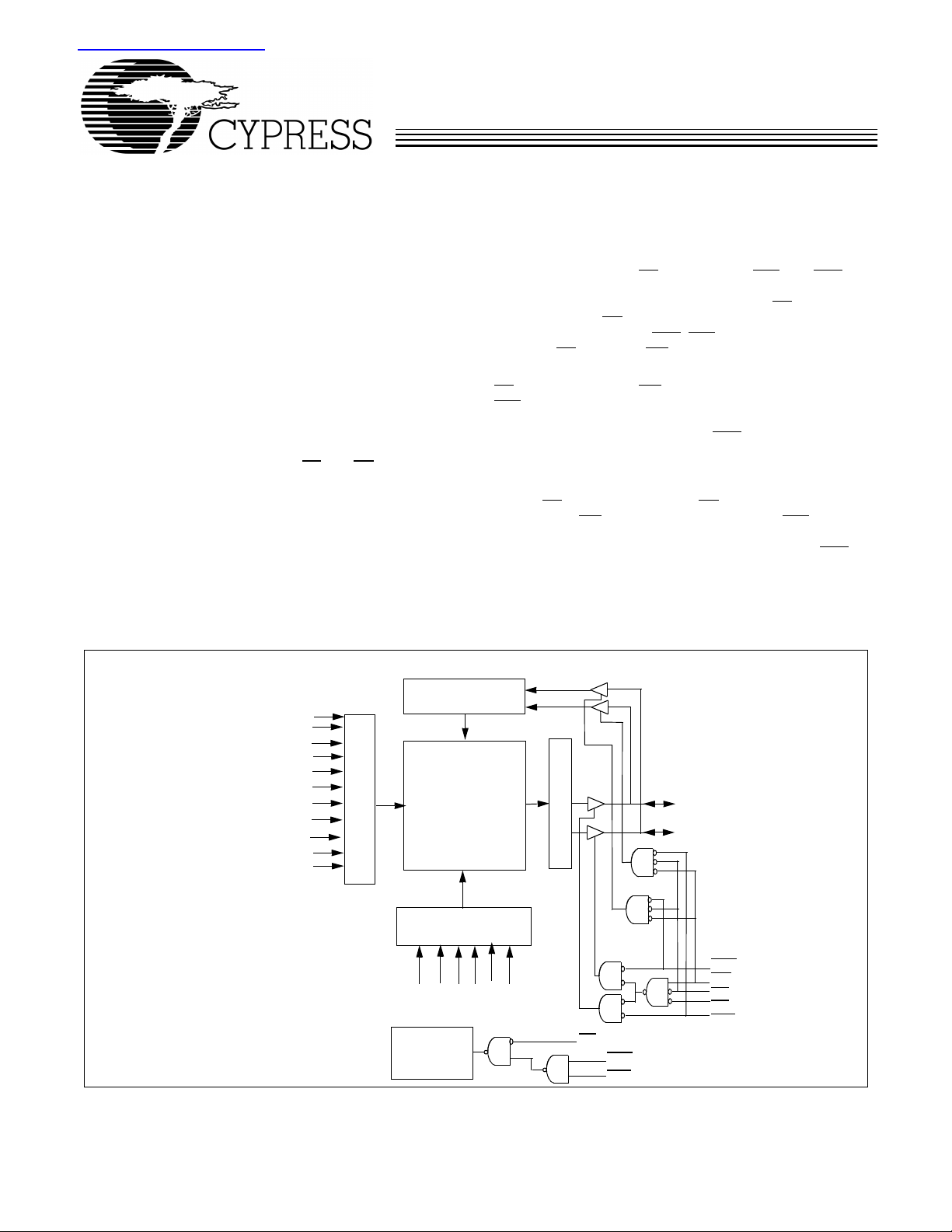
Logic Block Diagram
10
A
10
A
9
A
8
A
7
A
6
A
5
A
4
A
3
A
2
A
1
A
0
Note:
1. For best practice recommendations, please refer to the Cypress applic a tion note “System Design Guidelines” on http://www.cypress.com.
DATA IN DRIVERS
ROW DECODER
COLUMN DECODER
11
A
Power- down
Circuit
128K x 16
RAM Array
2048 x 1024
14
A12A13A
– I/O
I/O
0
7
SENSE AMPS
15
16
A
A
CE
BHE
BLE
I/O8 – I/O
BHE
WE
CE
OE
BLE
15
Cypress Semiconductor Corporation • 3901 North First Street • San Jose • CA 95134 • 408-943-2600
Document #: 38-05201 Rev. *D Revised September 20, 2002

CY62137CV25/30/33 MoBL
CY62137CV MoBL
®
®
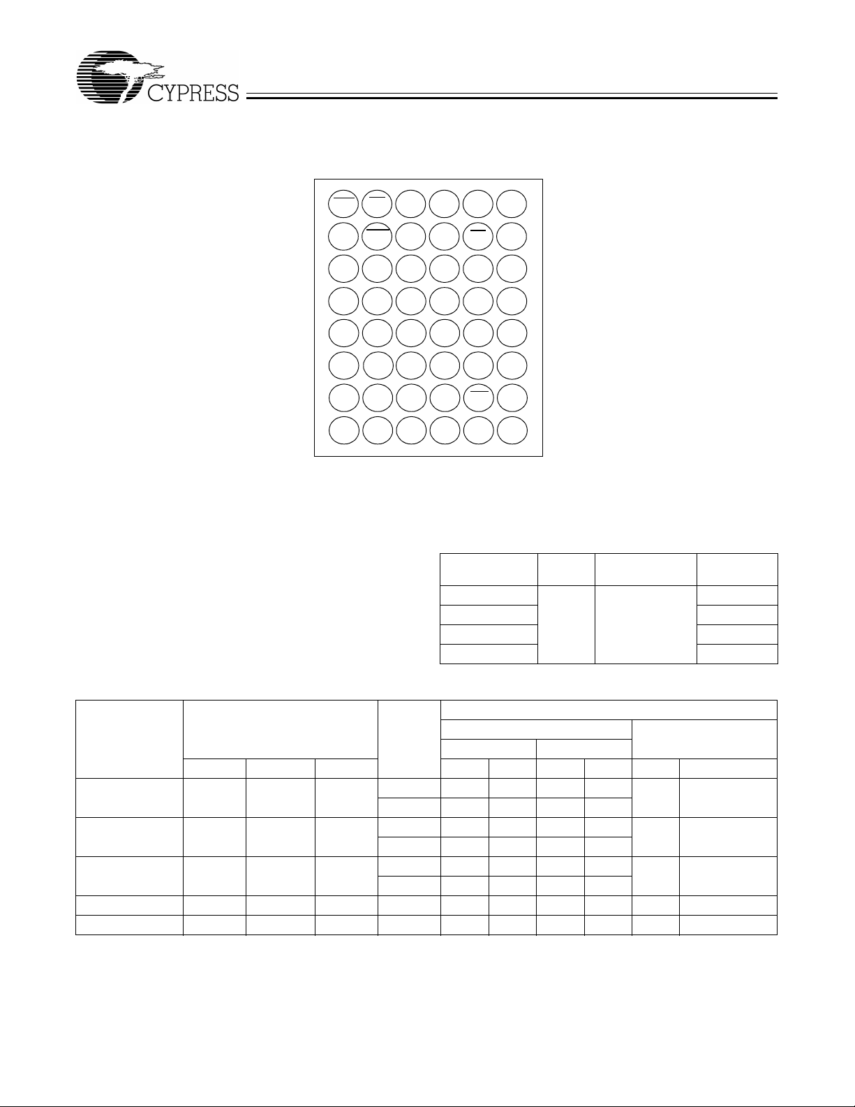
Pin Configuration
[2, 3]
FBGA (Top View)
4
5
6
A
A
1
A
4
A
6
A
7
A
16
A
15
A
13
A
10
CE
I/O
I/O
I/O
I/O
WE
A
NC
2
I/O
I/O
1
V
CC
3
V
SS
4
I/O
5
I/O
NC
11
A
B
0
C
2
D
E
F
6
G
7
H
A
A
A
NC
A
A
A
3
0
3
5
14
12
9
Static Discharge Voltage.......................................... > 2001V
Maximum Ratings
1
BLE
I/O
I/O
V
SS
V
CC
I/O
I/O
NC
2
OE
BHE
8
I/O
10
9
I/O
11
DNU
I/O
12
I/O
13
14
NC
15
A
8
(per MIL-STD-883, Method 3015)
(Above which the useful life may be impaired. For user guidelines, not tested.)
Storage Temperature .................................–65°C to +150°C
Ambient Temperature with
Power Applied.............................................–55°C to +125°C
Supply Voltage to Ground Potential –0.5V to V
DC Voltage Applied to Outputs
in High-Z State
DC Input Voltage
[4]
....................................–0.5V to VCC + 0.3V
[4]
....................................−0.5V to VCC + 0.3V
CCMAX
+ 0.5V
Latch-up Current................................................... > 200 mA
Operating Range
Device Range
CY62137CV25 Industrial –40°C to +85°C 2.2V to 2.7V
CY62137CV30 2.7V to 3.3V
CY62137CV33 3.0V to 3.6V
CY62137CV 2.7V to 3.6V
Ambient
Temperature T
A
Output Current into Outputs (LOW).............................20 mA
Product Portfolio
Power Dissipation
Operating, ICC (mA)
V
Range (V)
Product
CC
V
CC(min.)VCC(typ.)
[5]
V
CC(max.)
Speed
(ns)
Typ.
[5]
Max. Typ.
max
[5]
Max. Typ.
CY62137CV25LL 2.2 2.5 2.7 55 1.5 3 7 15 2 10
70 1.5 3 5.5 12
CY62137CV30LL 2.7 3.0 3.3 55 1.5 3 7 15 2 10
70 1.5 3 5.5 12
CY62137CV33LL 3.0 3.3 3.6 55 1.5 3 7 15 5 15
70 1.5 3 5.5 12
CY62137CVLL 2.7V 3.3 3.6 70 1.5 3 5.5 12 5 15
CY62137CVSL 2.7V 3.3 3.6 70 1.5 3 5.5 12 1 5
Standby, I
[5]
SB2
Max.
V
CC
(µA)f = 1 MHz f = f
Notes:
2. NC pins are not connected to the die.
3. E3 (DNU) can be left as NC or V
4. V
5. Typical values are included for reference only and are not guaranteed or tested. Typical values are measured at V
= –2.0V for pulse durations less than 20 ns.
IL(min.)
to ensure proper application.
SS
= V
CC
CC(typ.)
, TA = 25°C.
Document #: 38-05201 Rev. *D Page 2 of 13

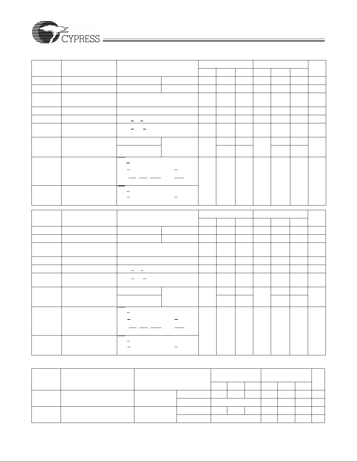
Electrical Characteristics Ov er the Op erat ing Range
Parameter Description Test Conditions
V
V
V
V
I
IX
I
OZ
I
CC
I
SB1
I
SB2
OH
OL
IH
IL
Output HIGH Voltage IOH = –0.1 mA VCC = 2.2V 2.0 2.0 V
Output LOW Voltage IOL = 0.1 mA VCC = 2.2V 0.4 0.4 V
Input HIGH Voltage 1.8 VCC +
Input LOW Voltage –0.3 0.6 –0.3 0.6 V
Input Leakage Current GND < VI < V
Output Leakage
GND < VO < VCC, Output Disabled –1 +1 –1 +1 µA
CC
Current
VCC Operating Supply
Current
Automatic CE
Power-down Current—
CMOS Inputs
Automatic CE
Power-down Current—
CMOS Inputs
f = f
f = 1 MHz 1.5 3 1.5 3
MAX
= 1/t
RC
VCC = 2.7V
I
OUT
CMOS Levels
CE > VCC – 0.2V
V
> VCC – 0.2V or VIN < 0.2V,
IN
f = f
(Address and Data Only),
max
f=0 (OE
, WE, BHE, and BLE)
CE > VCC – 0.2V
> VCC – 0.2V or VIN < 0.2V,
V
IN
f = 0, VCC = 2.7V
= 0 mA
CY62137CV25/30/33 MoBL
CY62137CV MoBL
CY62137CV25-55 CY62137CV25-70
[5]
Max. Min. Typ.
1.8 VCC +
0.3V
–1 +1 –1 +1 µA
7 15 5.5 12 mA
2 10 2 10 µA
[5]
Max.
UnitMin. Typ.
V
0.3V
®
®
Parameter Description Test Conditions
V
V
V
V
I
IX
I
OZ
I
CC
I
SB1
I
SB2
OH
OL
IH
IL
Output HIGH Voltage IOH = –1.0 mA VCC = 2.7V 2.4 2.4 V
Output LOW Voltage IOL = 2.1 mA VCC = 2.7V 0.4 0.4 V
Input HIGH Voltage 2.2 VCC +
Input LOW Voltage –0.3 0.8 –0.3 0.8 V
Input Leakage Current GND < VI < V
Output Leakage
GND < VO < VCC, Output Disabled –1 +1 –1 +1 µA
CC
Current
VCC Operating Supply
Current
Automatic CE
Power-down Current—
CMOS Inputs
Automatic CE
Power-down Current—
CMOS Inputs
f = f
f = 1 MHz 1.5 3 1.5 3
MAX
= 1/t
RC
VCC = 3.3V
= 0 mA
I
OUT
CMOS Levels
CE > VCC – 0.2V
V
> VCC – 0.2V or VIN < 0.2V,
IN
f = f
(Address and Data Only),
max
f=0 (OE
, WE, BHE, and BLE)
CE > VCC – 0.2V
VIN > VCC – 0.2V or VIN < 0.2V,
CC
= 3.3V
f = 0, V
Electrical Characteristics Ov er the Op erat ing Range
Parameter Description Test Conditions
V
OH
V
OL
Output HIGH Voltage IOH = –1.0 mA VCC = 3.0V 2.4 2.4 V
VCC = 2.7V 2.4 V
Output LOW Voltage IOL = 2.1 mA VCC = 3.0V 0.4 0.4 V
VCC = 2.7V 0.4 V
CY62137CV30-55 CY62137CV30-70
[5]
Max. Min. Typ.
2.2 VCC +
0.3V
[5]
Max.
UnitMin. Typ.
V
0.3V
–1 +1 –1 +1 µA
7 15 5.5 12 mA
2 10 2 10 µA
CY62137CV33-70
CY62137CV33-55
[5]
Max. Min. Typ.
CY62137CV-70
[5]
Max.
UnitMin. Typ.
Document #: 38-05201 Rev. *D Page 3 of 13

Electrical Characteristics Ov er the Op erat ing Range (continued)
Parameter Description Test Conditions
V
IH
V
IL
I
IX
I
OZ
I
CC
I
SB1
I
SB2
Capacitance
C
IN
C
OUT
Input HIGH Voltage 2.2 VCC +
Input LOW Voltage –0.3 0.8 –0.3 0.8 V
Input Leakage Current GND < VI < V
CC
Output Leakage Current GND < VO < VCC, Output Dis-
abled
VCC Operating Supply Current f = f
f = 1 MHz 1.5 3 1.5 3
MAX
= 1/t
RCVCC
I
OUT
CMOS
= 3.6V
= 0 mA
Levels
Automatic CE
Power-down Current —CMOS
Inputs
Automatic CE
Power-down Current —CMOS
Inputs
[6]
CE > VCC – 0.2V
V
> VCC – 0.2V or VIN < 0.2V,
IN
f = f
(Address and Data Onl y),
max
f=0 (OE
, WE, BHE, and BLE)
CE > VCC – 0.2V
VIN > VCC – 0.2V or VIN <
0.2V,
CC
= 3.6V
f = 0, V
Parameter Description Test Conditions Max. Unit
Input Capacitance TA = 25°C, f = 1 MHz,
= V
V
CC
Output Capacitance 8 pF
CC(typ.)
CY62137CV25/30/33 MoBL
CY62137CV MoBL
CY62137CV33-55
[5]
Max. Min. Typ.
0.3V
–1 +1 –1 +1 µA
–1 +1 –1 +1 µA
7 15 5.5 12 mA
5 15 5 15 µA
LL 5 15 5 15
SL 1 5
CY62137CV33-70
CY62137CV-70
[5]
Max.
2.2 VCC +
0.3V
6 pF
®
®
UnitMin. Typ.
V
Thermal Resistance
Parameter Description T est Condit ions BGA Unit
Θ
Θ
Thermal Resistance
JA
(Junction to Ambient)
Thermal Resistance
JC
(Junction to Case)
[6]
[6]
Still Air, soldered on a 3 x 4.5 inch, two-layer printed
circuit board
55 °C/W
16 °C/W
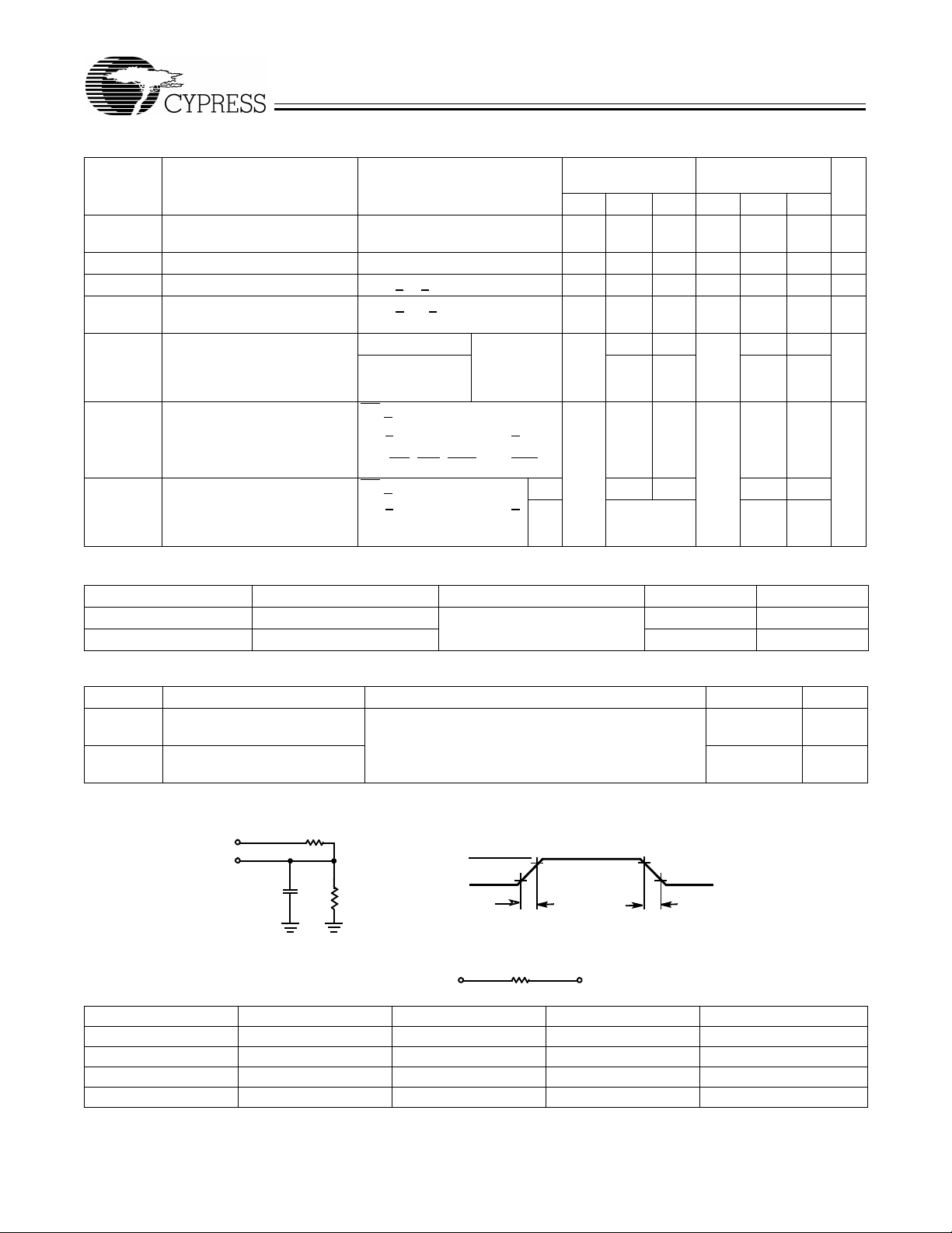
AC Test Loads and Waveforms
30 pF
SCOPE
R1
VCC Typ
R2
Equivalent to: THÉ VENIN EQUIVALENT
GND
Rise TIme: 1 V/ns Fall Time: 1 V/ns
OUTPUT V
10%
ALL INPUT PULSES
90%
R
TH
TH
90%
10%
8000 645 645 Ω
1.20 1.75 1.75 V
V
CC
OUTPUT
INCLUDING
JIG AND
Parameters 2.5V 3.0V 3.3V Unit
R1 16600 1105 1216 Ω
R2 15400 1550 1374 Ω
R
TH
V
Note:
6. Tested initially and after any design or process changes that may affect these parameters.
TH
Document #: 38-05201 Rev. *D Page 4 of 13
 Loading...