

Page 1
CY62136EV30
MoBL
®
2-Mbit (128K x 16) Static RAM
Features
• Very high speed: 45 ns
• Wide voltage range: 2.20V–3.60V
• Pin-compatible with CY62136CV30
• Ultra low standby power
— Typical standby current: 1µA
— Maximum standby current: 7µA
• Ultra-low active power
— Typical active current: 2 mA @ f = 1 MHz
• Easy memory expansion with CE
• Automatic power-down when deselected
• CMOS for optimum speed/power
• Offered in a Pb-free 48-ball VFBGA and 44-pin TSOP II
packages
, and OE features
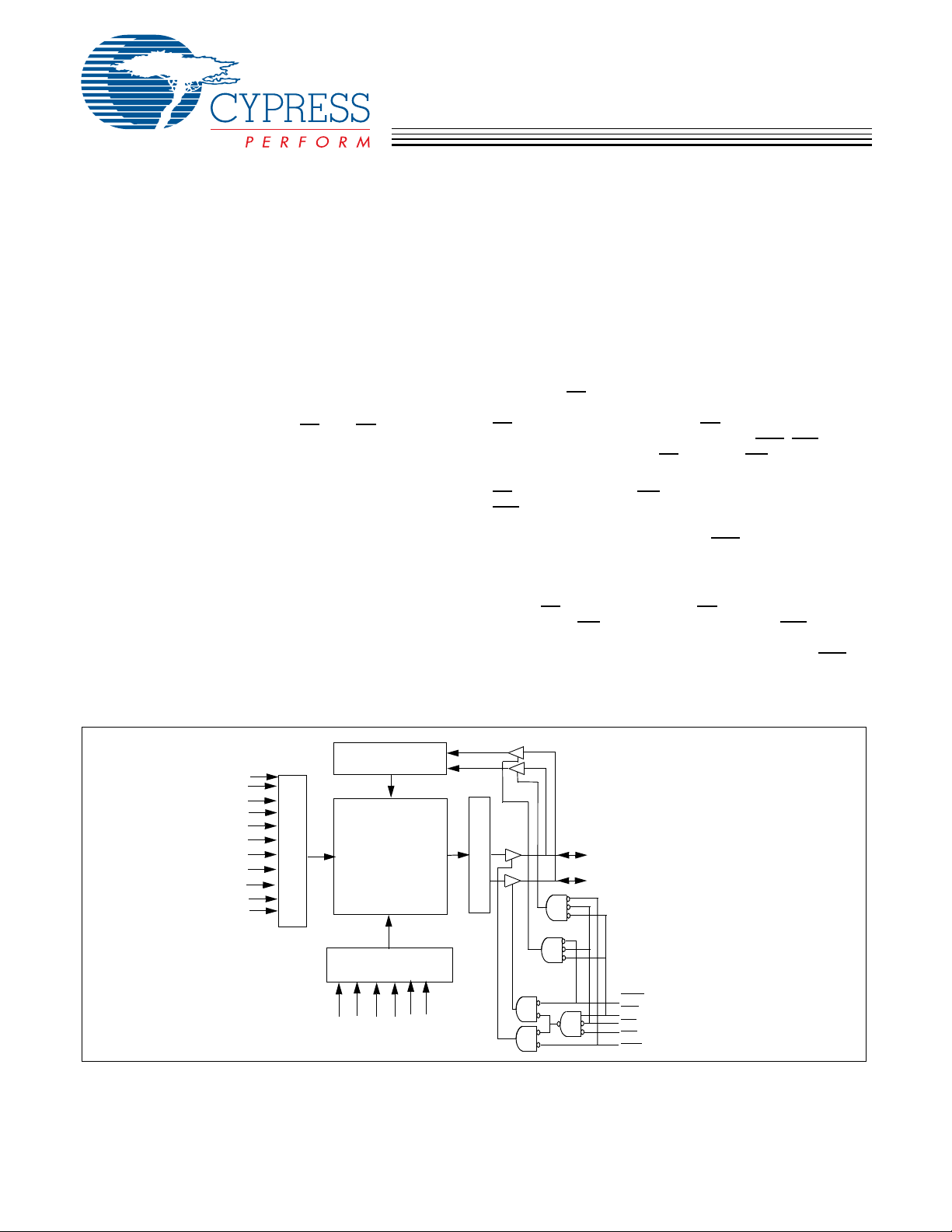
Functional Description
[1]
The CY62136EV30 is a high-performance CMOS static RAM
organized as 128K words by 16 bits. This device features
advanced circuit design to provide ultra-low active current.
This is ideal for providing More Battery Life™ (MoBL
®
) in
portable applications such as cellular telephones. The device
also has an automatic power-down feature that significantly
reduces power consumption by 80% when addresses are not
toggling. The device can also be put into standby mode
reducing power consumption by more than 99% when
deselected (CE
) are placed in a high-impedance state when: deselected
I/O
15
(CE
HIGH), outputs are disabled (OE HIGH), both Byte High
Enable and Byte Low Enable are disabled (BHE
or during a write operation (CE
HIGH). The input/output pins (I/O0 through
, BLE HIGH),
LOW and WE LOW).
Writing to the device is accomplished by taking Chip Enable
) and Write Enable (WE) inputs LOW. If Byte Low Enable
(CE
(BLE
) is LOW, then data from I/O pins (I/O0 through I/O7), is
written into the location specified on the address pins (A
through A16). If Byte High Enable (BHE) is LOW, then data
from I/O pins (I/O
specified on the address pins (A
through I/O15) is written into the location
8
through A16).
0
Reading from the device is accomplished by taking Chip
Enable (CE
Write Enable (WE
) and Output Enable (OE) LOW while forcing the
) HIGH. If Byte Low Enable (BLE) is LOW,
then data from the memory location specified by the address
pins will appear on I/O
LOW, then data from memory will appear on I/O
the truth table at the back of this data sheet for a complete
to I/O7. If Byte High Enable (BHE) is
0
to I/O15. See
8
description of read and write modes.
0
Logic Block Diagram
A
10
A
9
A
8
A
7
A
6
A
5
A
4
A
3
A
2
A
1
A
0
Note:
1. For best practice recommendations, please refer to the Cypress application note “System Design Guidelines” on http://www.cypress.com.
Cypress Semiconductor Corporation • 198 Champion Court • San Jose, CA 95134-1709 • 408-943-2600
Document #: 38-05569 Rev. *B Revised January 6, 2006
DATA IN DRIVERS
ROW DECODER
COLUMN DECODER
11
A
128K x 16
RAM Array
13
A12A
–I/O
I/O
0
7
SENSE AMPS
16
15
14
A
A
A
I/O8–I/O
15
BHE
WE
CE
OE
BLE
[+] Feedback
Page 2
CY62136EV30
MoBL
®
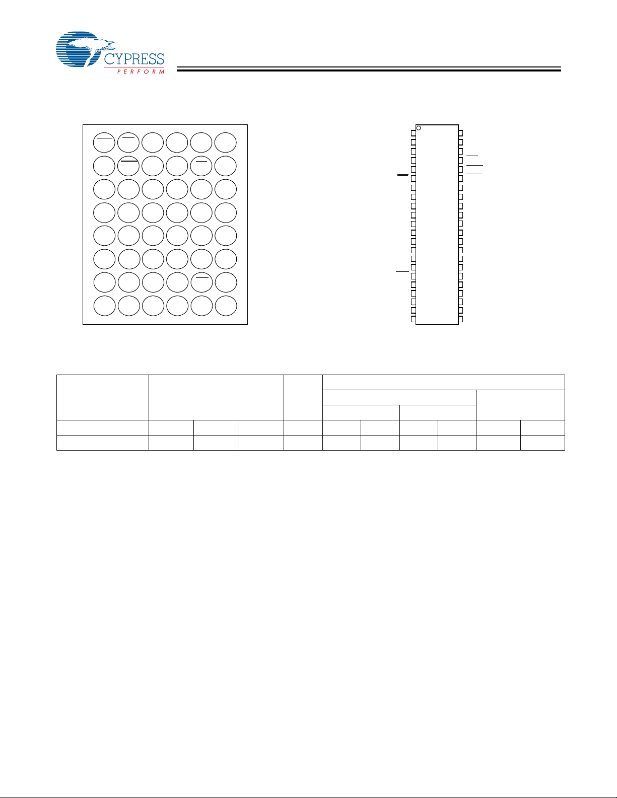
Pin Configuration
1
2
OE
BLE
I/O
BHE
8
I/O
I/O
V
V
I/O
I/O
NC
SS
CC
10
9
I/O
11
I/O
12
I/O
13
14
NC
15
A
8
Product Portfolio
[2, 3]
VFBGA (Top View) 44 TSOP II (Top View)
4
3
A
A
A
NC
NC
A
14
A
12
A
[4]
0
3
5
9
5
6
A
A
1
A
4
A
6
A
7
A
16
A
15
A
13
A
10
CE
I/O
I/O
I/O
I/O
WE
A
NC
2
I/O
I/O
1
Vcc
3
Vss
4
I/O
5
I/O
NC
11
A
B
0
C
2
D
E
F
6
G
7
H
CE
I/O
I/O
I/O
I/O
V
V
I/O
I/O
I/O
I/O
WE
A
A
A
A
A
A
A
A
A
A
CC
SS
44
1
4
2
3
3
2
4
1
5
0
6
7
0
8
1
9
2
10
3
11
12
13
4
14
5
15
6
16
7
17
18
16
19
15
20
14
21
13
22
12
A
5
43
A
6
42
A
7
41
OE
40
BHE
39
BLE
38
I/O
37
I/O
36
I/O
35
I/O
34
V
SS
33
V
CC
32
I/O
31
I/O
30
I/O
29
I/O
NC
28
27
A
8
26
A
9
25
A
10
A
24
11
23
NC
15
14
13
12
11
10
9
8
Power Dissipation
Operating ICC (mA)
[4]
Max. Typ.
max
[4]
Max. Typ.
Standby I
[4]
SB2
Max.
Product VCC Range (V)
Min. Typ.
[4]
Speed
(ns)
Max. Typ.
CY62136EV30LL 2.2 3.0 3.6 45 2 2.5 15 20 1 7
Notes:
2. NC pins are not connected on the die.
3. Pins D3, H1, G2, and H6 in the BGA package are address expansion pins for 4 Mbit, 8 Mbit, 16 Mbit and 32 Mbit, respectively.
4. Typical values are included for reference only and are not guaranteed or tested. Typical values are measured at V
CC
= V
CC(typ.)
, TA = 25°C.
(µA)f = 1MHz f = f
Document #: 38-05569 Rev. *B Page 2 of 12
[+] Feedback
Page 3
CY62136EV30
MoBL
®
Maximum Ratings
(Above which the useful life may be impaired. For user guidelines, not tested.)
Storage Temperature ................................–65°C to + 150°C
Ambient Temperature with
Power Applied ...........................................–55°C to + 125°C
Supply Voltage to Ground
Potential ..............................–0.3V to 3.9V (V
DC Voltage Applied to Outputs
in High-Z State
[5,6]
................–0.3V to 3.9V (V
Electrical Characteristics Over the Operating Range
Parameter Description Test Conditions
V
V
V
V
I
IX
I
OZ
I
CC
I
SB1
OH
OL
IH
IL
Output HIGH
Voltage
Output LOW
Voltage
Input HIGH Volt age V
Input LOW Voltage V
Input Leakage
Current
Output Leakage
Current
VCC Operating
Supply Current
Automatic CE
Power-down
Current — CMOS
Inputs
I
SB2
Automatic CE
Power-down
Current — CMOS
Inputs
Capacitance (for all packages)
IOH = –0.1 mA V
= –1.0 mA V
I
OH
IOL = 0.1 mA V
= 2.1mA V
I
OL
= 2.2V to 2.7V 1.8 V
CC
= 2.7V to 3.6V 2.2 V
V
CC
= 2.2V to 2.7V –0.3 0.6 V
CC
= 2.7V to 3.6V –0.3 0.8 V
V
CC
GND < VI < V
GND < VO < VCC, Output Disabled –1 +1 µA
f = f
= 1/tRCVCC = V
MAX
f = 1 MHz 2 2.5
CE > VCC−0.2V ,
V
f = f
f = 0 (OE
V
–0.2V, VIN<0.2V)
IN>VCC
(Address and Data Only),
MAX
, and WE),
= 3.60V
CC
CE > VCC – 0.2V,
V
> VCC – 0.2V or VIN < 0.2V, f = 0,
IN
V
= 3.60V
CC
[8]
CC MAX
CC MAX
CC
+ 0.3V)
+ 0.3V)
[5, 6, 7]
= 2.20V 2.0 V
CC
= 2.70V 2.4 V
CC
= 2.20V 0.4 V
CC
= 2.70V 0.4 V
CC
CMOS levels
CCmax, IOUT
DC Input Voltage
[5,6]
............ –0.3V to 3.9V (V
CC MAX
+ 0.3V)
Output Current into Outputs (LOW) ............................20 mA
Static Discharge Voltage ......................................... > 2001V
(per MIL-STD-883, Method 3015)
Latch-up Current ....................................................> 200 mA
Operating Range
Device Range
[7]
Ambient
T emperature V
CC
[7]
CY62136EV30LL Industrial –40°C to +85°C 2.2V - 3.6V
45 ns
[4]
Max.
+ 0.3 V
CC
+ 0.3 V
CC
UnitMin. Typ.
–1 +1 µA
= 0 mA
15 20 mA
17µA
17µA
Parameter Description Test Conditions Max. Unit
C
IN
C
OUT
Notes:
5. V
6. V
7. Full Device AC operation assumes a 100 µs ramp time from 0 to Vcc(min) and 200 µs wait time after V
8. Tested initially and after any design or process ch anges that may affect these parameters.
= –2.0V for pulse durations less than 20 ns.
IL(min.)
IH(max)=VCC
+0.75V for pulse durations less than 20ns.
Input Capacitance TA = 25°C, f = 1 MHz,
V
= V
CC
Output Capacitance 10 pF
CC(typ)
stabilization.
CC
10 pF
Document #: 38-05569 Rev. *B Page 3 of 12
[+] Feedback
Page 4
CY62136EV30
MoBL
®
Thermal Resistance
[8]
VFBGA
Parameter Description Test Conditions
Θ
Θ
Thermal Resistance
JA
(Junction to Ambient)
Thermal Resistance
JC
(Junction to Case)
[8]
[8]
Still Air, soldered on a 3 × 4.5 inch, two-layer
printed circuit board
Package
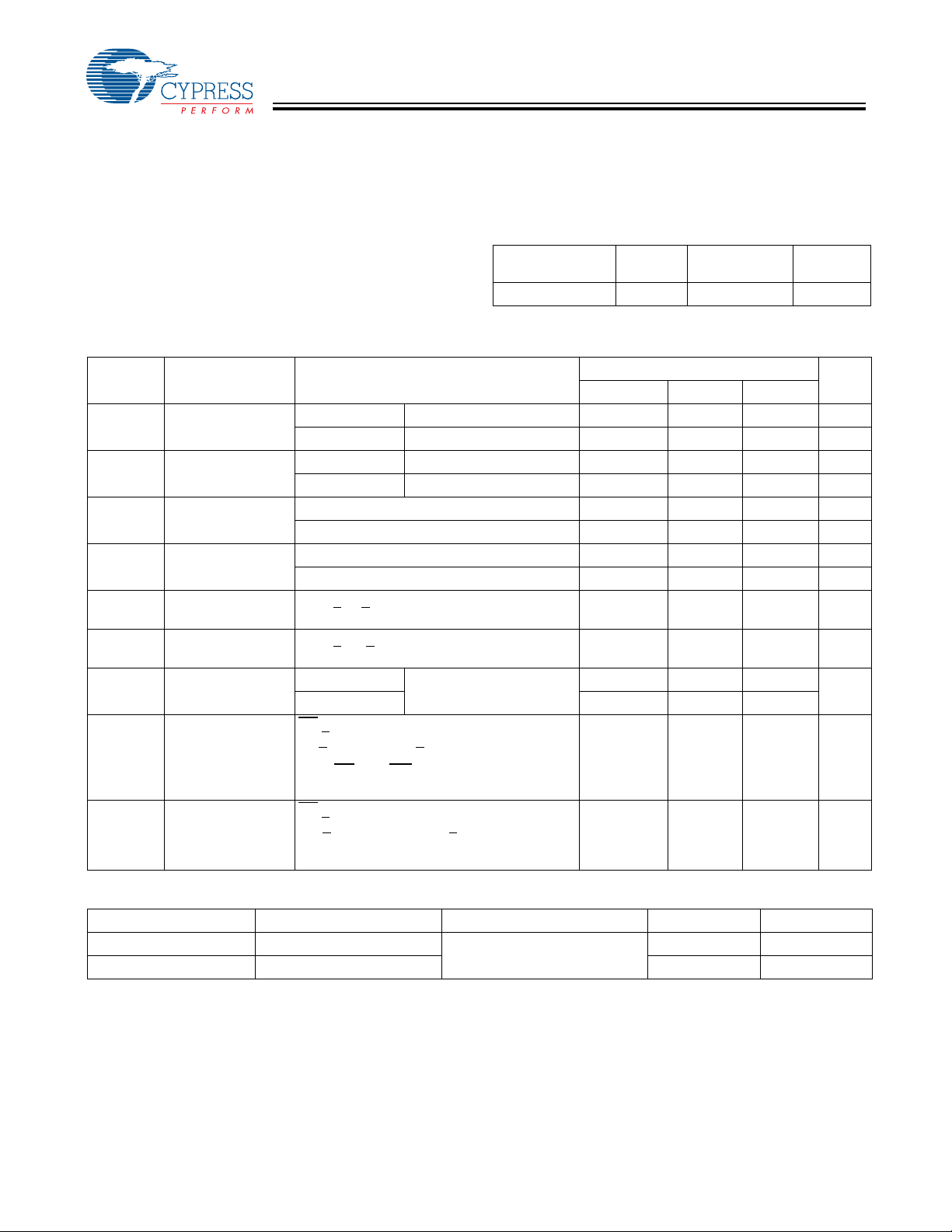
AC Test Loads and Waveforms
R1
V
CC
OUTPUT
INCLUDING
JIG AND
30 pF
R2
VCC
GND
Rise Time = 1 V/ns
Equivalent to: THÉVENIN EQUIVALENT
10%
SCOPE
Parameters 2.50V 3.0V Unit
R1 16667 1103 Ω
R2 15385 1554 Ω
R
TH
V
TH
8000 645 Ω
1.20 1.75 V
Data Retention Characteristics (Over the Operating Range)
Parameter Description Conditions Min. Typ.
V
DR
I
CCDR
[8]
t
CDR
[9]
t
R
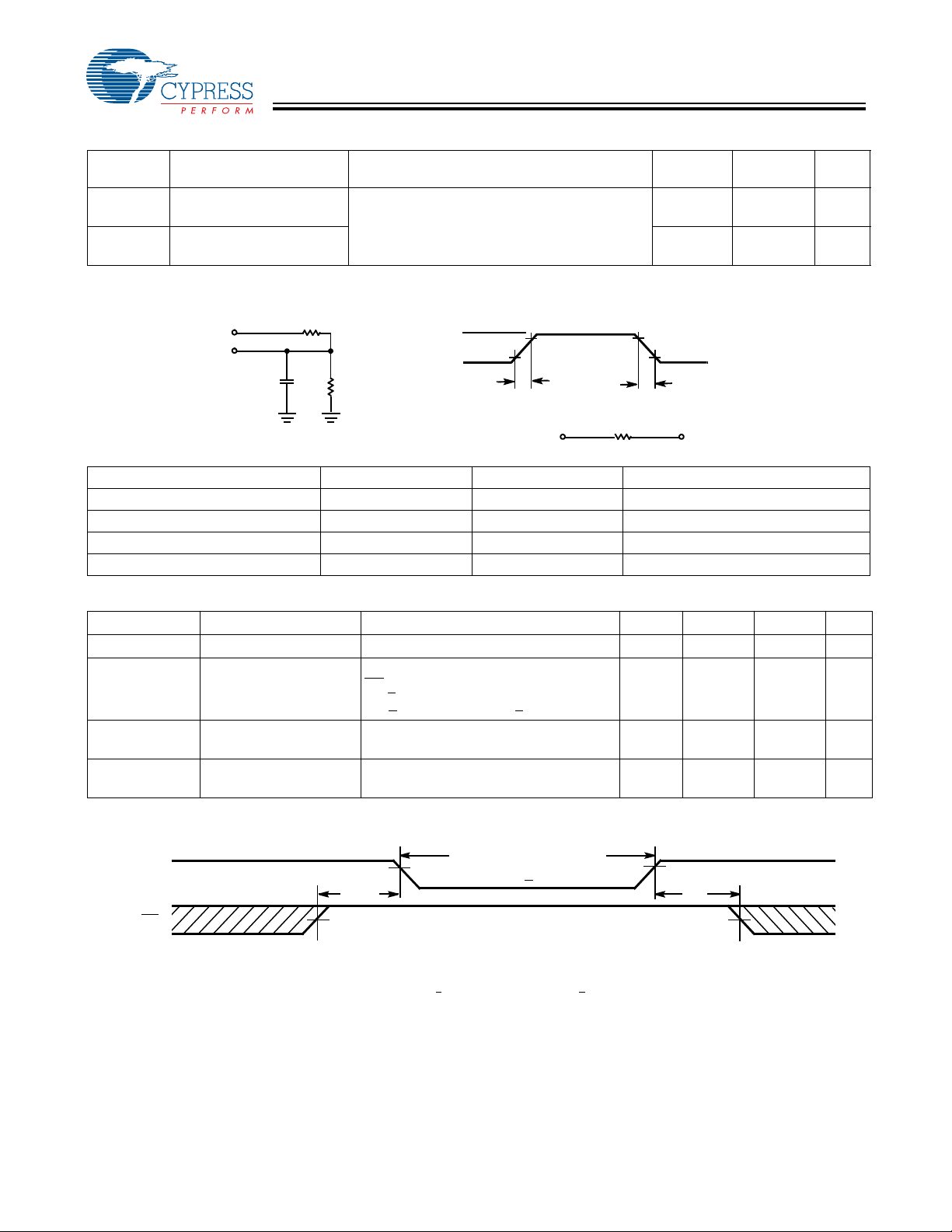
Data Retention Waveform
V
CC
CE
VCC for Data Retention 1.0 V
Data Retention Current VCC= 1.0V
CE
> VCC – 0.2V,
V
> VCC – 0.2V or VIN < 0.2V
IN
Chip Deselect to Data
Retention Time
Operation Recovery
Time
V
CC(min)
t
CDR
DATA RETENTION MODE
ALL INPUT PULSES
90%
OUTPUT V
[8, 9]
90%
10%
R
TH
0ns
t
RC
VDR> 1.0 V
V
TSOP II
Package Unit
75 77 °C/W
10 13 °C/W
Fall Time = 1 V/ns
TH
[4]
Max. Unit
0.8 3 µA
CC(min)
t
R
ns
Notes:
9. Full device operation requires linear V
ramp from V
CC
DR
to V
> 100 µs or stab le at V
CC(min.)
CC(min.)
> 100 µs.
Document #: 38-05569 Rev. *B Page 4 of 12
[+] Feedback
Page 5

CY62136EV30
MoBL
®
Switching Characteristics Over the Operating Range
[10, 11, 12, 13]
45 ns
Parameter Description
Read Cycle
t
RC
t
AA
t
OHA
t
ACE
t
DOE
t
LZOE
t
HZOE
t
LZCE
t
HZCE
t
PU
t
PD
t
DBE
t
LZBE
t
HZBE
Write Cycle
t
WC
t
SCE
t
AW
t
HA
t
SA
t
PWE
t
BW
t
SD
t
HD
t
HZWE
t
LZWE
Notes:
10.Test conditions for all p arameters other t han tri-st ate para meters assume signal tran sition ti me of 3 ns (1V/ns) o r less, ti ming reference l evels of V
pulse levels of 0 to V
11.At any given temperature and voltage condition, t
given device.
12.t
HZOE
13.The internal Write time of the memory is defined by the overlap of WE
of these signals can terminate a write by going INACTIVE. The data i nput set-up an d hol d ti mi ng should be r efe renced to the edge o f the sign al t hat te rminat es
the write.
, t
HZCE
[13]
, t
HZBE
CC(typ.)
, and t
Read Cycle Time 45 ns
Address to Data Valid 45 ns
Data Hold from Address Change 10 ns
CE LOW to Data Valid 45 ns
OE LOW to Data Valid 22 ns
OE LOW to LOW Z
OE HIGH to High Z
CE LOW to Low Z
CE HIGH to High Z
[11]
[11, 12]
[11]
[11, 12]
5ns
18 ns
10 ns
18 ns
CE LOW to Power-Up 0 ns
CE HIGH to Power-Down 45 ns
BLE/BHE LOW to Data Valid 22 ns
BLE/BHE LOW to Low Z
BLE/BHE HIGH to HIGH Z
[11]
[11, 12]
5ns
18 ns
Write Cycle Time 45 ns
CE LOW to Write End 35 ns
Address Set-Up to Write End 35 ns
Address Hold from Write End 0 ns
Address Set-Up to Write Start 0 ns
WE Pulse Width 35 ns
BLE/BHE LOW to Write End 35 ns
Data Set-Up to Write End 25 ns
Data Hold from Write End 0 ns
is less than t
HZCE
[11, 12]
[11]
18 ns
10 ns
, t
LZCE
is less than t
HZBE
, CE = VIL, BHE and/or BLE = VIL. All signals must be ACTIVE to initiate a write and any
LZBE
, t
HZOE
is less than t
LZOE
, and t
HZWE
is less than t
WE LOW to High-Z
WE HIGH to Low-Z
, and output loading of the specified IOL/IOH as shown in the “AC Test Loads and Waveforms” section.
transitions are measured when the outputs enter a high impedence state.
HZWE
CC(typ)
LZWE
UnitMin. Max.
/2, input
for any
Document #: 38-05569 Rev. *B Page 5 of 12
[+] Feedback
Page 6

CY62136EV30
MoBL
®
Switching Waveforms
Read Cycle 1 (Address Transition Controlled)
[14, 15]
[14, 15]
t
RC
ADDRESS
t
t
OHA
AA
DATA OUT PREVIOUS DATA VALID DATA VALID
Read Cycle No. 2 (OE Controlled)
ADDRESS
CE
[15, 16]
t
ACE
t
RC
OE
t
DOE
BHE/BLE
t
LZOE
t
HZCE
t
HZOE
t
PD
t
DBE
t
LZBE
DATA OUT
V
CC
SUPPLY
CURRENT
Notes:
The device is continuously selected. OE, C E = VIL, BHE and/or BLE = VIL.
14.
is HIGH for read cycle.
15.WE
16.Address valid prior to or coincident with CE
HIGH IMPEDANCE
t
LZCE
t
PU
and BHE, BLE transition LOW.
50%
DATA VALID
t
HZBE
50%
HIGH
IMPEDANCE
I
CC
I
SB
Document #: 38-05569 Rev. *B Page 6 of 12
[+] Feedback
Page 7

CY62136EV30
MoBL
®
Switching Waveforms (continued)
19
[13, 17, 18]
t
SA
t
HZOE
[13, 17, 18]
Write Cycle No. 1 (WE Controlled)
ADDRESS
CE
WE
BHE/BLE
OE
DATA I/O
NOTE
Write Cycle No. 2 (CE Controlled)
[14, 15]
t
WC
t
SCE
t
AW
t
PWE
t
BW
t
SD
DATA
IN
t
HA
t
HD
t
WC
ADDRESS
CE
t
SA
t
AW
WE
t
BHE/BLE
BW
OE
DATA I/O
Notes:
17.Data I/O is high impedance if OE
18.If CE
goes HIGH simultaneously with WE = VIH, the output remains in a high-impedance state.
19.During this period, the I/Os are in output state and input signals should not be applied.
NOTE
19
= VIH.
t
HZOE
t
PWE
t
SD
DATA
t
SCE
IN
t
HA
t
HD
Document #: 38-05569 Rev. *B Page 7 of 12
[+] Feedback
Page 8

CY62136EV30
MoBL
®
Switching Waveforms (continued)
Write Cycle No. 3 (WE Controlled, OE LOW)
[14, 15]
[18]
ADDRESS
CE
BHE/BLE
t
SA
WE
DATAI/O
NOTE 19
t
HZWE
Write Cycle No. 4 (BHE/BLE Controlled, OE LOW)
[18]
t
AW
t
t
SCE
BW
t
t
WC
WC
t
PWE
t
SD
DATAIN
t
HA
t
HD
t
LZWE
ADDRESS
CE
BHE/BLE
WE
DATA I/O
t
SA
NOTE 19
t
HZWE
t
SCE
t
AW
t
BW
t
PWE
t
SD
DATA
IN
t
HA
t
HD
t
LZWE
Document #: 38-05569 Rev. *B Page 8 of 12
[+] Feedback
Page 9

CY62136EV30
Truth Table
CE WE OE BHE BLE Inputs/Outputs Mode Power
H X X X X High Z Deselect/Power-down S tandby (ISB)
L X X H H High Z Output Disabled Active (I
L H L L L Data Out (I/O
L H L H L Data Out (I/O
I/O
–I/O
8
L H L L H Data Out (I/O8–I/O15);
–I/O7 in High Z
I/O
0
–I/O15) Read Active (ICC)
O
in High Z
15
–I/O7);
O
Read Active (I
Read Active (I
L H H L L High Z Output Disabled Active (I
L H H H L High Z Output Disabled Active (I
L H H L H High Z Output Disabled Active (I
L L X L L Data In (I/O
L L X H L Data In (I/O
I/O
–I/O
8
L L X L H Data In (I/O
I/O
–I/O7 in High Z
0
–I/O15) Write Active (ICC)
O
O
in High Z
15
–I/O15);
8
–I/O7);
Write Active (I
Write Active (I
Ordering Information
Speed
(ns) Ordering Code
45 CY62136EV30LL-45BVXI 51-85150 48-ball Very Fine Pitch Ball Grid Array (Pb-free) Industrial
CY62136EV30LL-45ZSXI 51-85087 44-pin Thin Small Outline Package II (Pb-free)
Please contact your local Cypress sales representative for availability of other parts
Package
Diagram Package Type
MoBL
)
CC
)
CC
)
CC
)
CC
)
CC
)
CC
)
CC
)
CC
Operating
Range
®
Document #: 38-05569 Rev. *B Page 9 of 12
[+] Feedback
Page 10

Package Diagrams
48-pin VFBGA (6 x 8 x 1 mm) (51-85150)
CY62136EV30
MoBL
®
0.25 C
8.00±0.10
A
0.55 MAX.
TOP VIEW
A1 CORNER
465231
A
B
C
D
E
F
G
H
A
B
6.00±0.10
0.21±0.05
0.10 C
0.75
5.25
8.00±0.10
2.625
B
0.15(4X)
BOTTOM VIEW
Ø0.05 M C
Ø0.25 M C A B
Ø0.30±0.05(48X)
65
1.875
0.75
6.00±0.10
3.75
A1 CORNER
1
234
A
B
C
D
E
F
G
H
51-85150-*D
SEATING PLANE
C
0.26 MAX.
1.00 MAX
Document #: 38-05569 Rev. *B Page 10 of 12
[+] Feedback
Page 11

Package Diagrams (continued)
44-pin TSOP II (51-85087)
CY62136EV30
MoBL
®
51-85087-*A
MoBL is a registered trademark, and More Battery Life is a trademark, of Cypress Semicond uctor. All product and company
names mentioned in this document may be the trademarks of their respective holders.
Document #: 38-05569 Rev. *B Pa ge 11 of 12
© Cypress Semiconductor Corporation, 2006. The information contained herein is subject to ch ange without notice. Cypress Semiconductor Corporation assumes no resp onsib ility for the u se
of any circuitry other than circuitry embodied in a Cypress product. Nor does it convey or imply any license under patent or other rights. Cypress products are not warranted nor intended to be
used for medical, life support, life saving, critical control or safety applications, unless pursuant to an express written agreement with Cypress. Furtherm ore, Cypress do es not authori ze its
products for use as critical components in life-support systems where a malfunction or failure may reasonably be expected to result in significant injury to the user. The inclusion of Cypress
products in life-support systems application implies that the manufacturer assumes all risk of such use and in doing so indemnifies Cypress against all charges.
[+] Feedback
Page 12

Document History Page
Document Title: CY62136EV30 MoBL® 2-Mbit (128K x 16) Static RAM
Document Number: 38-05569
REV. ECN NO. Issue Date
** 237432 See ECN AJU New Data Sheet
*A 419988 See ECN RXU Converted from Advanced Information to Final.
*B 427817 See ECN NXR Minor change: Moved datasheet to external web
Orig. of
Change Description of Change
Changed the address of Cypress Semiconductor Corporation on Page #1
from “3901 North First Street” to “198 Champion Court”
Removed 35ns Speed Bin
Removed “L” version of CY62136EV30
Changed I
1.5 mA to 2 mA at f=1 MHz
(Max) value from 2 mA to 2.5 mA and ICC (Typ) value from
CC
Changed ICC (Typ) value from 12 mA to 15 mA at f = f
Changed I
2.5 µA to 7 µA.
SB1
and I
Typ. values from 0.7 µA to 1 µA and Max. values from
SB2
Changed the AC test load capacitance from 50pF to 30pF on Page# 4
Changed V
Changed I
Added I
Changed t
Changed t
Changed t
Changed t
Changed t
Changed t
Changed t
Corrected typo in the Truth Table on Page# 9
from 1.5V to 1V on Page# 4.
DR
from 2.5 µA to 3 µA.
CCDR
typical value.
CCDR
OHA , tLZCE
LZBE
LZOE
HZOE, tHZCE, tHZBE
SCE,tAW and tBW
PWE
from 20 ns to 25 ns
SD
and t
from 6 ns to 5 ns
from 3 ns to 5 ns
from 30 ns to 35 ns
Updated the package diagram 48-pin VFBGA from *B to *D
Updated the ordering Information table and replaced the Package Name
column with Package Diagram.
from 6 ns to 10 ns
LZWE
and t
from 40 ns to 35 ns
HZWE
CY62136EV30
max
from 15 ns to 18 ns
MoBL
®
Document #: 38-05569 Rev. *B Page 12 of 12
[+] Feedback
 Loading...